

查询M68AF127B供应商
FEAT URES SUM MARY
■ SUPPLY VOLTAGE: 4.5 to 5.5V
■ 128K x 8 bits SRAM with OUTPUT ENABLE
■ EQUAL CYCLE and ACCESS TIMES: 55ns
■ LOW STANDBY CURRENT
■ LOW V
■ TRI-STATE COMMON I/O
■ LOW ACTIVE and STANDBY POWE R
DATA RETENTION: 2V
CC
M68AF127B
1Mbit (128K x8), 5V Asynchronous SRAM
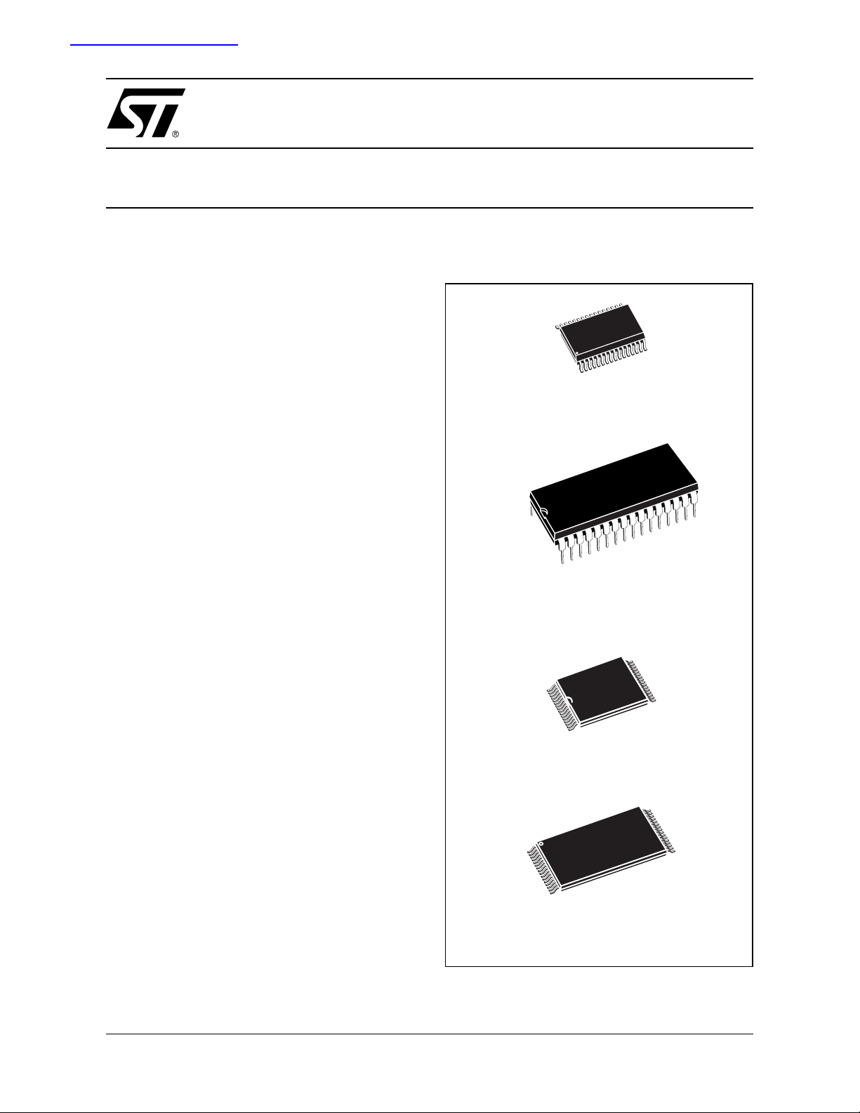
Figure 1. Packages
SO32 (MC)
32
1
PDIP32 (B)
TSOP32 (NK)
8 x 13.4mm
TSOP32 (N)
8 x 20mm
1/23September 2004

M68AF127B
TABLE OF CONTENTS
FEATURES SUMMARY . . . . . . . . . . . . . . . . . . . . . . . . . . . . . . . . . . . . . . . . . . . . . . . . . . . . . . . . . . . . . 1
Figure 1. Packages. . . . . . . . . . . . . . . . . . . . . . . . . . . . . . . . . . . . . . . . . . . . . . . . . . . . . . . . . . . . . . 1
TABLE OF CONTENTS . . . . . . . . . . . . . . . . . . . . . . . . . . . . . . . . . . . . . . . . . . . . . . . . . . . . . . . . . . . . . 2
SUMMARY DESCRIPTION. . . . . . . . . . . . . . . . . . . . . . . . . . . . . . . . . . . . . . . . . . . . . . . . . . . . . . . . . . . 4
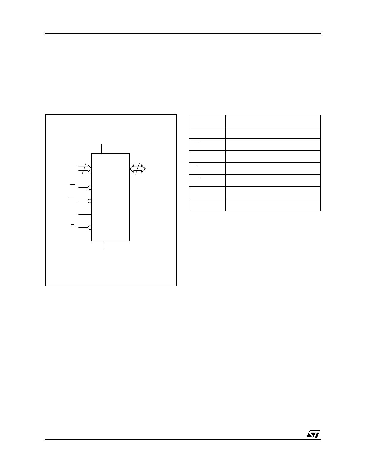
Figure 2. Logic Diagram . . . . . . . . . . . . . . . . . . . . . . . . . . . . . . . . . . . . . . . . . . . . . . . . . . . . . . . . . . 4
Table 1. Signal Names . . . . . . . . . . . . . . . . . . . . . . . . . . . . . . . . . . . . . . . . . . . . . . . . . . . . . . . . . . 4
Figure 3. SO Connections. . . . . . . . . . . . . . . . . . . . . . . . . . . . . . . . . . . . . . . . . . . . . . . . . . . . . . . . . 5
Figure 4. DIP Connections . . . . . . . . . . . . . . . . . . . . . . . . . . . . . . . . . . . . . . . . . . . . . . . . . . . . . . . . 5
Figure 5. TSOP Connections . . . . . . . . . . . . . . . . . . . . . . . . . . . . . . . . . . . . . . . . . . . . . . . . . . . . . . 5
Figure 6. Block Diagram . . . . . . . . . . . . . . . . . . . . . . . . . . . . . . . . . . . . . . . . . . . . . . . . . . . . . . . . . . 6
OPERATION . . . . . . . . . . . . . . . . . . . . . . . . . . . . . . . . . . . . . . . . . . . . . . . . . . . . . . . . . . . . . . . . . . . . . . 7
Read Mode . . . . . . . . . . . . . . . . . . . . . . . . . . . . . . . . . . . . . . . . . . . . . . . . . . . . . . . . . . . . . . . . . . . . 7
Write Mode. . . . . . . . . . . . . . . . . . . . . . . . . . . . . . . . . . . . . . . . . . . . . . . . . . . . . . . . . . . . . . . . . . . . 7
Table 2. Operating Modes. . . . . . . . . . . . . . . . . . . . . . . . . . . . . . . . . . . . . . . . . . . . . . . . . . . . . . . . 7
MAXIMUM RATING. . . . . . . . . . . . . . . . . . . . . . . . . . . . . . . . . . . . . . . . . . . . . . . . . . . . . . . . . . . . . . . . . 8
Table 3. Absolute Maximum Ratings. . . . . . . . . . . . . . . . . . . . . . . . . . . . . . . . . . . . . . . . . . . . . . . . 8
DC AND AC PARAMETERS. . . . . . . . . . . . . . . . . . . . . . . . . . . . . . . . . . . . . . . . . . . . . . . . . . . . . . . . . . 9
Table 4. Operating and AC Measurement Conditions. . . . . . . . . . . . . . . . . . . . . . . . . . . . . . . . . . . 9
Figure 7. AC Measurement I/O Waveform . . . . . . . . . . . . . . . . . . . . . . . . . . . . . . . . . . . . . . . . . . . . 9
Figure 8. AC Measurement Load Circuit. . . . . . . . . . . . . . . . . . . . . . . . . . . . . . . . . . . . . . . . . . . . . . 9
Table 5. Capacitance . . . . . . . . . . . . . . . . . . . . . . . . . . . . . . . . . . . . . . . . . . . . . . . . . . . . . . . . . . . 10
Table 6. DC Characteristics . . . . . . . . . . . . . . . . . . . . . . . . . . . . . . . . . . . . . . . . . . . . . . . . . . . . . 10
Figure 9. Address Controlled, Read Mode AC Waveforms . . . . . . . . . . . . . . . . . . . . . . . . . . . . . . 11
Figure 10.Chip Enable or Output Enable Controlled, Read Mode AC Waveform s . . . . . . . . . . . . . 11
Figure 11.Chip Enable Controlled, Standby Mode AC Waveform s. . . . . . . . . . . . . . . . . . . . . . . . . 12
Table 7. Read and Standby Mode AC Characteristics . . . . . . . . . . . . . . . . . . . . . . . . . . . . . . . . . 13
Figure 12.Write Enable Controlled, Write AC Waveforms . . . . . . . . . . . . . . . . . . . . . . . . . . . . . . . . 14
Figure 13.Chip Enable Controlled, Write AC Waveforms . . . . . . . . . . . . . . . . . . . . . . . . . . . . . . . . 14
Table 8. Write Mode AC Characteristics . . . . . . . . . . . . . . . . . . . . . . . . . . . . . . . . . . . . . . . . . . . . 15
Figure 14.E1
Figure 15.E2 Controlled, Low V
Table 9. Low V
Controlled, Low VCC Data Retention AC Waveforms . . . . . . . . . . . . . . . . . . . . . . . . 16
Data Retention AC Waveforms . . . . . . . . . . . . . . . . . . . . . . . . 16
CC
Data Retention Characteristics. . . . . . . . . . . . . . . . . . . . . . . . . . . . . . . . . . . . .16
CC
PACKAGE MECHANICAL . . . . . . . . . . . . . . . . . . . . . . . . . . . . . . . . . . . . . . . . . . . . . . . . . . . . . . . . . . 17
Figure 16.SO32 - 32 lead Plastic Small Outline, Package Outline . . . . . . . . . . . . . . . . . . . . . . . . . 17
Table 10. SO32 - 32 lead Plastic Small Outline, Package Mechanic al Data. . . . . . . . . . . . . . . . . . 17
Figure 17.PDIP32 - 32 pin Plastic DIP, 600 mils width, Package Outline . . . . . . . . . . . . . . . . . . . . 18
Table 11. PDIP32 - 32 pin Plastic DIP, 600 mils width, Package Mechanical Data . . . . . . . . . . . . 18
Figure 18.TSOP32 - 32-lead Thin Small Outline Package, 8x13.4m m , Package Outline. . . . . . . . 19
2/23

M68AF127B
Table 12. TSOP32 - 32-lead Thin Small Outline Package, 8x13.4mm , Packa ge Mechan ical
Data. . . . . . . . . . . . . . . . . . . . . . . . . . . . . . . . . . . . . . . . . . . . . . . . . . . . . . . . . . . . . . . . . 19
Figure 19.TSOP32 - 32 lead Plastic Thin Small Outline, 8x20mm, Package Outli ne . . . . . . . . . . . 20
Table 13. TSOP32 - 32 lead Plastic Thin Small Outline, 8x20mm, Package M echanical Data . . . 20
PART NUMBERING . . . . . . . . . . . . . . . . . . . . . . . . . . . . . . . . . . . . . . . . . . . . . . . . . . . . . . . . . . . . . . . 21
Table 14.Ordering Information Scheme . . . . . . . . . . . . . . . . . . . . . . . . . . . . . . . . . . . . . . . . . . . . . 21
REVISION HISTORY. . . . . . . . . . . . . . . . . . . . . . . . . . . . . . . . . . . . . . . . . . . . . . . . . . . . . . . . . . . . . . . 22
Table 15. Document Revision History. . . . . . . . . . . . . . . . . . . . . . . . . . . . . . . . . . . . . . . . . . . . . . . 22
3/23
M68AF127B
SUMMARY DESCRIPTION
The M68AF127B is a 1Mbit (1,048,576 bit) CMOS
SRAM, organized as 131,072 words by 8 bits. The
device features fully static operation requiring no
external clocks or timing strobes, with equal address access and cycle times. It requires a single
4.5 to 5.5V supply.
Figure 2. Logic Diagram Table 1. Signal Names
This device has an automatic power-down feature,
reducing the power consumption by over 99%
when deselected.
The M68AF127B is available in SO32, PDIP32,
TSOP32 (8x13.4mm) and TSOP32 (8x20mm)
packages.
A0-A16 Address Inputs
A0-A16
W
E1
E2
V
CC
17
M68AF127B
G
V
SS
8
DQ0-DQ7
AI05472B
DQ0-DQ7 Data Input/Output
E1
E2 Chip Enable
G
W
V
CC
V
SS
Chip Enable
Output Enable
Write Enable
Supply Voltage
Ground
4/23
M68AF127B
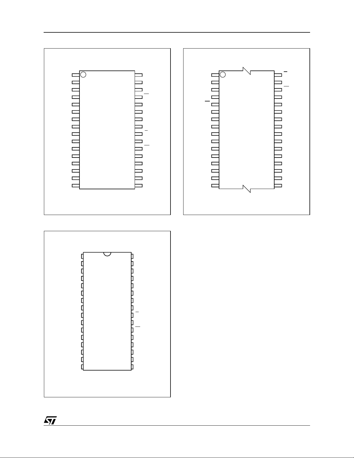
Figure 3. SO C on nec ti ons
NC
A16
A14
A12
A7
A6
A5
A4
A3
A2
A1
A0
DQ0
DQ1
DQ2
V
SS
1
8
M68AF127B
9
16 17
32
25
24
AI07270B
V
CC
A15
E2
W
A13
A8
A9
A11
G
A10
E1
DQ7
DQ6
DQ5
DQ4
DQ3
Figure 5. TSOP Connection s
A11
A9
A8
A13
E2
A15
V
CC
NC
A16
A14
A12
A7
A6
A5
A4 A3
1
W
8
M68AF127B
9
16 17
32
25
24
AI05473d
G
A10
E1
DQ7
DQ6
DQ5
DQ4
DQ3
V
SS
DQ2
DQ1
DQ0
A0
A1
A2
Figure 4. DIP C on ne ctions
NC
1
A16
2
A14
3
A12
4
A7
5
A6
6
A5
7
8
A4
A3
A2
A1
A0
DQ0
DQ1
DQ2
V
SS
M68AF127B
9
10
11
12
13
14
15
16
32
31
30
29
28
27
26
25
24
23
22
21
20
19
18
17
AI07203B
V
CC
A15
E2
W
A13
A8
A9
A11
G
A10
E1
DQ7
DQ6
DQ5
DQ4
DQ3
5/23
M68AF127B
Figure 6. Block Diagram
A16
A7
ROW
DECODER
MEMORY
ARRAY
E1
E2
DQ7
DQ0
Ex
W
G
I/O CIRCUITS
COLUMN
DECODER
A0 A6
AI05471
6/23
OPERATION
The M68AF127B has a Chip Enable power down
feature which invokes an automatic standby mode
whenever Chip Enable is de-asserted (E1
or Chip Select is asserted (E2 = Low). An Output
Enable (G
) signal provides a high-speed, tri-state
Read Mode
The M68AF127B is in the Read mode whenever
Write En able (W
Low, Chip Enable (E1
) is High with Output Enable (G)
) is asserted and Chip Select
(E2) is de-asserted. This provid es access to dat a
from eight of the 1,048,576 loca tions in the static
memory array, specified by the 17 address inputs.
Valid data will be available at the eight output pins
Write Mode
The M68AF127B is in the Write mode whenever
and E1 pins are Low and the E2 pin is High.
the W
Either the Chip Enable input (E1
able input (W
) must be de-asserted during Ad-
) or the Write En-
dress transitions for subsequent write cycles.
Write begins with the concurrence of E1
tive w ith W
low. Therefore, address setup time is
referenced to Write Enable and Chip Enable as
t
AVWL
and t
, respectively, and is determined
AVEH
by the latter occurring edge.
= High),
being ac-
M68AF127B
control, allowing fast read/write cycles to be
achieved with the common I/O data bus. Operational modes are determined by device control inputs W
Modes table (Table 2).
within t
ing G
put Enable access times are not met, data access
will be measured from the limiting parameter
(t
may be indeterminate at t
lines will always be valid at t
The Write cycle can be terminated by the earlier
rising edge of E1
If the Output is enabled (E1
G
pedance within t
be taken to avoid bus contention in this type of operation. Data input must be valid for t
the rising edge of Write Enable, or for t
the rising edge of E1
remain valid for t
and E1 as summarized in the Operating
after the last stable addres s, provid-
AVQV
is Low and E1 is Low. If Chip Enable or Out-
ELQV
or t
) rather than the address. Data out
GLQV
ELQX
and t
AVQV
GLQX
.
, but data
, or W.
= Low, E2 = High and
= Low), then W will return the outputs to high im-
of its falling edge. Care must
WLQZ
before
DVWH
before
DVEH
, whichever occurs first, and
WHDX
or t
EHDX
.
Table 2. Operating Modes
Operation E1 E2 W G DQ0-DQ7 Power
Read
Read
Write
Deselect
Deselect X
Note: X = VIH or VIL.
V
IL
V
IL
V
IL
V
IH
V
IH
V
IH
V
IH
X X X Hi-Z
V
IL
V
IH
V
IH
V
IL
X X Hi-Z
V
IH
V
IL
X Data Input
Hi-Z
Data Output
Active (I
Active (I
Active (I
Standby (I
Standby (I
CC
CC
CC
SB
SB
)
)
)
)
)
7/23

M68AF127B
MAXIMUM RATING
Stressing the device above the rating l isted in the
“Absolute Maximum Ratings” table may cause
permanent damage to the device. These are
stress ratings only and operation of the device at
these or any other conditions above those indicated in the Operating sections of this specification is
Table 3. Absolute Maximum Ratings
Symbol Parameter Value Unit
(1)
I
O
T
A
T
STG
V
CC
(2)
V
IO
P
D
Note: 1. One output at a time, not to exce ed 1 second duration.
2. Up to a maximum opera ting V
Output Current 20 mA
Ambient Operating Temperature –55 to 125 °C
Storage Temperature –65 to 150 °C
Supply Voltage –0.5 to 6.5 V
Input or Output Voltage
Power Dissipation 1 W
of 6.0V only.
CC
not implied. Exposure to Absol ute Max imum Ra ting conditions for extended periods may affect device reliability. Refer also to the
STMicroelectronics SURE Program and other relevant quality documents.
–0.5 to V
CC
+0.5
V
8/23

DC AND AC PARAMETERS
This section summarizes the operating and measurement conditions, as well as the DC and AC
characteristics of the device. The parameters in
the following DC and AC Characteristic tables are
derived from tests performed under the Meas ure-
Table 4. Operating and AC Measurement Conditions
Parameter M68AF127B
V
Supply Voltage
CC
Ambient Operating Temperature
M68AF127B
ment Conditions listed in t he relevant tables. Designers should check that the operating conditions
in their projects match the measurement conditions when using the quoted parameters.
4.5 to 5.5V
Range 1 0 to 70°C
Range 6 –40 to 85°C
Load Capacitance (C
Output Circuit Protection Resis tance (R
Load Resistance (R
)
L
)
1
)
2
100pF
3.0kΩ
3.1kΩ
Input Rise and Fall Times 1ns/V
Input Pulse Voltages
Input and Output Timing Ref. Voltages
Output Transition Timing Ref. Voltages
V
RL
0 to V
CC
V
/2
CC
= 0.3VCC; VRH = 0.7V
Figure 7. AC Measurement I/O Waveform Figure 8. AC Measurement Load Circuit
V
CC
I/O Timing Reference Voltage
V
CC
0V
Output Transition Timing Reference Voltage
V
CC
0V
VCC/2
0.7V
0.3V
AI04831
DEVICE
UNDER
TEST
R
CC
CC
CL includes JIG capacitance
R
1
OUT
C
L
2
CC
AI05814
9/23

M68AF127B
Table 5. Capacitance
Symbol
C
C
OUT
Note: 1. Sampled only, not 100% tested.
2. At T
Input Capacitance on all pins (except DQ)
IN
Output Capacitance
= 25°C, f = 1MHz, VCC = 3.0V.
A
Parameter
(1,2)
Table 6. DC Characteristics
Symbol Parameter Test Condition Min Typ Max Unit
V
I
CC1
I
CC2
I
LO
I
(1,2)
Supply Current
(3)
Operating Supply Current
I
Input Leakage Current
LI
(4)
Output Leakage Current
Standby Supply Current CMOS
SB
= 5.5V, f = 1/t
CC
I
OUT
= 5.5V, f = 1MHz,
V
CC
0V ≤ V
0V
V
= 5.5V, E1 ≥ V
CC
E2 ≤ 0.2V, f=0
= 0mA
I
= 0mA
OUT
≤ V
OUT
IN
≤ V
≤ V
AVAV
CC
CC
,
CC
– 0.2V,
Test
Condition
V
= 0V
IN
V
= 0V
OUT
Min Max Unit
6pF
8pF
55 7.5 20 mA
70 6.0 15 mA
2mA
–1 1 µA
–1 1 µA
2.5 15 µA
V
V
V
V
Note: 1. Average AC current, cyc l ing at t
Input High Voltage 2.2
IH
Input Low Voltage –0.3 0.8 V
IL
Output High Voltage
OH
Output Low Voltage
OL
= VIL, E2 = VIH, VIN = VIH or VIL.
2. E1
≤ 0.2V or E2 ≥ VCC –0.2V, VIN ≤ 0.2V or VIN ≥ VCC –0.2V .
3. E1
4. Output disabled.
AVAV
minimum.
I
= –1mA
OH
I
= 2.1mA
OL
V
+ 0.3
CC
2.4 V
0.4 V
V
10/23

Figure 9. Address Controlled, Read Mode AC Waveforms
tAVAV
M68AF127B
A0-A16
tAVQV tAXQX
DQ0-DQ7
Note: E1 = Low, E2 = High, G = Lo w, W = High.
VALID
DATA VALID
Figure 10. Chip Enable or Output Enable Controlled, Read Mode AC Waveforms
tAVAV
A0-A16
tAVQV tAXQX
tELQV
E1
E2
VALID
AI05474
tEHQZ
G
DQ0-DQ7
Note: Write Enable (W) = High.
tELQX
tGLQX
tGLQV
tGHQZ
VALID
AI05476
11/23

M68AF127B
Figure 11. Chip Enable Controlled, Standby Mode AC Waveform s
E1
E2
I
I
CC
SB
tPU
50%
tPD
AI05477
12/23

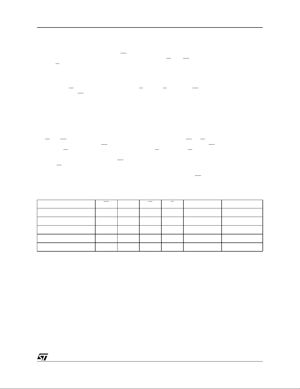
Table 7. Read and Standby Mode AC Characteristics
Symbol Parameter
t
t
AVQV
t
AXQX
t
EHQZ
t
ELQV
t
ELQX
t
GHQZ
t
GLQV
t
GLQX
AVAV
Read Cycle Time Min 55 70 ns
Address Valid to Output Valid Max 55 70 ns
(1)
Data hold from address change Min 5 5 ns
(2,3)
Chip Enable High to Output Hi-Z Max 20 25 ns
Chip Enable Low to Output Valid Max 55 70 ns
(1)
Chip Enable Low to Output Transition Min 5 5 ns
(2,3)
Output Enable High to Output Hi-Z Max 20 25 ns
Output Enable Low to Output Valid Max 25 35 ns
(2)
Output Enable Low to Output Transition Min 5 5 ns
M68AF127B
M68AF127B
Unit
55 70
t
PD
t
PU
Note: 1. Test conditions assume t ransition ti m i ng refere nce level = 0. 3VCC or 0.7VCC.
2. At any gi v en tempera tu re and voltage condition, t
3. These parameters are defined as the time at which the outputs achieve the open circuit conditions and are not referenced to output
Chip Enable or UB/LB High to Power Down Max 55 70 ns
Chip Enable or UB/LB Low to Power Up Min 0 0 ns
voltage lev els.
is less than t
GHQZ
GLQX
and t
is less than t
EHQZ
for any given device.
ELQX
13/23

M68AF127B
Figure 12. Write Enable Controlled, Write AC Waveforms
tAVAV
A0-A16
tAVEL
E1
E2
tAVWL
W
tWLQZ
DQ0-DQ7
VALID
tAVWH
tELWH
tWLWH
Figure 13. Chip Enable Controlled, Write AC Waveforms
tWHAX
tWHQX
tWHDX
DATA INPUT
tDVWH
AI05478
A0-A16
E1
E2
W
DQ0-DQ7
tAVWL
tAVEL
tAVAV
VALID
tAVEH
tWLEH
tELEH
tEHAX
tEHDX
DATA INPUT
tDVEH
AI05479
14/23

M68AF127B
Table 8. Write Mode AC Characteristics
Symbol Parameter
t
AVAV
t
AVEH
t
AVEL
t
AVWH
t
AVWL
t
DVEH
t
DVWH
t
EHAX
t
EHDX
t
ELEH
t
ELWH
t
WHAX
t
WHDX
t
WHQX
t
WLEH
t
WLQZ
t
WLWH
Note: 1. At any given temperature a nd voltage condition, t
2. These parameters are defined as the time at which the outputs achieve the open circuit conditions and are not referenced to output
Write Cycle Time Min 55 70 ns
Address Valid to Chip Enable High Min 45 60 ns
Address valid to Chip Enable Low Min 0 0 ns
Address Valid to Write Enable High Min 45 60 ns
Address Valid to Write Enable Low Min 0 0 ns
Input Valid to Chip Enable High Min 25 30 ns
Input Valid to Write Enable High Min 25 30 ns
Chip Enable High to Address Transition Min 0 0 ns
Chip enable High to Input Transition Min 0 0 ns
Chip Enable Low to Chip Enable High Min 45 60 ns
Chip Enable Low to Write Enable High Min 45 60 ns
Write Enable High to Address Transition Min 0 0 ns
Write Enable High to Input Transition Min 0 0 ns
(1)
Write Enable High to Output Transition Min 5 5 ns
Write Enable Low to Chip Enable High Min 45 60 ns
(1,2)
Write Enable Low to Output Hi-Z Max 20 20 ns
Write Enable Low to Write Enable High Min 45 60 ns
voltage lev els.
is less than t
WLQZ
for any given devi ce.
WHQX
M68AF127B
55 70
Unit
15/23

M68AF127B
Figure 14. E1 C ont ro l led , Lo w VCC Data Retention AC Waveforms
5.5V
VCC 4.5V
V
> 2.0V
DR
E1
Figure 15. E2 Controlled, Low V
5.5V
VCC 4.5V
V
> 2.0V
DR
E2
DATA RETENTION MODE
tCDR
E1 ≥ V
Data Retention AC Waveforms
CC
DATA RETENTION MODE
tCDR
– 0.2V
DR
E2 ≤ 0.2V
tR
AI07204
tR
AI07205B
Table 9. Low V
Data Retention Characteristics
CC
Symbol Parameter Test Condition Min Max Unit
V
= 2.0V, E1 ≥ V
E1
CC
≥ V
(1)
I
CCDR
t
CDR
t
R
V
DR
Note: 1. All other Inputs at VIH ≥ V
Supply Current (Data Retention)
(1,2)
Chip Deselected to Data Retention Time 0 ns
(2)
Operation Recovery Time
(1)
Supply Voltage (Data Retention)
–0.2V or VIL ≤ 0.2V.
2. Tested initiall y and after any design or proc ess that may affect these paramete rs.
3. No input may exceed V
CC
CC
+0.2V.
E2 ≤ 0.2V, f = 0
–0.2V or E2 ≤ 0.2V, f = 0
CC
–0.2V or
CC
t
is Read cycle time.
AVAV
4.5 µA
t
AVAV
2.0 V
ns
16/23

PACKAGE ME CHANICAL
Figure 16. SO32 - 32 lead Plastic Small Outline, Package Outline
D
M68AF127B
16
17 32
B
e
1
E
E1
A2
A1
A
CP
L1
SO-C
Note: Drawing is not to scale.
Table 10. SO32 - 32 lead Plastic Small Outline, Package Mechan ical Data
Symbol
Typ Min Max Typ Min Max
B 0.36 0.51 0.014 0.020
A 3.00 0.118
millimeters inches
C
L
A1 0.10 0.004
A2 2.57 2.82 0.101 0.111
C 0.15 0.30 0.006 0.012
CP 0.10 0.004
D 20.14 20.75 0.793 0.817
E 11.18 11.43 0.440 0.450
E1 13.87 14.38 0.546 0.566
e 1.27 – – 0.050 – –
L 0.58 0.99 0.023 0.039
L1 1.19 1.60 0.047 0.063
N32 32
17/23

M68AF127B
Figure 17. PDIP32 - 32 pin Plastic DIP, 600 mils width, Package Outline
A2
A1AL
b1 b e
α
c
eA
D2
D
S
N
E1 E
1
Note: Drawing is not to scale.
PDIP-C
Table 11. PDIP32 - 32 pin Plastic DIP, 600 mils width, Package Mechanical Data
Symbol
Typ Min Max Typ Min Max
A 4.83 0.190
A1 0.38 0.015
A2 3.81 0.150
millimeters inches
b 0.41 0.53 0.016 0.021
b1 1.14 1.65 0.045 0.065
c 0.23 0.38 0.009 0.015
D 41.78 42.29 1.645 1.665
eA 15.24 – – 0.600 – –
e 2.54 – – 0.100 – –
E 15.24 15.88 0.600 0.625
E1 13.46 13.97 0.530 0.550
L 3.05 3.56 0.120 0.140
S 1.65 2.21 0.065 0.087
α 0° 15° 0° 15°
N32 32
18/23

Figure 18. TSOP32 - 32-lead Thin Small Outline Package, 8x13.4m m, Packag e Outline
A2
M68AF127B
1
N
e
E
B
N/2
D1
D
DIE
A
CP
C
TSOP-a
Note: Drawing is not to scale.
LA1
α
Table 12. TSOP32 - 32-lead Thin Small Outline Package, 8x13.4 mm , Packa ge M echanic al Data
Symbol
Typ Min Max Typ Min Max
A 1.20 0.0472
millimeters inches
A1 0.05 0.15 0.0020 0.0059
A2 0.91 1.05 0.0358 0.0413
B 0.22 0.0087
C 0.10 0.21 0.0039 0.0083
CP 0.10 0.0039
D 13.40 – – 0.5276 – –
D1 11.80 – – 0.4646 – –
E 8.00 – – 0.3150 – –
e 0.50 – – 0.0197 – –
L 0.40 0.60 0.0157 0.0236
α 0° 5° 0° 5°
N32 32
19/23

M68AF127B
Figure 19. TSOP32 - 32 lead Plastic Thin Small Outline, 8x20mm, Package Outlin e
A2
1
N
e
E
B
N/2
D1
D
DIE
A
CP
C
TSOP-a
Note: Drawing is not to scale.
LA1
α
Table 13. TSOP32 - 32 lead Plastic Thin Small Outline, 8x20mm, Pac kage Mechanical Data
millimeters inches
Symbol Typ Min Max Typ Min Max
A 1.200 0.0472
A1 0.050 0.150 0.0020 0.0059
A2 0.950 1.050 0.0374 0.0413
B 0.170 0.250 0.0067 0.0098
C 0.100 0.210 0.0039 0.0083
CP 0.100 0.0039
D 19.800 20.200 0.7795 0.7953
D1 18.300 18.500 0.7205 0.7283
e 0.500 – – 0.0197 – –
E 7.900 8.100 0.3110 0.3189
L 0.500 0.700 0.0197 0.0276
α 0° 5° 0° 5°
N32 32
20/23

PART NUMBERING
Table 14. Ordering Information Scheme
Example: M68AF127 B L 55 MC 6 T
Device Type
M68
Mode
A = Asynchronous
Operating Voltage
F = 4.5 to 5.5V
Array Organization
127 = 1Mbit (128K x8)
Option 1
B = 2 Chip Enable
Option 2
L = L-Die
M = M-Die
M68AF127B
Speed Class
55 = 55ns
70 = 70ns
Package
MC = SO32
B = PDIP32
NK = TSOP32 8x13.4mm
N = TSOP32 8x20mm
Operative Temperature
1 = 0 to 70°C
6 = –40 to 85°C
Shipping
T = Tape & Reel Packing
For a list of available options (e.g., Speed, Package) or for further information on any aspect of this device,
please contact the STMicroelectronics Sales Office nearest to you.
21/23

M68AF127B
REVISION HISTORY
Table 15. Document Revision History
Date Version Revision Details
August 2001 1.0 First Issue.
18-Oct-2001 2.0 SO32 Package Mechanical and Data added (Figure 1, 3 and 16, Table 10).
29-Nov-2001 3.0 Note removed from Ordering Information Scheme.
06-Mar-2002 4.0 Document status changed to Data Sheet.
17-May-2002 5.0 Document globally revised.
31-May-2002 6.0
09-Sep-2002 6.1
02-Oct-2002 6.2 Title and header layout modified.
09-Oct-2002 6.3 Datasheet number simplified.
16-Apr-2003 6.4
08-Aug-2003 6.5
21-Aug-2003 6.6 TSOP Package connections modified (Figure 5).
PDIP32 Package added (Figure 1, 4 and 17, Table 11).
Chip Enable Low V
TSOP32 8x13.4mm and TSOP32 8x20mm packages added (Figure 1, 5, 18 and 19,
Table 12, 13 and 14).
Commercial code clarified.
Label corrected on “E2 Controlled, Low V
TSOP Package connections modified (Figure 5).
Test conditions for ICCDR modified in Table 9, Low V
Characteristics.
Data Retention clarified (Figure 14 and 15, Table 9).
CC
Data Retention AC Waveforms” figure.
CC
Data Retention
CC
24-Sep-2004 7
Document structure modified:
– Chapter OPERATION moved before chapter MAXIMUM RATING.
– AC Characteristics Tables and waveforms moved to the DC/AC PARAMETERS
section.
ad tPD updated in Table 7.
t
PU
22/23

M68AF127B
Information furnished is believed to be accurate and reliable. However, STMicroelectronics a ssumes no responsibility fo r the c onsequences
of use of such information nor for any infringement of patents or other rights of third parties which may result from its use. No license is granted
by implication or otherwise under any patent or patent rights of STMicroelectronics. Specifications mentioned in this publication are subject
to change without notice. This publication supersedes and replaces all information previously supplied. STMicroelectronics products are not
authori zed for use as crit i cal compon ents in life support devic es or systems without ex press written approval of STMicroel ectronics.
The ST logo is a registered trademark of STM i croelectr onics.
All other nam es are the pro perty of their respectiv e owners
© 2004 STMi croelectronics - All rights reser ved
Australi a - Belgium - B razil - Canada - China - Czech Republi c - Finland - F rance - Germ any - Hong Ko ng - India - Isra el - It aly - Japan -
Malaysia - M al ta - Morocco - Singapore - Spain - Sweden - Swit zerland - Un i ted Kingdom - United Sta tes of Americ a
STMicroelectron ics group of com panies
www.st.com
23/23
 Loading...