

1/38
PRELIMINARY DATA
October 1999
This is preliminary information on a new product now in development or undergoing evaluation. Details are subject to change without notice.
M59DR032A
M59DR032B
32 Mbit (2Mb x16, Dual Bank, Page) Low Voltage Flash Memory
■ SUPPLY VOLTAGE
–V
DD
= V
DDQ
= 1.65V to 2.2V: for Program,
Erase and Read
–V
PP
= 12V: o ptional Supply Voltage for fast
Program and Erase
■ ASYNCHRONOUS PAGE MODE READ
– Page Width: 4 words
– Page Access: 35ns
– Random Access: 100ns
■ PROGRAMMING TIME
– 10µs by Word typical
– Double Word Programming Option
■ MEMORY BLOCKS
– Dual Bank Memory Array: 4 Mbit - 28 Mbit
– Parameter Blo cks (Top or Bottom location)
– Main Blocks
■ DUAL BANK OPERATIONS
– Read within one Bank while Program or
Erase within the other
– No delay between Read and Write operations
■ BLOCK PROTECTION/UNPROTECTION
– All Blocks protected at Power Up
– Any combination of Blocks can be protected
–WP
for Block Locking
■ COMMON FLASH INTERFACE (CFI)
■ 64 bit SECURITY CODE
■ ERASE SUSPEND and RESUME MODES
■ 100,000 PROGRAM/ERASE CYCL ES per
BLOCK
■ 20 YEARS DATA RETEN TION
– Defectivity below 1ppm/year
■ ELECTRONIC SIGNATURE
– Manufacturer Code: 20h
– Device Code, M59DR032A: A0h
– Device Code, M59DR032B: A1h
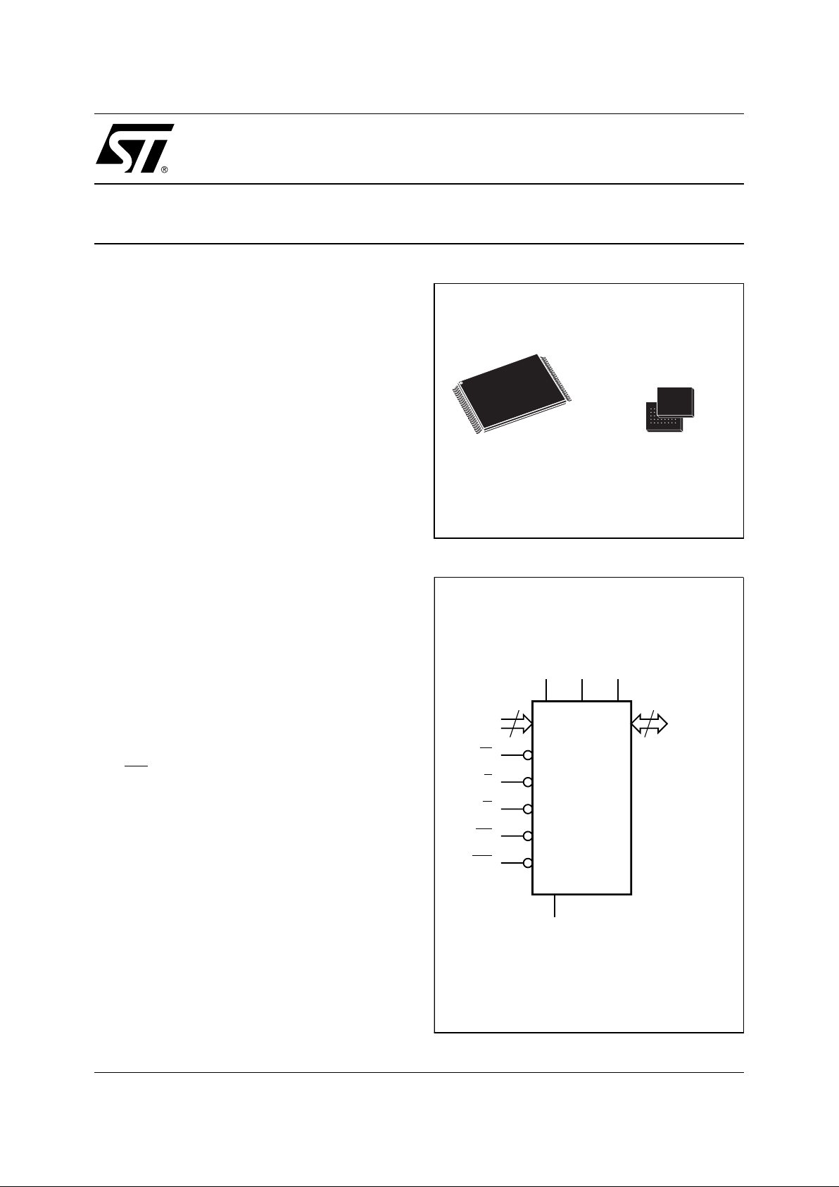
BGA
TSOP48 (N)
12 x 20mm
FBGA48 (ZB)
8 x 6 solder balls
Figure 1. Logic Diagram
AI02544B
21
A0-A20
W
DQ0-DQ15
V
DD
M59DR032A
M59DR032B
E
V
SS
16
G
RP
WP
V
DDQVPP
M59DR032A, M59DR032B
2/38
Figure 2A. FBGA Connections (Top View)
AI02532C
C
B
A
87654321
E
D
F
A4
A7V
PP
A8A11
A13
A0EDQ8DQ5DQ14A16
V
SS
DQ0DQ9DQ3DQ6DQ15V
DDQ
DQ1DQ10V
DD
DQ7V
SS
DQ2
A2
A5A17WA10
A14
A1A3A6A20DUA9A12A15
RP A18
DQ4
DQ13
G
DQ12
DQ11
WP A19
Figure 2B. TSOP Connections
DQ3
DQ9
DQ2
A6
DQ0
W
A3
NC
DQ6
A8
A9
DQ13
A17
A10 DQ14
A2
DQ12
DQ10
DQ15
V
DD
DQ4
DQ5
A7
DQ7
V
PP
WP
AI02533B
M59DR032A
M59DR032B
12
1
13
24 25
36
37
48
DQ8
A20
A19
A1
A18
A4
A5
DQ1
DQ11
G
A12
A13
A16
A11
V
DDQ
A15
A14
V
SS
E
A0
RP
V
SS
Table 1. Signal Names
A0-A20 Address Inputs
DQ0-DQ15 Data Input/Outputs, Command Inputs
E
Chip Enable
G
Output Enable
W
Write Enable
RP
Reset/Power Down
WP
Write Protect
V
DD
Circuitry Supp ly Voltage
V
DDQ
Input/Output Buffers Supply Voltage
V
PP
Optional Supply Voltage for
Fast Program & Erase
V
SS
Ground
NC Not Connected Internally
DU Don’t use as internally connected
3/38
M59DR032A, M59DR032B
DESCRIPTION
The M59DR032 is a 32 Mbit non-volatile Flash
memory that m ay be erased electrically a t block
level and programmed i n-system on a Word-byWord basis using a 1.65V to 2.2V V
DD
supply for
the circuitry. For Program and Erase operations
the necessary high voltages are g enerated internally. The device supports asynchronous page
mode from all the blocks of the memory array.
The array matrix organization allows each block to
be erased and reprogrammed without affecting
other blocks. All blocks are protected against programming and erase at Power Up. Blocks can be
unprotected to make changes in the application
and then reprotected.
Instructions for Read/Reset, Auto Select, Write
Configuration Register, Programming, Block
Erase, Bank Erase, Erase Suspend, Erase Resume, Block Protect, Block Unprotect, Block Locking, CFI Query, are written to the memory through
a Command Interface using standard microprocessor write timings.
The device is offered in TSOP48 (12 x 20 mm)
and in FBGA48 0.75 mm ball pitch packages.
When shipped all bits of the M59DR032 device are
at the logical level ‘1’.
Organization
The M59DR032 is organized as 2Mb x16 bits. A0A20 are the address lines, DQ0-DQ15 are the
Data Input/Output. Memory control is provided by
Chip Enable E
, Output Enable G and Write Enable
W
inputs.
Reset RP
is used to reset all the memory circuitry
and to set the chip in power down mode if this
function is enabled by a proper setting of the Configuration Register. Erase and Program operations
are controlled by an internal Program/Erase Controller (P/E.C.). Status Register data output on
DQ7 provides a Data Polling signal, DQ6 and DQ2
provide Toggle signals and DQ5 provides error bit
to indicate the state of the P/E.C operations.
Memory Blocks
The device features asymmetrically blocked architecture. M59DR032 has an array of 71 blocks and
is divided into two banks A and B, prov iding D ual
Bank operations. While programming or erasing in
Bank A, read operations are possible into Bank B
or vice versa. The memory also features an erase
suspend allowing to read or program in another
block within the same bank. Once suspended the
erase can be resumed. The Bank Size and Sectorization are summarized in Table 7. Parameter
Blocks are located at the top of the m emory address space for the M59DR032A, and at the bo ttom for the M59DR032B. The memory maps are
shown in Tables 3, 4, 5 and 6.
The Program and Erase operation s are managed
automatically by the P/E.C. Block protection
against Program or Erase provides additional data
security. All blocks are protected at Power Up. Instructions are provided to protect or unprotect any
block in the application. A second register locks
the protection status while WP
is low (see B lock
Locking description). The Reset command does
not affect the configurati on of unprotected blo cks
and the Configuration Register status.
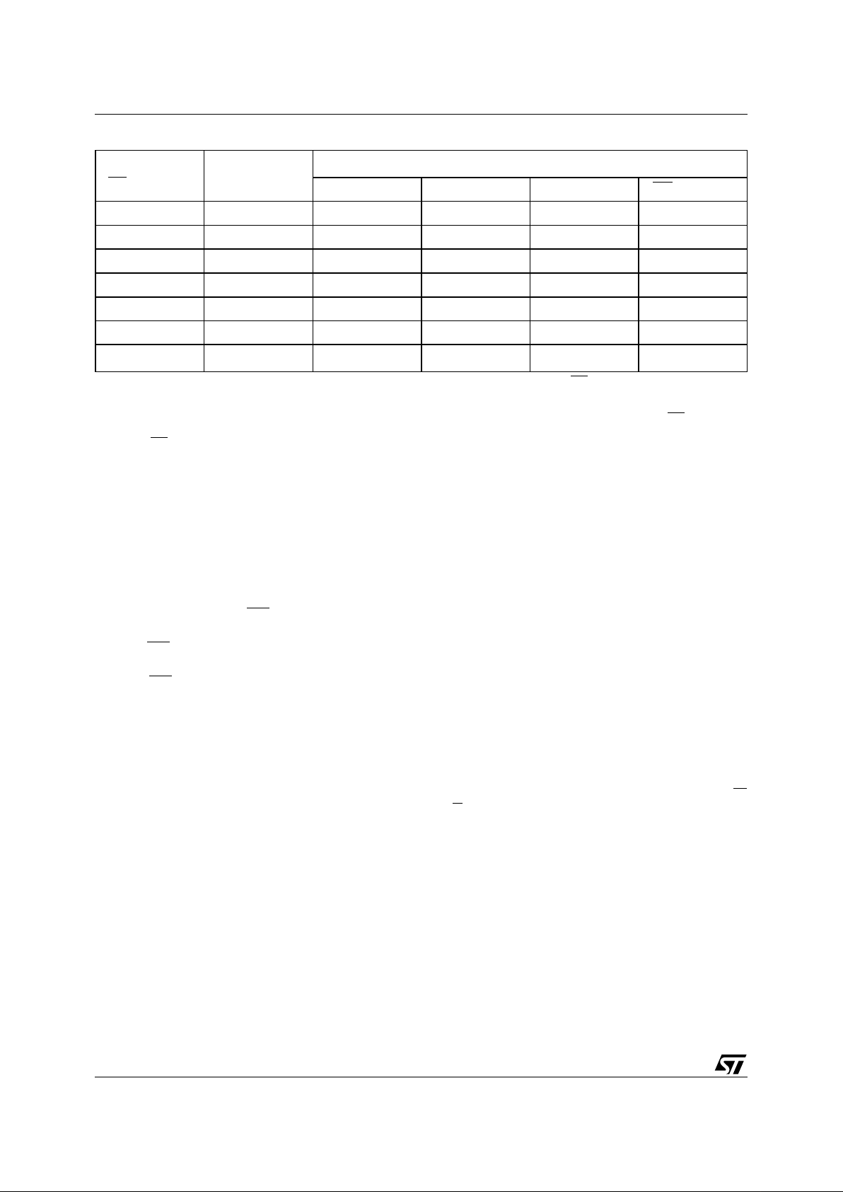
Table 2. Absolute Maximum Ratings
(1)
Note: 1. Except for th e rating "O perating T em perature R ange", stresses abo ve those listed in the T able "Absol ute Maxim um Ratings" may
cause permanent damage to the device. These are stress ratings only and operation of the device at these or any other conditions
above those indi cated in t he Operating sect i ons of thi s specifi cation i s not impl i ed. Exposure to Absolute M aximum Rating c onditions for extended per iods may aff ect device reliabilit y. Refer also to the STMicroel ectronics SURE Program an d other relevan t qual ity docum en ts .
2. Depends on range.
3. Minim um Voltage may undershoot to –2V duri ng transit i on and for less than 20ns.
Symbol Parameter Value Unit
T
A
Ambient Operating Temperature
(2)
–40 to 85 °C
T
BIAS
Temperature Under Bias –40 to 125 °C
T
STG
Storage Temperature –55 to 155 °C
V
IO
(3)
Input or Output Voltage
–0.5 to V
DDQ
+0.5
V
V
DD
, V
DDQ
Supply Voltage –0.5 to 2.7 V
V
PP
Program Voltage –0.5 to 13 V
M59DR032A, M59DR032B
4/38
Table 3. Bank A, Top Boot Block Address
Table 4. Bank B, Top Boot Block Address
Size (KWord) Address Range
4 1FF000h-1FFFFFh
4 1FE000h-1FEFFFh
4 1FD000h-1FDFFFh
4 1FC000h-1FCFFFh
4 1FB000h-1FBFFFh
4 1FA000h-1FAFFFh
4 1F9000h-1F9FFFh
4 1F8000h-1F8FFFh
32 1F0000h-1F7FFFh
32 1E8000h-1EFFFFh
32 1E0000h-1E7FFFh
32 1D8000h-1DFFFFh
32 1D0000h-1D7FFFh
32 1C8000h-1CFFFFh
32 1C0000h-1C7FFFh
Size (KWord) Address Range
32 1B8000h-1BFFFFh
32 1B0000h-1B7FFFh
32 1A8000h-1AFFFFh
32 1A0000h-1A7FFFh
32 198000h-19FFFFh
32 190000h-197FFFh
32 188000h-18FFFFh
32 180000h-187FFFh
32 178000h-17FFFFh
32 170000h-177FFFh
32 168000h-16FFFFh
32 160000h-167FFFh
32 158000h-15FFFFh
32 150000h-157FFFh
32 148000h-14FFFFh
32 140000h-147FFFh
32 138000h-13FFFFh
32 130000h-137FFFh
32 128000h-12FFFFh
32 120000h-127FFFh
32 118000h-11FFFFh
32 110000h-117FFFh
32 108000h-10FFFFh
32 100000h-107FFFh
32 0F8000h-0FFFFFh
32 0F0000h-0F7FFFh
32 0E8000h-0EFFFFh
32 0E0000h-0E7FFFh
32 0D8000h-0DFFFFh
32 0D0000h-0D7FFFh
32 0C8000h-0CFFFFh
32 0C0000h-0C7FFFh
32 0B8000h-0BFFFFh
32 0B0000h-0B7FFFh
32 0A8000h-0AFFFFh
32 0A0000h-0A7FFFh
32 098000h-09FFFFh
32 090000h-097FFFh
32 088000h-08FFFFh
32 080000h-087FFFh
32 078000h-07FFFFh
32 070000h-077FFFh
32 068000h-06FFFFh
32 060000h-067FFFh
32 058000h-05FFFFh
32 050000h-057FFFh
32 048000h-04FFFFh
32 040000h-047FFFh
32 038000h-03FFFFh
32 030000h-037FFFh
32 028000h-02FFFFh
32 020000h-027FFFh
32 018000h-01FFFFh
32 010000h-017FFFh
32 008000h-00FFFFh
32 000000h-007FFFh
5/38
M59DR032A, M59DR032B
Table 5. Bank B, Bottom Boot Block Address
Size (KWord) Address Range
32 1F8000h-1FFFFFh
32 1F0000h-1F7FFFh
32 1E8000h-1EFFFFh
32 1E0000h-1E7FFFh
32 1D8000h-1DFFFFh
32 1D0000h-1D7FFFh
32 1C8000h-1CFFFFh
32 1C0000h-1C7FFFh
32 1B8000h-1BFFFFh
32 1B0000h-1B7FFFh
32 1A8000h-1AFFFFh
32 1A0000h-1A7FFFh
32 198000h-19FFFFh
32 190000h-197FFFh
32 188000h-18FFFFh
32 180000h-187FFFh
32 178000h-17FFFFh
32 170000h-177FFFh
32 168000h-16FFFFh
32 160000h-167FFFh
32 158000h-15FFFFh
32 150000h-157FFFh
32 148000h-14FFFFh
32 140000h-147FFFh
32 138000h-13FFFFh
32 130000h-137FFFh
32 128000h-12FFFFh
32 120000h-127FFFh
32 118000h-11FFFFh
32 110000h-117FFFh
32 108000h-10FFFFh
32 100000h-107FFFh
32 0F8000h-0FFFFFh
32 0F0000h-0F7FFFh
32 0E8000h-0EFFFFh
32 0E0000h-0E7FFFh
Table 6. Bank A, Bottom Boot Block Address
32 0D8000h-0DFFFFh
32 0D0000h-0D7FFF h
32 0C8000h-0CFFFFh
32 0C0000h-0C7FFF h
32 0B8000h-0B FFFFh
32 0B0000 h-0B7FFFh
32 0A8000h-0A FFFFh
32 0A0000 h-0A7FFFh
32 098000 h-09FFFFh
32 0 90000h-097FFFh
32 088000 h-08FFFFh
32 0 80000h-087FFFh
32 078000 h-07FFFFh
32 0 70000h-077FFFh
32 068000 h-06FFFFh
32 0 60000h-067FFFh
32 058000 h-05FFFFh
32 0 50000h-057FFFh
32 048000 h-04FFFFh
32 0 40000h-047FFFh
Size (KWord) Address Range
32 038000h-03FFFFh
32 030000h-037FFFh
32 028000h-02FFFFh
32 020000h-027FFFh
32 018000h-01FFFFh
32 010000h-017FFFh
32 008000h-00FFFFh
4 007000h-007FFFh
4 006000h-006FFFh
4 005000h-005FFFh
4 004000h-004FFFh
4 003000h-003FFFh
4 002000h-002FFFh
4 001000h-001FFFh
4 000000h-000FFFh
M59DR032A, M59DR032B
6/38
SIGNAL DESCRIPTIONS
See Figure 1 and Table 1.
Address Inputs (A0-A20). The address inputs
for the memory array are latched during a write operation on the falling edge of Chip Enable E
or
Write Enable W
, whichever occurs last.
Data Input/Output (DQ0-DQ15). The Input is
data to be programm ed in the memory array or a
command to be written to the Command Interface
(C.I.) Both input data and commands are latc hed
on the rising edge of Write Enable W
. The Ouput
is data from the Memory Array, the Common Flash
Interface, the Electronic Signature Manufacturer
or Device codes, the Block Protection status, the
Configuration Register status or the Status Register Data Polling bit DQ7, the Toggle Bits DQ6 and
DQ2, the Error bit DQ5. The data bus is high impedance when the chip is deselected, Output Enable G
is at VIH, or RP is at VIL.
Chip Enable (E
). The Chip Enable input acti-
vates the memory control logic, input buffers, decoders and sense amplifiers. E
at VIH deselects
the memory and red uces the power consumption
to the standby level. E
can also be used to control
writing to the command register and to the memory array, while W
remains at VIL.
Output Enable (G
). The Output Enable gates the
outputs through the data buffers during a read operation. When G
is at VIH the outputs are High im-
pedance.
Write Enable (W
). This input controls writing to
the Command Register and Data latches. Data are
latched on the rising edge of W
.
Write Protect (WP
). This input gives an addition-
al hardware protection level against program or
erase when pulled at V
IL
, as described in the Block
Lock instruction description.
Reset/Power Down Input (RP
). The RP input
provides hardware reset of the memory (without
affecting the Configuration Register status ), and/
or Power Down functions, depending on the Configuration Register status. Reset/Power Down of
the memory is achieved by pulling RP
to VIL for at
least t
PLPH
. When the reset pul se is given, if the
memory is in Read, Erase Suspend Read or
Standby, it will output new valid data in t
PHQ7V1
af-
ter the rising edge of RP
. If the memory is in Erase
or Program modes, the oper ation will be aborted
and the reset recovery will take a maximum ot
t
PLQ7V
. The memory will recover from Power
Down (when enabled) in t
PHQ7V2
after the rising
edge of RP
. See Tables 25, 26 and Figure 9.
V
DD
and V
DDQ
Supply Voltage (1.65V to 2.2V).
The main power supply for all operations (Read,
Program and Erase). V
DD
and V
DDQ
must be at
the same voltage.
V
PP
Programming Voltage (11.4V to 12.6V ). Used
to provide high voltage for fast factory programming. High voltage on V
PP
pin is required to use
the Double Word Program instruction. It is also
possible to perform word program or erase instructions with V
PP
pin grounded.
V
SS
Ground. VSS is the reference for al l the vol t-
age measurements.
DEVICE OPERATIONS
The following operations can be performed using
the appropriate bus cycles: Read Array (Random,
and Page Modes), Write command, Output Disable, Standby, Reset/Power Down and Block
Locking. See Table 8.
Read. Read operations are used to output the
contents of the Memory Array, the Electronic Signature, the Status Register, the CFI, the Block
Protection Status or the Configuration Register
status. Read operation of the memory array is performed in asynchronous page mode, that provides
fast access time. Data is internally read and stored
in a page buffer. The page has a size of 4 words
and is addressed by A0-A1 address inputs. Read
operations of the Electroni c Signature, th e Status
Register, the CFI, the Block Protection Status, the
Configuration Register status and the Security
Code are performed as single asyncronous read
cycles (Random Read). Both Chip Enabl e E
and
Output Enable G
must be at VIL in order to read the
output of the memory.
Write. Write operations are u sed to give Instruc-
tion Commands to the memory or to latch Input
Data to be programmed. A write operation is initiated when Chip Enable E
and Write Enable W are
at V
IL
with Output Enable G at VIH. Addresses are
latched on the falling edge of W
or E whichever occurs last. Commands and Input Data are latched
on the rising edge of W
or E whichever occurs first.
Noise pulses of less than 5ns typical on E
, W and
G
signals do not start a write cycle.
Table 7. Bank Size and Sectorization
Bank Size Parameter Blocks Main Blocks
Bank A 4 Mbit 8 blocks of 4 KWord 7 blocks of 32 KWord
Bank B 28 Mbit - 56 blocks of 32 KWord
7/38
M59DR032A, M59DR032B
Table 8. User Bus Operations
(1)
Note: 1. X = Don’t care.
Table 9. Read Electronic Signature (AS and Read CFI instructions)
Table 10. Read Block Protection (AS and Read CFI instructions)
Table 11. Read Configuration Register (AS and Read CFI instructions)
Operation E G W RP WP DQ15-DQ0
Write
V
IL
V
IH
V
IL
V
IH
V
IH
Data Input
Output Disable
V
IL
V
IH
V
IH
V
IH
V
IH
Hi-Z
Standby
V
IH
XX
V
IH
V
IH
Hi-Z
Reset / Power Down X X X
V
IL
V
IH
Hi-Z
Block Locking
V
IL
XX
V
IH
V
IL
X
Code Device E
G W A0 A1 A7-A2
Other
Addresses
DQ15-DQ8 DQ7-DQ0
Manufacturer Code
V
IL
V
IL
V
IH
V
IL
V
IL
0 Don’t Care 00h 20h
Device Code
M59DR032A
V
IL
V
IL
V
IH
V
IH
V
IL
0 Don’t Care 00h A0h
M59DR032B
V
IL
V
IL
V
IH
V
IH
V
IL
0 Don’t Care 00h A1h
Block Status E
G W A0 A1 A20-A12 A7-A2
Other
Addresses
DQ0 DQ1 DQ15-DQ2
Protected Block
V
ILVILVIHVILVIH
Block Address 0 Don’t Care 1 0 0000h
Unprotected Block
V
ILVILVIHVILVIH
Block Address 0 Don’t Care 0 0 0000h
Locked Block
V
ILVILVIHVILVIH
Block Address 0 Don’t Care X 1 0000h
RP
Function E G W A0 A1 A7-A2 Other Addresses DQ10
DQ9-DQ0
DQ15-DQ11
Reset
V
IL
V
IL
V
IH
V
IH
V
IH
0 Don’t Care 0 Don’t Care
Reset/Power Down
V
IL
V
IL
V
IH
V
IH
V
IH
0 Don’t Care 1 Don’t Care
Automatic Standby. When in Read mode, after
150ns of bus inactivity and when CMOS levels are
driving the addresses, the chip automatically enters a pseudo-standby mode where consumption
is reduced to the CMOS standby value, while outputs still drive the bus.
Power Down. The memory is in Power Down
when the Configuration Register is set for Power
Down and RP
is at VIL. The power consumption is
reduced to the Power Down level, and Outputs are
in high impedance, independent of the Chip Enable E
, Output Enable G or Write Enable W inputs.
Block Locking. Any combination of blocks can
be temporarily protected against Program or
Erase by setting the lock register and pulling WP
to VIL (see Block Lock instruction).
Dual Bank Operations. The Dual Bank allows to
read data from one bank of memory while a program or erase operation is in progress in the other
bank of the memory. Read and Write cycles can
be initiated for simultaneous operations in different
banks without any d elay. Status Register du ring
Program or Erase must be monitored using an address within the bank being modified.
Output Disa bl e . The data outputs are high impedance when the Output Enable G
is at VIH with
Write Enable W
at VIH.
Standby. The memory is in standby when Chip
Enable E
is at VIH and the P/E.C. is idle. The power consumption is reduced to the standby level
and the outputs are high impedance, independent
of the Output Enable G
or Write Enable W input s.
M59DR032A, M59DR032B
8/38
INSTRUCTIONS AND COMMANDS
Seventeen instructions are defined (see Table
14A), and the internal P /E.C. automatically handles all timing and verification of the Pr ogram and
Erase operations. The Status Register Dat a Polling, Toggle, Error bits can be read at any time, during programming or erase, to monitor the progress
of the operation.
Instructions, made up of one or more com mands
written in cycles, can be given to the Program/
Erase Controller through a Command Interface
(C.I.). The C.I. latches comma nds written to the
memory. Commands are made of address and
data sequences. Two Coded Cycles unlock the
Command Interface. They are followed by an input
command or a confirmation command. The Coded
Sequence consists of writing the dat a AAh at the
address 555h during the f irst cycle and the data
55h at the address 2AAh during the second cycle.
Instructi ons a re co mpose d of up to si x cycles. The
first two cycles input a Coded Sequence to the
Command Interface which is common to all instructions (see Table 14A). T he third cycle inputs
the instruction set-up command. Subseq uent cycles output the addressed data, Elect ronic Signature, Block Protection, Configuration Register
Status or CFI Query for Read operations. In order
to give additional data protection, the instructions
for Block Erase and Bank Erase require further
command inputs. For a Program instruction, the
fourth command cycle inputs the address and data
to be programmed. For a Double Word Programming instruction, the fourth and fifth co mmand cycles input the address and data to be
programmed. For a Block Eras e and Bank Erase
instructions, the fourth and fifth cycles input a further Coded Sequence before the Erase confirm
command on the sixth cycle. Any combination of
blocks of the same memory bank can be erased.
Erasure of a memory block may be suspended, in
order to read data from another block or to program data in another block, and then resumed.
When power is first applied the command interface
is reset to Read Array.
Command sequencing must be followed exactly.
Any invalid combination of commands will reset
the device to Read Array. The inc reased number
of cycles has been chosen to ensure maximum
data security.
Read/Reset (RD) Instruction. The Read/Reset
instruction consists of one write cycle giving the
command F0h. It can be optionally preceded by
the two Coded Cycles. Subsequent read operations will r ead the memory array a ddressed and
output the data read.
CFI Query (RCFI) Instruction. Common Flash
Interface Query mode is entered writing 98h at address 55h. The CFI data structure gives information on the device, such as the sectorization, the
command set and some el ectrical specifications.
Tables 15, 16, 17 and 18 show the addresses
used to retrieve each data. The CFI data structure
contains also a se curity area; in this section, a 64
bit unique security number is written, starting at
address 80h. This area can be accessed only in
read mode by the final user and there are no ways
of changing the code after it has been written by
ST. Write a read instruction (RD) to return to Read
mode.
Table 12. Commands
Hex Code Command
00h Bypass Reset
10h Bank Erase Confir m
20h Unlock Bypass
30h Block Erase Resume/Confirm
40h Double Word Program
60h
Block Protect, or
Block Unprotect, or
Block Lock, or
Write Configuration Register
80h Set-up Erase
90h
Read Electronic Signature, or
Block Protection Status, or
Configuration Register Status
98h CFI Query
A0h Program
B0h Erase Suspend
F0h Read Array/Reset

9/38
M59DR032A, M59DR032B
Auto Select (AS) Instruction. This instruction
uses two Coded Cycles followed by one write cycle giving the command 90h to address 555h for
command set-up. A subsequent read will output
the Manufacturer or the Device Code (Electronic
Signature), the Block Protection status or the Configuration Register status depending on the levels
of A0 and A1 (see Tables 9, 10 and 11). A7-A2
must be at V
IL
, while other address input are ig-
nored. The bank address is don’t care for this instruction. The Electronic Signature can be read
from the memory allowing programming equipment or applications to automatically match their
interface to the characteristics of M59DR032. The
Manufacturer Code is output when the address
lines A0 and A1 are at V
IL
, the Device Code is out-
put when A0 is at V
IH
with A1 at VIL.
The codes are output on DQ0-DQ7 with DQ8DQ15 at 00h. The AS instruction also allows the
access to the Block Protection Status. After giving
the AS inst ructio n, A 0 is s et to V
IL
with A1 at VIH,
while A12-A20 define t he address of the block to
be verified. A read in these conditions will output a
01h if the block is protected and a 00h if the block
is not protected.
The AS Instruction finally allows the access to the
Configuration Register status if both A0 and A1
are set to V
IH
. If DQ10 is '0' only the Reset function
is active as RP
is set to VIL (default at power-up).
If DQ10 is '1' both the Reset and the Power Down
functions will be achieved by pulling RP
to VIL. The
other bits of the Configuration Register are reserved and must be ignored. A reset command
puts the device in read array mode.
Write Configuration Register (CR) Instruction. This instruction uses t wo Coded Cyc les fol-
lowed by one write cycle giving the command 60h
to address 555h. A further write cycle giving the
command 03h writes the conte nts of address bi ts
A0-A15 to the 16 bits configuration register. Bits
written by inputs A0-A9 and A11-A15 are reserved
for future use. Address input A10 defines the status of the Reset/Power Down functions. It must be
set to V
IL
to enable only the Reset function and to
V
IH
to enable also the Power Down function. At
Power Up all the Con figuration Register bits are
reset to '0'.
Enter Bypass Mode (EBY) Instruction. This instruction uses the two Coded cycles f ollowed by
one write cycle giving the command 20h to address 555h for mode set-up. Once in Bypass
mode, the device will accept the Exit Bypass
(XBY) and Program or Double Word Program in
Bypass mode (PGBY, DPGBY) commands. The
Bypass mode allows to reduce the overall programming time when large memory arrays need to
be programmed.
Exit B y pa ss Mode (XBY) Ins t r u c t i o n. This instruction uses two write cycles. The first inputs to
the memory the command 90h and the second inputs the Exit Bypass mode confirm (00h). After the
XBY instruction, the device resets to Read Memory Array mode.
Program in Bypass Mode (PGBY) Instruction. This instruction uses two write cycles. The
Program command A0h is written to any Address
on the first cycle and the second write cycle latches the Address on t he falling e dge of W or E and
the Data to be written on the rising edge and starts
the P/E.C. Read operations within the same bank
output the Status Regist er bits after th e programming has started. Memory programming is made
only by writing '0' in place of '1'. Status bits D Q6
and DQ7 determine if programming is on-going
and DQ5 allows verification of any possible error.
Program (PG) Instruction. This ins truction uses
four write cycles. The Program command A0h is
written to address 555h on the third cycle after two
Coded Cycles. A fourth write operation latches the
Address and the Dat a to be writte n a nd starts the
P/E.C. Read operations within the same bank output the Status Register bits after the programming
has started. Memory program ming is made only
by writing '0' in place of '1'. Status bits DQ6 and
DQ7 determine if programming is on-going and
DQ5 allows verification of any possible error. Programming at an address not in blocks being
erased is also possible during erase suspend.
Double Word Program (DPG) Instruction. This
feature is offered to improve the programming
throughput, writing a page of two adjacent words
in parallel. High voltage (11.4V to 12.6V) on V
PP
pin is required. This instruction uses five write cycles. The double word program command 40h is
written to address 555h on the third cycle after two
Coded Cycles. A fourth write cycle latches the address and data to be written to the first location. A
fifth write cycle latches the new data to be written
to the second location and starts the P/E.C.. Note
that the two locations must have the same address
except for the address bit A0. The Double Word
Program can be executed in Bypass mode (DPGBY) to skip the two coded cycles at the beginning
of each command.
M59DR032A, M59DR032B
10/38
Block Protect (BP), Blo ck Unprotect (BU),
Block Lock (BL) Instructions. All blocks are
protected at power-up. Each block of the array has
two levels of protection against program or erase
operation. The first level is set by the Block Protect
instruction; a protected block cannot be programmed or erased until a Block Unprotect instruction is given for that block. A second l evel of
protection is set by the Block Lock instruction, and
requires the use of the WP
pin, according to t he
following scheme:
– when WP
is at VIH, the Lock status is overridden
and all blocks can be protected or unprotected;
– when WP
is at VIL, Lock status is enabled; the
locked blocks are protected, regardless of their
previous protect state, and protection status
cannot be changed. Bloc ks that are not locked
can still change their protection status, and program or erase accordingly;
– the lock status is cleared for all blocks at power
up; once a block ha s been locke d state can be
cleared only with a reset command. The protection and lock status can be monit ored for each
block using the Autoselect (AS) instruction. Protected blocks will output a ‘1’ on DQ0 and locked
blocks will output a ‘1’ on DQ1.
Refer to Table 13 for a list of the protection states.
Block Erase (BE) Instruction. This instruction
uses a minimum of six write cycles. The Erase
Set-up command 80h is written to ad dress 555h
on third cycle after the two Coded cycles. The
Block Erase Confirm command 30h is similarly
written on the sixth cycle after another two Coded
cycles and an address within the block to be
erased is given and latched into the memory.
Table 13. Protection States
(1)
Note: 1. All bl ocks are protected at pow er-up, so the default con figuratio n i s 001 or 101 according to WP status.
2. Current state a nd Next state gi ves the pr ot ection sta t us of a block . The protec tion status is defined by the write pr otect pin and by
DQ1 (= 1 for a loc ked block) an d DQ0 (= 1 for a prot ected block ) as read in the A ut oselect inst ruction with A1 = V
IH
and A0 = VIL.
3. Next state is the protection status of a block after a Protect or Unprotect or Lock command has been issued or after WP
has changed
its logic value.
4. A WP
transition to VIH on a locked block will restore the previous DQ0 value, giving a 111 or 110.
Current State
(2)
(WP
, DQ1, DQ0)
Program/Erase
Allowed
Next State After Event
(3)
Protect Unprotect Lock WP transition
100 yes 101 100 111 000
101 no 10 1 100 111 001
110 yes 111 110 111 011
111 no 11 1 110 111 011
000 yes 001 000 011 100
001 no 00 1 000 011 101
011 no 01 1 011 011
111 or 110
(4)
Additional block Erase Confirm commands and
block addresses can be written subsequently to
erase other blocks i n paral l el, wit h out fu rthe r Co ded cycles. All blocks must belong to the same
bank of memory; if a new block belonging to the
other bank is given, the operation is aborted. The
erase will start after an erase timeout period of
100µs. Thus, additional Erase Confirm commands
for other blocks must be given within this delay.
The input of a new Erase Confirm command will
restart the timeout period. The status of the in ternal timer can be monitored through the level of
DQ3, if DQ3 is '0' the Block Erase Command has
been given and the timeout is running, if DQ3 is '1',
the timeout has expired and the P/E.C. is erasing
the Block(s). If the second command given is not
an erase confirm or if the Coded cycles are wrong,
the instruction aborts, and the device is reset to
Read Array. It is not necessary to program the
block with 00h as the P/E.C. will do t his a uto matically before erasing to FFh. Read operations within the same bank, after the sixth rising edge of W
or E, output the status register bits.
During the execution of the erase by the P/E.C.,
the memory accepts only the Erase Suspend ES
instruction; the Read/Reset RD instruction is accepted during the 100µs time-out period. Data
Polling b it DQ7 retur ns '0' while the erasur e is in
progress and '1' when it has com pleted. The Toggle bit DQ6 toggles during the erase operation,
and stops when erase is completed.
After completion the Status Re gister bit DQ5 returns '1' if there has been an erase failure. In such
a situation, the Toggle bit DQ2 can be used to determine which block is not correctly erased. In the
case of erase failure, a Read/Reset RD instruction
is necessary in order to reset the P/E.C.

11/38
M59DR032A, M59DR032B
Bank Erase (BKE) Instruction. This instruction
uses six write cycles and is used to e rase all the
blocks belonging to the selected bank. The Erase
Set-up command 80h is written to ad dress 555h
on the third cycle after the two Coded cycles. The
Bank Erase Confirm command 10h is similarly
written on the sixth cycle after another two Coded
cycles at an address within the selected bank. If
the second command gi ven is not an erase confirm or if the Coded cy cles are wrong, the instruction aborts and the device is reset to Read A rray.
It is not necessary to program the array with 00h
first as the P/E.C. will automatically do this before
erasing it to FFh. Read operations within the same
bank after the sixth rising edge of W
or E output
the Status Register bits. During the execution of
the erase by the P/E.C., Data Polling bit DQ7 returns ’0’, then ’1’ on completion. The Toggle bit
DQ6 toggles during erase operation and stops
when erase is completed. After completion the
Status Register bit DQ5 returns ’1’ if there has
been an Erase Failure.
Erase Suspend (ES) Instruction. In a dual bank
memory the Erase Suspend instruction is used to
read data within the bank where erase is in
progress. It is also possible to program data in
blocks not being erased.
The Erase Suspend in struction con sists o f writing
the command B0h without any s pecific address.
No Coded Cycles are requ ired. Erase s uspend is
accepted only during the Block Erase i nstruction
execution. The Toggle bit DQ6 stops toggling
when the P/E.C. is suspended within 15µs after
the Erase Suspend (ES) command has been written. The device will then automatically be set to
Read Memory Array mode. When erase is suspended, a Read from blocks being erased will output DQ2 toggling and DQ 6 at '1'. A Read from a
block not being erased returns valid data. During
suspens ion the memory w ill respond only to the
Erase Resume ER and the Program PG instructions. A Program operation can be initiated during
erase suspend in one of the blocks not being
erased. It will result in DQ6 toggling when the data
is being programmed.
Erase Resume (ER) Instruction. If an Erase
Suspend instruction was previously exec uted, the
erase operation may be resumed by giving the
command 30h, at an address within the bank being erased and without any Coded Cycle.
M59DR032A, M59DR032B
12/38
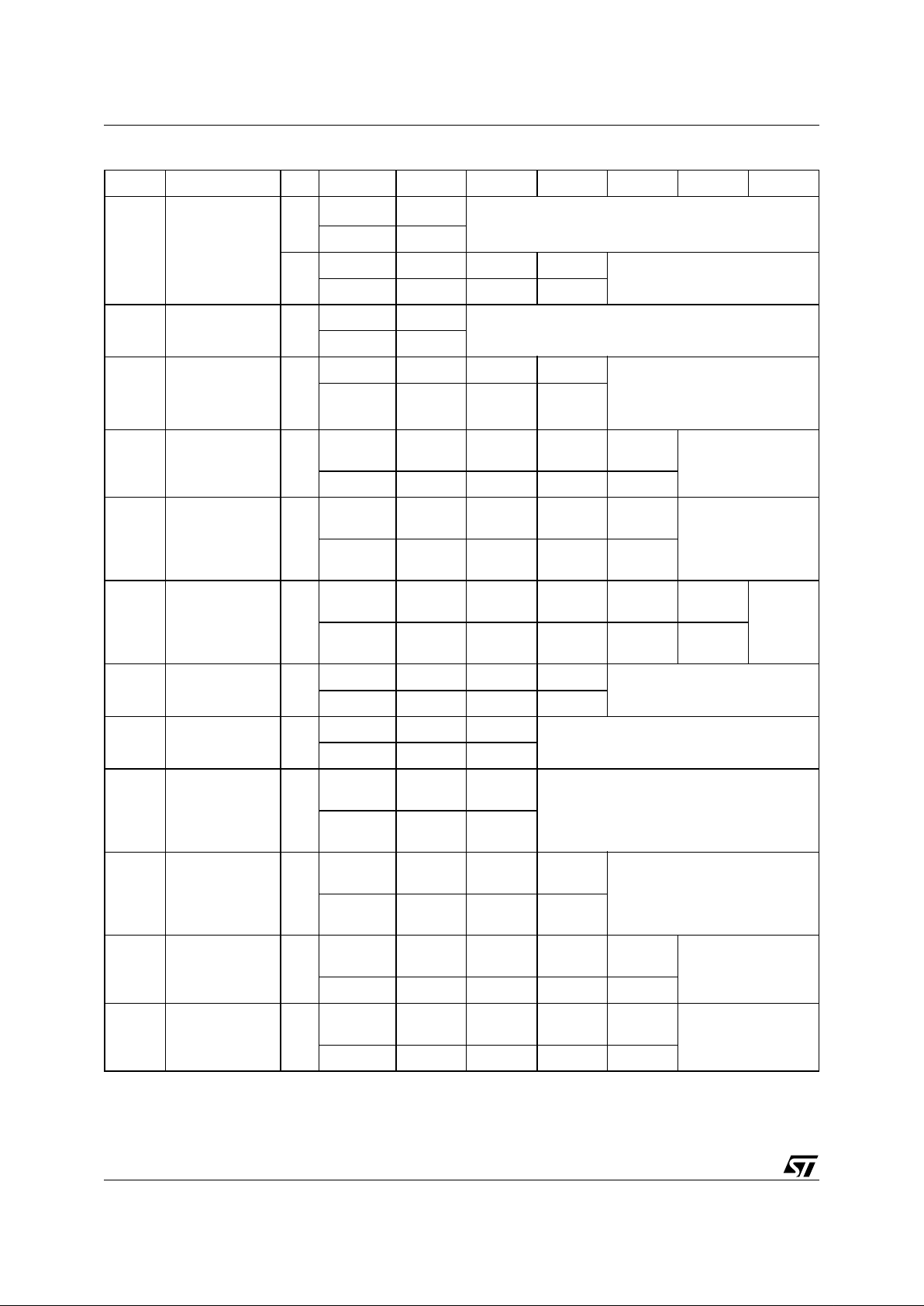
Table 14A. Instructions
(1,2)
Mne. Instr. Cyc. 1st Cyc. 2nd Cyc. 3rd Cyc. 4th Cyc. 5th Cyc. 6th Cyc.
RD
(4)
Read/Reset
Memory Array
1+
Addr.
(3)
X
Read Memory Array until a new write cycle is initiated.
Data F0h
3+
Addr. 555h 2AAh 555h
Read Memory Array until a new
write cycle is initiated.
Data AAh 55h F0h
RCFI CFI Query 1+
Addr. 55h
Read CFI data until a new write cycle is initiated.
Data 98h
AS
(4)
Auto Select 3+
Addr. 555h 2AAh 555h Read electronic Signature or
Block Protection or Configuration
Register Status until a new cycle
is initiated.
Data AAh 55h 90h
CR
Configuration
Register Write
4
Addr. 555h 2AAh 5 55h
Configuration Data
Data AAh 55h 60h 03h
PG Program 4
Addr. 555h 2AAh 555h
Program
Address
Read Data Polling or
Toggle Bit until
Program completes.
Data AAh 55h A0h
Program
Data
DPG
Double Word
Program
5
Addr. 555h 2AAh 5 55h
Program
Address 1
Program
Address 2
Note 6, 7
Data AAh 55h 40h
Program
Data 1
Program
Data 2
EBY
Enter Bypass
Mode
3
Addr. 555h 2AAh 555h
Data AAh 55h 20h
XBY
Exit Bypass
Mode
2
Addr. XX
Data 90h 00h
PGBY
Program in
Bypass Mode
2
Addr. X
Program
Address
Read Data Polling or Toggle Bit until Program
completes.
Data A0h
Program
Data
DPGBY
Double Word
Program in
Bypass Mode
3
Addr. X
Program
Address 1
Program
Address 2
Note 6, 7
Data 40h
Program
Data 1
Program
Data 2
BP Block Protect 4
Addr. 555h 2AAh 555h
Block
Address
Data AAh 55h 60h 01h
BU Block Unprotect 1
Addr. 555h 2AAh 555h
Block
Address
Data AAh 55h 60h D0h

13/38
M59DR032A, M59DR032B
Table 14B. Instructions
(1,2)
Note: 1. Commands not interpreted in this table will default to read array mode.
2. For Coded cycles address input s A 11-A20 are don’t care.
3. X = Don’t Care.
4. The fi rst cycles of the RD or AS inst ructions are followed by read operations. Any number of read cycles can occur after the command cycl e s.
5. During Erase Suspend, Read and Data Program functions are allow ed in blocks not bei ng erased.
6. Pr ogram Address 1 and Program Address 2 mus t be consecut i ve addresse s differing only for addre ss bit A0.
7. High voltage on V
PP
(11.4V to 12.6V) is required for th e proper execution of t he Double Wo rd P rogram instruction .
Mne. Instr. Cyc. 1st Cyc. 2nd Cyc. 3rd Cyc. 4th Cyc. 5th Cyc. 6th Cyc.
BL Block Lock 4
Addr. 555h 2AAh 555h
Block
Address
Data AAh 55h 60h 2Fh
BE Block Erase 6+
Addr. 555h 2AAh 555h 555h 2AAh
Block
Address
Data AAh 55h 80h AAh 55h 30h
BKE Bank Erase 6
Addr. 555h 2AAh 555h 555h 2AAh
Bank
Address
Data AAh 55h 80h AAh 55h 10h
ES Erase Suspend 1
Addr.
(3)
X
Read until Toggle stops, then read all the data needed
from any Blocks not being erased then Resume Erase.
Data B0h
ER Erase Resume 1
Addr.
Bank
Address
Read Data Polling or Toggle Bits until Erase completes or
Erase is suspended another time
Data 30h

M59DR032A, M59DR032B
14/38
Table 15. Query Structure Overvi ew
Note: The Flash memory d i splay the CFI data structure when CFI Query comm and is iss ued. In thi s table are listed the main su b-sections
detailled in Tables 16, 17 and 18. Query data are always presented on the lowest order data outputs.
Table 16. CFI Query Identification String
Note: Query data are always presented on the lowest - or der data outputs (DQ7-D Q0) only. DQ8-DQ15 are ‘0’ .
Offset Sub-section Name Description
00h Reserved Reserved for algorithm-specific information
10h CFI Query Identification String Command set ID and algorithm data offset
1Bh System Interface Information Device timing & voltage information
27h Device Geometry Definition Flash device layout
P Primary Algorithm-specific Extended Query table
Additional information specific to the Primary
Algorithm (optional)
A Alternate Algorithm-specific Extended Query table
Additional information specific to the Alternate
Algorithm (optional)
Offset Data Description
00h 0020h Manufacturer Code
01h
00A1h - bottom
00A0h - top
Device Code
02h-0Fh reserved Reserved
10h 0051h Query Unique ASCII String "QRY"
11h 0052h Query Unique ASCII String "QRY"
12h 0059h Query Unique ASCII String "QRY"
13h 0002h
Primary Algorithm Command Set and Control Interface ID code 16 bit ID code
defining a specific algorithm
14h 0000h
15h offset = P = 0040h
Address for Primary Algorithm extended Query table
16h 0000h
17h 0000h
Alternate V endor Command Set and Control Interface ID Code second vendor
- specified algorithm supported (note: 0000h means none exists)
18h 0000h
19h value = A = 0000h
Address for Alternate Algorithm extended Query table
note: 0000h means none exists
1Ah 0000h

15/38
M59DR032A, M59DR032B
Table 17. CFI Query System Interface Information
Offset Data Description
1Bh 0017h
V
DD
Logic Supply Minimum Program/Erase or Write voltage
bit 7 to 4 BCD value in volts
bit 3 to 0 BCD value in 100 millivolts
1Ch 0022h
V
DD
Logic Supply Maximum Program/Erase or Write voltage
bit 7 to 4 BCD value in volts
bit 3 to 0 BCD value in 100 millivolts
1Dh 0000h
V
PP
[Programming] Supply Minimum Program/Erase voltage
bit 7 to 4 HEX value in volts
bit 3 to 0 BCD value in 100 millivolts
Note: This value must be 0000h if no V
PP
pin is present
1Eh 00C0h
V
PP
[Programming] Supply Maximum Program/Erase voltage
bit 7 to 4 HEX value in volts
bit 3 to 0 BCD value in 100 millivolts
Note: This value must be 0000h if no V
PP
pin is present
1Fh 0004h
Typical timeout per single byte/word program (multi-byte program count = 1), 2
n
µs
(if supported; 0000h = not supported)
20h 0000h
Typical timeout for maximum-size multi-byte program or page write, 2
n
µs
(if supported; 0000h = not supported)
21h 000Ah
Typical timeout per individual block erase, 2
n
ms
(if supported; 0000h = not supported)
22h 0000h
Typical timeout for full chip erase, 2
n
ms
(if supported; 0000h = not supported)
23h 0004h
Maximum timeout for byte/word program, 2
n
times typical (offset 1Fh)
(0000h = not supported)
24h 0000h
Maximum timeout for multi-byte program or page write, 2
n
times typical (offset 20h)
(0000h = not supported)
25h 0004h
Maximum timeout per individual block erase, 2
n
times typical (offset 21h)
(0000h = not supported)
26h 0000h
Maximum timeout for chip erase, 2
n
times typical (offset 22h)
(0000h = not supported)

M59DR032A, M59DR032B
16/38
Table 18. Device Geometry Definition
Offset Word
Mode
Data Description
27h 0016h
Device Size = 2
n
in number of bytes
28h 0001h
Flash Device Interface Code description: Asynchronous x16
29h 0000h
2Ah 0000h
Maximum number of bytes in multi-byte program or page = 2
n
2Bh 0000h
2Ch 0002h Number of Erase Block Regions within device
bit 7 to 0 = x = number of Erase Block Regions
Note:1. x = 0 means no erase blocking, i.e. the device erases at once in "bulk."
2. x specifies the number of regions within the device containing one or more contiguous Erase Blo cks of the same siz e. Fo r ex ampl e, a 12 8KB devi ce ( 1Mb)
having blocking of 16KB, 8KB, four 2KB, two 16KB, and one 64KB is considered
to have 5 Erase Block Regions. Even thoug h two regions both contain 16KB
blocks, the f act that they are not c ontiguous means the y are separate Erase
Block Regions.
3. By definition, symmetrically block devices have only one blocking region.
M59DR032A M59DR032A Erase Block Region Information
bit 31 to 16 = z, where the Erase Block(s) within this Region are (z) times 256 bytes in
size. The value z = 0 is used for 128 byte block size.
e.g. for 64KB block size, z = 0100h = 256 => 256 * 256 = 64K
bit 15 to 0 = y, where y+1 = Number of Erase Blocks of identical size within the Erase
Block Region:
e.g. y = D15-D0 = FFFFh => y+1 = 64K blocks [maximum number]
y = 0 means no blocking (# blocks = y+1 = "1 block")
Note: y = 0 value must be used with number of block regions of one as indicated
by (x) = 0
2Dh 003Eh
2Eh 0000h
2Fh 0000h
30h 0001h
31h 0007h
32h 0000h
33h 0020h
34h 0000h
M59DR032B M59DR032B
2Dh 0007h
2Eh 0000h
2Fh 0020h
30h 0000h
31h 003Eh
32h 0000h
33h 0000h
34h 0001h

17/38
M59DR032A, M59DR032B
Table 19. Status Register Bits
(1)
Note: 1. Logic level ’1’ is High, ’0’ is Low. -0-1-0 -0-0-1-1 -1-0- represent bit va l ue i n successi ve Read operations.
2. In case of double word program DQ7
refers to the last word input.
DQ Name Logic Level Definition Note
7
Data
Polling
’1’
Erase Complete or erase block
in Erase Suspend.
Indicates the P/E.C. status, check
during Program or Erase, and on
completion before checking bits DQ5
for Program or Erase Success.
’0’ Erase On-going
DQ
Program Complete or data of
non erase block during Erase
Suspend.
DQ
Program On-going
(2)
6 Toggle Bit
’-1-0-1-0-1-0-1-’ Erase or Program On-going Successive reads output
complementary data on DQ6 while
Programming or Erase operations are
on-going. DQ6 remains at constant
level when P/E.C. operations are
completed or Erase Suspend is
acknowledged.
DQ Program Complete
’-1-1-1-1-1-1-1-’
Erase Complete or Erase
Suspend on currently addressed
block
5 Error Bit
’1’ Program or Erase Error
This bit is set to ’1’ in the case of
Programming or Erase failure.
’0’ Program or Erase On-going
4 Reserved
3
Erase Time
Bit
’1’ Erase Timeout Period Expired
P/E.C. Erase operation has started.
Only possible command entry is Erase
Suspend (ES)
’0’ Erase Timeout Period On-going
An additional block to be erased in
parallel can be entered to the P/E.C:
2 Toggle Bit
’-1-0-1-0-1-0-1-’
Erase Suspend read in the
Erase Suspended Block.
Erase Error due to the currently
addressed block (when DQ5 =
’1’).
Indicates the erase status and allows
to identify the erased block.
1
Program on-going or Erase
Complete.
DQ
Erase Suspend read on non
Erase Suspend block.
1 Reserved
0 Reserved

M59DR032A, M59DR032B
18/38
STATUS REGISTER BITS
P/E.C. status is indicated during execution by Data
Polling on D Q7, detection of T oggle on DQ6 and
DQ2, or Error on DQ5 bits. Any read attempt within
the Bank being modi fied and during Program or
Erase command e xecution will automa tically output these five Status Register bits. The P/E.C. automatically sets bits DQ2, DQ5, DQ6 and DQ7.
Other bits (DQ0, DQ1 and DQ4) are reserved for
future use and should be mas ked (see Tables 19
and 20). Read attemps within the bank not being
modified w ill ou t p ut arr ay d ata.
Data Polling Bit (DQ7). When Program ming operations are in progress, this bit out puts the complement of the bit being programmed on DQ7. In
case of a double word program operation, the
complement is done on DQ7 of the last word written to the command interface, i.e. the data written
in the fi fth cycl e. During E rase op eration, it output s
a ’0’. After completion of the operation, DQ7 wi ll
output the bit last programmed or a ’1’ after erasing. Data Polling is valid and only effective during
P/E.C. operation, that is after the fourth W
pulse
for programming or after the sixth W
pulse for
erase. It must be performed at t he address being
programmed or at an address within the block being erased. See Figure 12 for the Data Polling
flowchart and Figure 10 for the Data Polling waveforms. DQ7 will also flag the Erase Suspend mode
by switching from ’0’ to ’1’ at the start of the Erase
Suspend. In order to monitor DQ7 in the Erase
Suspend mode an address within a block being
erased must be provided. For a Read Operation in
Suspend mode, DQ7 will output ’1’ i f the read is attempted on a block being erased and the data value on other blocks. During Program operation in
Erase Suspend Mode, DQ7 will have the same behaviour as in the normal program exec ution outside of the suspend mode.
Toggle Bit (DQ6). When Programming or Erasing operations are in progress, successive attempts to read DQ6 will output complementary
data. DQ6 will toggle following toggling of either G
,
or E
when G is at VIL. The operation is completed
when two successive reads yield the same output
data. The next read will output the bit last programmed or a ’1’ after erasing. The toggle bit DQ6
is valid only during P/E.C. op erations, that is after
the fourth W
pulse for programming or after the
sixth W
pulse for Erase. DQ6 will be set to ’1’ if a
Read operation is attempted on an Erase Suspend
block. When erase is suspended DQ6 will toggle
during programming operations in a block different
from the block in E rase Suspend. Either E
or G
toggling will cause DQ6 to toggle. See Figure 13
for Toggle Bit flowchart and Fi gure 11 for Toggle
Bit waveforms.
Toggle Bit (DQ2). This toggle bit, together with
DQ6, can be used to det ermine the d evice status
during the Erase operations. During Erase Suspend a read from a block being erased will cause
DQ2 to toggle. A read from a block not being
erased will output data. DQ2 will be set to ’1’ during
program operation and to ‘0’ in Erase operation.
After erase completion and if the error bit DQ5 is
set to '1', DQ2 will toggle if the faulty block is addressed.
Error Bit (DQ5). This bit is set to '1' by the P/E.C.
when there is a failure of programming or block
erase, that results in invalid data in the memory
block. In case of an error in block erase or program, the block in which the error occurred or to
which the programmed data belongs, must be discarded. Other Blocks may still be used. The error
bit resets after a Read/Reset (RD) instruction. In
case of success of Program or Erase, the error bit
will be set to '0'.
Erase Timer Bit (DQ3). This bit is set to ‘0’ by the
P/E.C. when the last block Erase command has
been entered to the Co mmand Interface and it is
awaiting the Erase start. When the erase timeout
period is finished, DQ3 returns to ‘1’, in the range
of 80µs to 120µs.
Table 20. P o ll in g and Toggle B its
Mode DQ7 D Q6 DQ2
Program DQ7
Toggle 1
Erase 0 Toggle N/A
Erase Suspend Read
(in Erase Suspend
block)
1 1 Toggle
Erase Suspend Read
(outside Erase Suspend
block)
DQ7 DQ6 DQ2
Erase Suspend Program DQ7
Toggle 1

19/38
M59DR032A, M59DR032B
POWE R SU PPLY
Power Down
The memory provides Reset/Power Down c ontrol
input RP
. The Power Down function can be activated only if the relevant Configuration Register bit
is set to ’1’. In this case, when the RP
signal is
pulled at V
SS
the supply current drops to typically
I
CC2
(see Table 22), the memory is deselected and
the outputs are in high impedance.If RP
is pulled
to V
SS
during a Program o r Erase operation, this
operation is aborted in t
PLQ7V
and the memory
content is no longer valid (see Reset/Power Down
input description).
Power Up
The memory Command Interface is reset on Power Up to Read Array. Either E
or W must be tied to
V
IH
during Power Up to allow m aximum security
and the possibility to write a command on the first
rising edge of W
.
Supply Rails
Normal precautions must be taken for supply voltage decoupling; each device in a system should
have the V
DD
rails decoupled with a 0.1µF capac-
itor close to the V
DD
, V
DDQ
and VSS pins. The PCB
trace widths should be sufficient to carry the required V
DD
program and erase currents.
Table 21. Program, Erase Times and Progr am, Erase End uran ce Cycl es
(T
A
= 0 to 70°C; VDD = V
DDQ
= 1.65V to 2.2V, VPP = VDD unless otherwise specified)
Note: 1. M ax values refer to the m a ximum time all owed by the int ernal algorithm before error bi t is set. Worst case condi tions pr ogram o r
erase shou l d perform significantl y better.
2. Excl udes the time needed to exe cute the sequence for program instruction.
Parameter
M59DR032
Unit
Min
Max
(1)
Typ
Typical after
100k W/E Cycles
Parameter Block (4 KWord) Erase (Preprogrammed) 2.5 0.15 0.4 sec
Main Block (32 KWord) Erase (Preprogrammed) 10 1 3 sec
Bank Erase (Preprogrammed, Bank A) 2 6 sec
Bank Erase (Preprogrammed, Bank B) 10 30 sec
Chip Program
(2)
20 25 sec
Chip Program (DPG, V
PP
= 12V)
(2)
10 sec
Word Program 200 10 10 µs
Program/Erase Cycles (per Block) 100,000 cycles

M59DR032A, M59DR032B
20/38
Table 22. DC Characteristics
(TA = 0 to 70°C or –40 to 85°C; V
DD
= V
DDQ
= 1.65V to 2.2V)
Note: 1. Sampled only, not 100% tested.
2. V
PP
may be conne ct ed to 12V pow er supply for a total of less than 100 hrs.
3. For sta ndard prog ram/erase operation V
PP
is don’t car e.
Symbol Parameter Test Condition Min Typ Max Unit
I
LI
Input Leakage Current
0V ≤ V
IN
≤ V
DD
±1 µA
I
LO
Output Leakage Current
0V ≤ V
OUT
≤ V
DD
±5 µA
I
CC1
Supply Current
(Read Mode)
E
= VIL, G = VIH, f = 6MHz
10 20 mA
I
CC2
Supply Current
(Power Down)
RP
= VSS ± 0.2V
210µA
I
CC3
Supply Current (Standby)
E
= VDD ± 0.2V
15 50 µA
I
CC4
(1)
Supply Current
(Program or Erase)
Word Program, Block Erase
in progress
10 20 mA
I
CC5
(1)
Supply Current
(Dual Bank)
Program/Erase in progress
in one Bank, Read in the
other Bank
20 40 mA
I
PP1
VPP Supply Current
(Program or Erase)
V
PP
= 12V ± 0.6V
510mA
I
PP2
VPP Supply Current
(Standby or Read)
V
PP
≤ V
CC
0.2 5 µA
V
PP
= 12V ± 0.6V
100 400 µA
V
IL
Input Low Voltage –0.5 0.4 V
V
IH
Input High Voltage
V
DDQ
–0.4 V
DDQ
+ 0.4
V
V
OL
Output Low Voltage
I
OL
= 100µA
0.1 V
V
OH
Output High Voltage
CMOS
I
OH
= –100µA V
DDQ
–0.1
V
V
PP
(2,3)
VPP Supply Voltage
(Program or Erase)
–0.4
V
DD
+ 0.4
V
Double Word Program 11.4 12.6 V

21/38
M59DR032A, M59DR032B
Table 23. Capacitance
(1)
(T
A
= 25 °C, f = 1 MHz)
Note: 1. Sampled only, not 100% tested.
Symbol Parameter Test Condition Min Max Unit
C
IN
Input Capacitance
V
IN
= 0V
6pF
C
OUT
Output Capacitance
V
OUT
= 0V
12 pF
Figure 4. AC Testing Load Circuit
AI02316
V
DDQ
/ 2
OUT
CL = 30pF
CL includes JIG capacitance
3.3kΩ
1N914
DEVICE
UNDER
TEST
Table 24. AC Measuremen t Cond itions
Input Rise and Fall Times
≤
4ns
Input Pulse Voltages
0 to V
DDQ
Input and Output Timing Ref. Voltages
V
DDQ
/2
Figure 3. Tes ting Inp ut/ Output Wav ef orms
AI02315
V
DDQ
0V
V
DDQ
/2

M59DR032A, M59DR032B
22/38
Table 25. Read AC Characteristics
(TA = 0 to 70°C or –40 to 85°C; V
DD
= V
DDQ
= 1.65V to 2.2V)
Note: 1. Sampled only, not 100% tested.
2. G
may be delayed by up to t
ELQV
- t
GLQV
after the fal ling edge of E without increasi ng t
ELQV
.
Symbol Alt Parameter Test Condition
M59DR032
Unit100 120
Min Max Min Max
t
AVAV
t
RC
Address Valid to Next
Address Valid
E
= VIL, G = V
IL
100 120 ns
t
AVQV
t
ACC
Address Valid to Output
Valid (Random)
E
= VIL, G = V
IL
100 120 ns
t
AVQV1
t
PAGE
Address Valid to Output
Valid (Page)
E
= VIL, G = V
IL
35 45 ns
t
ELQX
(1)
t
LZ
Chip Enable Low to Output
Transition
G
= V
IL
00ns
t
ELQV
(2)
t
CE
Chip Enable Low to Output
Valid
G
= V
IL
100 120 ns
t
GLQX
(1)
t
OLZ
Output Enable Low to
Output Transition
E
= V
IL
00ns
t
GLQV
(2)
t
OE
Output Enable Low to
Output Valid
E
= V
IL
25 35 ns
t
EHQX
t
OH
Chip Enable High to Output
T ransition
G
= V
IL
00ns
t
EHQZ
(1)
t
HZ
Chip Enable High to Output
Hi-Z
G
= V
IL
25 35 ns
t
GHQX
t
OH
Output Enable High to
Output Transition
E
= V
IL
00ns
t
GHQZ
(1)
t
DF
Output Enable High to
Output Hi-Z
E
= V
IL
25 35 ns
t
AXQX
t
OH
Address Transition to
Output Transition
E
= VIL, G = V
IL
00ns
t
PHQ7V1
RP High to Data Valid
(Read Mode)
150 150 ns
t
PHQ7V2
RP High to Data Valid
(Power Down enabled)
50 50 µs
t
PLQ7V
RP Low to Reset Complete
During Program/Erase
15 µs
t
PLPH
t
RP
RP Pulse Width 100 100 ns

23/38
M59DR032A, M59DR032B
Figure 5. Random Read AC Waveforms
AI02624
tAVAV
tAVQV tAXQX
tELQX tEHQX
tGLQV
tGLQX
tGHQX
VALID
A0-A20
E
G
DQ0-DQ15
tELQV
VALID
tEHQZ
tGHQZ
Note: Wri te Enable (W) = High.

M59DR032A, M59DR032B
24/38
Figure 6. Page R ea d AC Wa v e form s
AI02538
E
G
DQ0-DQ15
A2-A20
VALID
A0-A1
VALID
VALID
tEHQX
tGHQZ
tGHQX
tEHQZ
tELQV
tGLQV
tAVQV
VALIDVALID
VALID
VALID VALID VALID
tAVQV1

25/38
M59DR032A, M59DR032B
Table 26. Write AC Characteristics, Write Enable Controlled
(T
A
= 0 to 70 °C or –40 to 85 °C; VDD = V
DDQ
= 1.65V to 2.2V)
Symbol Alt Parameter
M59DR032
Unit100 120
Min Max Min Max
t
AVAV
t
WC
Address Valid to Next Address Valid 100 120 ns
t
ELWL
t
CS
Chip Enable Low to Write Enable Low 0 0 ns
t
WLWH
t
WP
Write Enable Low to Write Enable High 50 50 ns
t
DVWH
t
DS
Input Valid to Write Enable High 50 50 ns
t
WHDX
t
DH
Write Enable High to Input Transition 0 0 ns
t
WHEH
t
CH
Write Enable High to Chip Enable High 0 0 ns
t
WHWL
t
WPH
Write Enable High to Write Enable Low 30 30 ns
t
AVWL
t
AS
Address Valid to Write Enable Low 0 0 ns
t
WLAX
t
AH
Write Enable Low to Address Transition 50 50 ns
t
GHWL
Output Enable High to Write Enable Low 0 0 ns
t
VDHEL
t
VCSVDD
High to Chip Enable Low
50 50 µs
t
WHGL
t
OEH
Write Enable High to Output Enable Low 30 30 ns
t
PLQ7V
RP Low to Reset Complete During
Program/Erase
15 15 µs

M59DR032A, M59DR032B
26/38
Table 27. Write AC Characteristics, Chip Enable Controlled
(T
A
= 0 to 70 °C or –40 to 85 °C; VDD = V
DDQ
= 1.65V to 2.2V)
Symbol Alt Parameter
M59DR032
Unit100 120
Min Max Min Max
t
AVAV
t
WC
Address Valid to Next Address Valid 100 120 ns
t
WLEL
t
WS
Write Enable Low to Chip Enable Low 0 0 ns
t
ELEH
t
CP
Chip Enable Low to Chip Enable High 50 50 ns
t
DVEH
t
DS
Input Valid to Chip Enable High 50 50 ns
t
EHDX
t
DH
Chip Enable High to Input Transition 0 0 ns
t
EHWH
t
WH
Chip Enable High to Write Enable High 0 0 ns
t
EHEL
t
CPH
Chip Enable High to Chip Enable Low 30 30 ns
t
AVEL
t
AS
Address Valid to Chip Enable Low 0 0 ns
t
ELAX
t
AH
Chip Enable Low to Address Transition 50 50 ns
t
GHEL
Output Enable High Chip Enable Low 0 0 ns
t
VDHWL
t
VCSVDD
High to Write Enable Low
50 50 µs
t
EHGL
t
OEH
Chip Enable High to Output Enable Low 30 30 ns
t
PLQ7V
RP Low to Reset Complete During
Program/Erase
15 15 µs

27/38
M59DR032A, M59DR032B
Figure 7. Write AC Waveforms, W Controlled
Note: Address are latched on the falling edge of W, Dat a i s latched on the ri sing edge of W.
AI02539
E
G
W
A0-A20
DQ0-DQ15
VALID
VALID
V
DD
tVDHEL
tWHEH
tWHWL
tELWL
tAVWL
tWHGL
tWLAX
tWHDX
tAVAV
tDVWH
tWLWHtGHWL

M59DR032A, M59DR032B
28/38
Figure 8. Write AC Waveforms, E Controlled
Note: Address are latched on the falling edge of E, Dat a is latched on the risin g edge of E.
AI02540
E
G
W
A0-A20
DQ0-DQ15
VALID
VALID
V
DD
tVDHWL
tEHWH
tEHEL
tWLEL
tAVEL
tEHGL
tELAX
tEHDX
tAVAV
tDVEH
tELEHtGHEL

29/38
M59DR032A, M59DR032B
Table 28. Data Polling and Toggle Bits AC Characteristics
(1)
(TA = 0 to 70 °C or –40 to 85 °C; VDD = V
DDQ
= 1.65V to 2.2V)
Note: 1. All other timings are defined in Read AC Characteristics table.
Symbol Parameter
M59DR032
Unit
Min Max
t
WHQ7V
Write Enable High to DQ7 Valid (Program, W Controlled) 10 200 µs
Write Enable High to DQ7 Valid (Block Erase, W
Controlled) 1.0 10 sec
t
EHQ7V
Chip Enable High to DQ7 Valid (Program, E Controlled) 10 200 µs
Chip Enable High to DQ7 Valid (Block Erase, E
Controlled) 1.0 10 sec
t
Q7VQV
Q7 Valid to Output Valid (Data Polling) 0 ns
t
WHQV
Write Enable High to Output Valid (Program) 10 200 µs
Write Enable High to Output Valid (Block Erase) 1.0 10 sec
t
EHQV
Chip Enable High to Output Valid (Program) 10 200 µs
Chip Enable High to Output Valid (Block Erase) 1.0 10 sec

M59DR032A, M59DR032B
30/38
Figure 9. Read and Write AC Characteristics, RP Related
AI02619
DQ7
W
RP
tPLPH
tPHQ7V
VALID
READ
DQ7 VALID
tPLQ7V
PROGRAM / ERASE

31/38
M59DR032A, M59DR032B
Figure 10. Data Polling DQ7 AC Waveforms
AI02625
E
G
W
A0-A20
DQ7
IGNORE
VALID
DQ0-DQ6/
DQ8-DQ15
ADDRESS (WITHIN BLOCKS)
tAVQV
tEHQ7V
tGLQV
tWHQ7V
VALID
tQ7VQV
DQ7
DATA POLLING (LAST) CYCLE MEMORY
ARRAY
READ CYCLE
DATA POLLING
READ CYCLES
LAST WRITE
CYCLE OF
PROGRAM
OR ERASE
INSTRUCTION
tELQV

M59DR032A, M59DR032B
32/38
Figure 11. Data Toggle DQ6, DQ2 AC Waveforms
AI02543
E
G
W
A0-A20
DQ6,DQ2
tAVQV
STOP TOGGLE
LAST WRITE
CYCLE OF
PROGRAM
OF ERASE
INSTRUCTION
VALID
VALID
VALID
IGNORE
DATA TOGGLE
READ CYCLE
MEMORY ARRAY
READ CYCLE
tWHQV
tEHQV
tELQV
tGLQV
DATA
TOGGLE
READ CYCLE
DQ0-DQ1,DQ3-DQ5,
DQ7-DQ15
Note: All other timings are as a norm a l Read cycle.

33/38
M59DR032A, M59DR032B
Figure 12. Data Polling Flowchart
READ DQ5 & DQ7
at VALID ADDRESS
START
READ DQ7
FAIL PASS
AI02574
DQ7
=
DATA
YES
NO
YES
NO
DQ5
= 1
DQ7
=
DATA
YES
NO
Figure 13. Data Toggle Flowchart
READ
DQ5 & DQ6
START
READ DQ6
FAIL PASS
AI02626
DQ6
=
TOGGLES
NO
NO
YES
YES
DQ5
= 1
NO
YES
DQ6
=
TOGGLES

M59DR032A, M59DR032B
34/38
Table 29. Ordering Information Scheme
Devices are shipped from the factory with the memory content erased (to FFFFh).
For a list of available options (Speed, Pac kage, etc...) or for furthe r information on any aspect of this device, please contact the STMicroelectronics Sales Office nearest to you.
Table 30. Revision History
Example: M59DR032A 100 ZB 6 T
Device Type
M59
Architecture
D = Dual Bank Page Mode
Operating Voltage
R = 1.8V
Device Function
032A = 32 Mbit (2Mb x16), Dual Bank: 1/8-7/8 partitioning, Top Boot
032B = 32 Mbit (2Mb x16), Dual Bank: 1/8-7/8 partitioning, Bottom Boot
032C = 32 Mbit (2Mb x16), Dual Bank: 1/4-3/4 partitioning, Top Boot
032D = 32 Mbit (2Mb x16), Dual Bank: 1/4-3/4 partitioning, Bottom Boot
032E = 32 Mbit (2Mb x16), Dual Bank: 1/half-1/half partitioning, Top Boot
032F = 32 Mbit (2Mb x16), Dual Bank: 1/half-1/half partitioning, Bottom Boot
Random Speed
100 = 100 ns
120 = 120 ns
Package
N = TSOP48: 12 x 20mm
ZB = FBGA48: 0.75mm pitch
Temperature Range
1 = 0 to 70°C
6 = –40 to 85°C
Option
T = Tape & Reel packing
Date Revision Details
May 1999 First Issue
09/03/99
FBGA Package Outline drawing change
FBGA Connections change (Table 1, Figure 2A)
t
WHGL
and t
EHGL
Specification change (Table 26, 27)
10/20/99 Daisy Chain diagrams, Package and PCB Connections, added (Figure 16, 17)

35/38
M59DR032A, M59DR032B
Table 31. TSOP48 - 48 lead Plastic Thin Small Outline, 12 x 20 mm, Package Mechanical Data
Symbol
mm inches
Typ Min Max Typ Min Max
A 1.20 0.047
A1 0.05 0.15 0.002 0.006
A2 0.95 1.05 0.037 0.041
B 0.17 0.27 0.007 0.011
C 0.10 0.21 0.004 0.008
D 19.80 20.20 0.780 0.795
D1 18.30 18.50 0.720 0.728
E 11.90 12.10 0.469 0.476
e 0.50 – – 0.020 – –
L 0.50 0.70 0.020 0.028
α
0° 5° 0° 5°
N48 48
CP 0.10 0.004
Figure 14. TSOP48 - 48 lead Plastic Thin Small Outline, 12 x 20 mm, Package Outline
Drawing is not to scale.
TSOP-a
D1
E
1 N
CP
B
e
A2
A
N/2
D
DIE
C
LA1 α

M59DR032A, M59DR032B
36/38
Table 32. FBGA48 - 8 x 6 balls, 0.75 mm pitch, Package Mechanical Data
Symbol
mm inches
Typ Min Max Typ Min Max
A 1.250 0.492
A1 0.300 0.250 0.350 0.012 0.010 0.014
A2 0.700 0.275
b 0.450 0.400 0.550 0.018 0.016 0.022
ddd 0.075 0.003
D 7.000 6.800 7.200 0.276 0.268 0.283
D1 5.250 – – 0.207 – –
e 0.750 – – 0.030 – –
E 12.000 11.800 12.200 0.472 0.465 0.480
E1 3.750 – – 0.148 – –
SD 0.375 – – 0.015 – –
SE 0.375 – – 0.015 – –
Figure 15. FBGA48 - 8 x 6 balls, 0.75 mm pitch, Package Outline
Drawing is not to scale.
E1E
D1
D
A2
A1
A
BGA-Z03
ddd
BALL "A1"
eb
SD
SE

37/38
M59DR032A, M59DR032B
Figure 16. Daisy Chain - Package Connections (Top View)
Figure 17. Daisy Chain - PCB Connections (Top View)
AI03079
C
B
A
87654321
E
D
F
AI3080
C
B
A
87654321
E
D
F
START
STOP

M59DR032A, M59DR032B
38/38
Information furnished is believed to be ac curate and reli able. Howev er, STMicroel ectronics assumes no responsibilit y for the consequence s
of use of such information nor for any infringement of patents or other rights of third parties which may result from its use. No license is granted
by implic ation or otherwise under any patent or patent rights of STMi croelectr onics. Specifications mentioned in thi s publicati on are subject
to change without notice. This publication supersedes and replaces all information previously supplied. STMicroelectronics products are not
authorized for use as cri tical comp onents in life support dev i ces or systems wi t hout express written ap proval of STMi croelect ro nics.
The ST log o i s registered trademark of STMicroelectronics
1999 STMi croelectr oni cs - All Rights Reserved
All other names are the property of their respective owners.
STMicroelect ro n ics GRO UP OF COMPANI ES
Australi a - Brazil - Chi na - Finland - F rance - Germ any - Hong K ong - India - Ita l y - Japan - Mala ysia - Malta - Moroc co -
Singapor e - Spain - Sweden - Switzerl and - United Kingdom - U .S .A.
http://www.st.com
 Loading...