

ST M48Z58, M48Z58Y User Manual
M48Z58
M48Z58Y
5 V, 64 Kbit (8 Kbit x 8) ZEROPOWER® SRAM
Features
■ Integrated, ultra low power SRAM, power-fail
control circuit, and battery
■ READ cycle time equals WRITE cycle time
■ Automatic power-fail chip deselect and WRITE
protection
■ WRITE protect voltages:
(V
= power-fail deselect voltage)
PFD
–M48Z58: V
4.5 V ≤ V
–M48Z58Y: V
4.2 V ≤ V
■ Self-contained battery in the CAPHAT
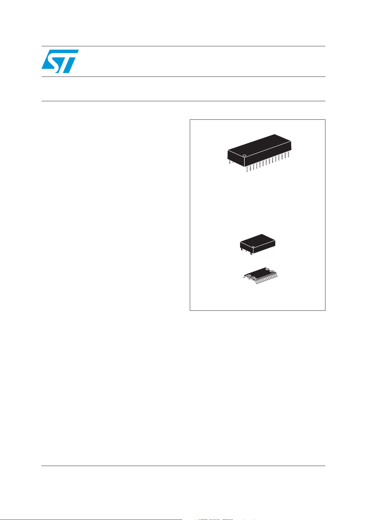
package
■ Packaging includes a 28-lead SOIC and
SNAPHAT
■ SOIC package provides direct connection for a
SNAPHAT
■ Pin and function compatible with JEDEC
standard 8 Kbit x 8 SRAMs
■ RoHS compliant
– Lead-free second level interconnect
= 4.75 to 5.5 V;
CC
≤ 4.75 V
PFD
= 4.5 to 5.5 V;
CC
≤ 4.5 V
PFD
®
top (to be ordered separately)
®
top which contains the battery
™
DIP
28
1
PCDIP28
battery CAPHAT™
®
battery
1
SOH28
2
8
SNAPHAT
June 2011 Doc ID 2559 Rev 11 1/24
www.st.com
1

Contents M48Z58, M48Z58Y
Contents
1 Description . . . . . . . . . . . . . . . . . . . . . . . . . . . . . . . . . . . . . . . . . . . . . . . . . 5
2 Operating modes . . . . . . . . . . . . . . . . . . . . . . . . . . . . . . . . . . . . . . . . . . . . 8
2.1 READ mode . . . . . . . . . . . . . . . . . . . . . . . . . . . . . . . . . . . . . . . . . . . . . . . . 8
2.2 WRITE mode . . . . . . . . . . . . . . . . . . . . . . . . . . . . . . . . . . . . . . . . . . . . . . . 9
2.3 Data retention mode . . . . . . . . . . . . . . . . . . . . . . . . . . . . . . . . . . . . . . . . . 11
2.4 V
noise and negative going transients . . . . . . . . . . . . . . . . . . . . . . . . . 12
CC
3 Maximum ratings . . . . . . . . . . . . . . . . . . . . . . . . . . . . . . . . . . . . . . . . . . . 13
4 DC and AC parameters . . . . . . . . . . . . . . . . . . . . . . . . . . . . . . . . . . . . . . 14
5 Package mechanical data . . . . . . . . . . . . . . . . . . . . . . . . . . . . . . . . . . . . 17
6 Part numbering . . . . . . . . . . . . . . . . . . . . . . . . . . . . . . . . . . . . . . . . . . . . 21
7 Environmental information . . . . . . . . . . . . . . . . . . . . . . . . . . . . . . . . . . . 22
8 Revision history . . . . . . . . . . . . . . . . . . . . . . . . . . . . . . . . . . . . . . . . . . . 23
2/24 Doc ID 2559 Rev 11

M48Z58, M48Z58Y List of tables
List of tables
Table 1. Signal names . . . . . . . . . . . . . . . . . . . . . . . . . . . . . . . . . . . . . . . . . . . . . . . . . . . . . . . . . . . . 6
Table 2. Operating modes . . . . . . . . . . . . . . . . . . . . . . . . . . . . . . . . . . . . . . . . . . . . . . . . . . . . . . . . . 8
Table 3. READ mode AC characteristics . . . . . . . . . . . . . . . . . . . . . . . . . . . . . . . . . . . . . . . . . . . . . . 9
Table 4. WRITE mode AC characteristics . . . . . . . . . . . . . . . . . . . . . . . . . . . . . . . . . . . . . . . . . . . . 11
Table 5. Absolute maximum ratings . . . . . . . . . . . . . . . . . . . . . . . . . . . . . . . . . . . . . . . . . . . . . . . . . 13
Table 6. Operating and AC measurement conditions . . . . . . . . . . . . . . . . . . . . . . . . . . . . . . . . . . . . 14
Table 7. Capacitance . . . . . . . . . . . . . . . . . . . . . . . . . . . . . . . . . . . . . . . . . . . . . . . . . . . . . . . . . . . . 14
Table 8. DC characteristics. . . . . . . . . . . . . . . . . . . . . . . . . . . . . . . . . . . . . . . . . . . . . . . . . . . . . . . . 15
Table 9. Power down/up AC characteristics . . . . . . . . . . . . . . . . . . . . . . . . . . . . . . . . . . . . . . . . . . . 16
Table 10. Power down/up trip points DC characteristics . . . . . . . . . . . . . . . . . . . . . . . . . . . . . . . . . . 16
Table 11. PCDIP28 – 28-pin plastic DIP, battery CAPHAT™, pack. mech. data . . . . . . . . . . . . . . . . 17
Table 12. SOH28 – 28-lead plastic small outline, battery SNAPHAT
Table 13. SH – 4-pin SNAPHAT
Table 14. SH – 4-pin SNAPHAT
Table 15. Ordering information scheme . . . . . . . . . . . . . . . . . . . . . . . . . . . . . . . . . . . . . . . . . . . . . . . 21
Table 16. SNAPHAT
®
battery table . . . . . . . . . . . . . . . . . . . . . . . . . . . . . . . . . . . . . . . . . . . . . . . . . . 21
®
housing for 48 mAh battery, package mech. data . . . . . . . . . . . . 19
®
housing for 120 mAh battery, pack. mech. data . . . . . . . . . . . . . . 20
Table 17. Document revision history . . . . . . . . . . . . . . . . . . . . . . . . . . . . . . . . . . . . . . . . . . . . . . . . . 23
®
, pack. mech. data . . . . . . . . . 18
Doc ID 2559 Rev 11 3/24

List of figures M48Z58, M48Z58Y
List of figures
Figure 1. Logic diagram . . . . . . . . . . . . . . . . . . . . . . . . . . . . . . . . . . . . . . . . . . . . . . . . . . . . . . . . . . . . 5
Figure 2. DIP connections . . . . . . . . . . . . . . . . . . . . . . . . . . . . . . . . . . . . . . . . . . . . . . . . . . . . . . . . . . 6
Figure 3. SOIC connections . . . . . . . . . . . . . . . . . . . . . . . . . . . . . . . . . . . . . . . . . . . . . . . . . . . . . . . . . 6
Figure 4. Block diagram . . . . . . . . . . . . . . . . . . . . . . . . . . . . . . . . . . . . . . . . . . . . . . . . . . . . . . . . . . . . 7
Figure 5. READ mode AC waveforms . . . . . . . . . . . . . . . . . . . . . . . . . . . . . . . . . . . . . . . . . . . . . . . . . 9
Figure 6. WRITE enable controlled, WRITE mode AC waveforms . . . . . . . . . . . . . . . . . . . . . . . . . . 10
Figure 7. Chip enable controlled, WRITE mode AC waveforms . . . . . . . . . . . . . . . . . . . . . . . . . . . . 10
Figure 8. Supply voltage protection . . . . . . . . . . . . . . . . . . . . . . . . . . . . . . . . . . . . . . . . . . . . . . . . . . 12
Figure 9. AC measurement load circuit . . . . . . . . . . . . . . . . . . . . . . . . . . . . . . . . . . . . . . . . . . . . . . . 14
Figure 10. Power down/up mode AC waveforms. . . . . . . . . . . . . . . . . . . . . . . . . . . . . . . . . . . . . . . . . 15
Figure 11. PCDIP28 – 28-pin plastic DIP, battery CAPHAT™, package outline . . . . . . . . . . . . . . . . . 17
Figure 12. SOH28 – 28-lead plastic small outline, battery SNAPHAT
Figure 13. SH – 4-pin SNAPHAT
Figure 14. SH – 4-pin SNAPHAT
Figure 15. Recycling symbols . . . . . . . . . . . . . . . . . . . . . . . . . . . . . . . . . . . . . . . . . . . . . . . . . . . . . . . 22
®
housing for 48 mAh battery, package outline . . . . . . . . . . . . . . . . 19
®
housing for 120 mAh battery, package outline . . . . . . . . . . . . . . . 20
®
, pack. outline. . . . . . . . . . . . . 18
4/24 Doc ID 2559 Rev 11
M48Z58, M48Z58Y Description
1 Description
The M48Z58/Y ZEROPOWER® RAM is an 8 Kbit x 8 non-volatile static RAM that integrates
power-fail deselect circuitry and battery control logic on a single die. The monolithic chip is
available in two special packages to provide a highly integrated battery-backed memory
solution.
The M48Z58/Y is a non-volatile pin and function equivalent to any JEDEC standard 8 K x 8
SRAM. It also easily fits into many ROM, EPROM, and EEPROM sockets, providing the
non-volatility of PROMs without any requirement for special WRITE timing or limitations on
the number of WRITEs that can be performed.
The 28-pin, 600 mil DIP CAPHAT
button cell in a single package.
™
houses the M48Z58/Y silicon with a long life lithium
The 28-pin, 330 mil SOIC provides sockets with gold plated contacts at both ends for direct
connection to a separate SNAPHAT
®
housing containing the battery. The unique design
allows the SNAPHAT battery package to be mounted on top of the SOIC package after the
completion of the surface mount process. Insertion of the SNAPHAT housing after reflow
prevents potential battery damage due to the high temperatures required for device surfacemounting. The SNAPHAT housing is keyed to prevent reverse insertion.
The SOIC and battery packages are shipped separately in plastic anti-static tubes or in tape
& reel form.
For the 28-lead SOIC, the battery package (e.g., SNAPHAT) part number is “M4Z28BR00SH1”.
Figure 1. Logic diagram
V
CC
A0-A12
W
13
M48Z58
M48Z58Y
E
8
DQ0-DQ7
G
V
SS
Doc ID 2559 Rev 11 5/24
AI01176B
Description M48Z58, M48Z58Y
Table 1. Signal names
A0-A12 Address inputs
DQ0-DQ7 Data inputs / outputs
E Chip enable input
G Output enable input
W WRITE enable input
V
CC
V
SS
NC Not connected internally
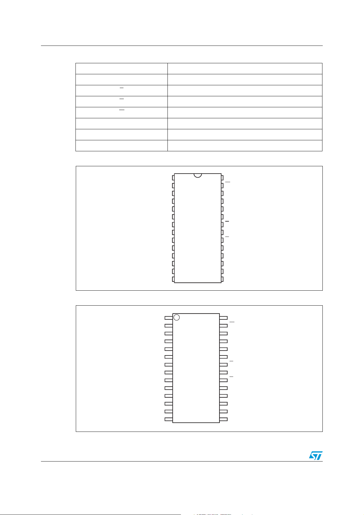
Figure 2. DIP connections
Supply voltage
Ground
NC V
1
A12
2
A7
3
A6
4
A5
5
A4
6
A3
7
8
9
10
11
M48Z58
M48Z58Y
A2
A1
A0
DQ0
12
DQ2
13
14
SS
28
27
26
25
24
23
22
21
20
19
18
17
16
15
CC
W
NC
A8
A9
A11
G
A10
E
DQ7
DQ6
DQ5DQ1
DQ4
DQ3V
AI01177B
Figure 3. SOIC connections
NC V
A12
A7
A6
A5
A4
A3
A2
A1
A0
DQ0
DQ2
SS
6/24 Doc ID 2559 Rev 11
1
2
3
4
5
6
7
8
9
10
11
12
13
14
M48Z58Y
28
27
26
25
24
23
22
21
20
19
18
17
16
15
CC
W
NC
A8
A9
A11
G
A10
E
DQ7
DQ6
DQ5DQ1
DQ4
DQ3V
AI01178B
M48Z58, M48Z58Y Description
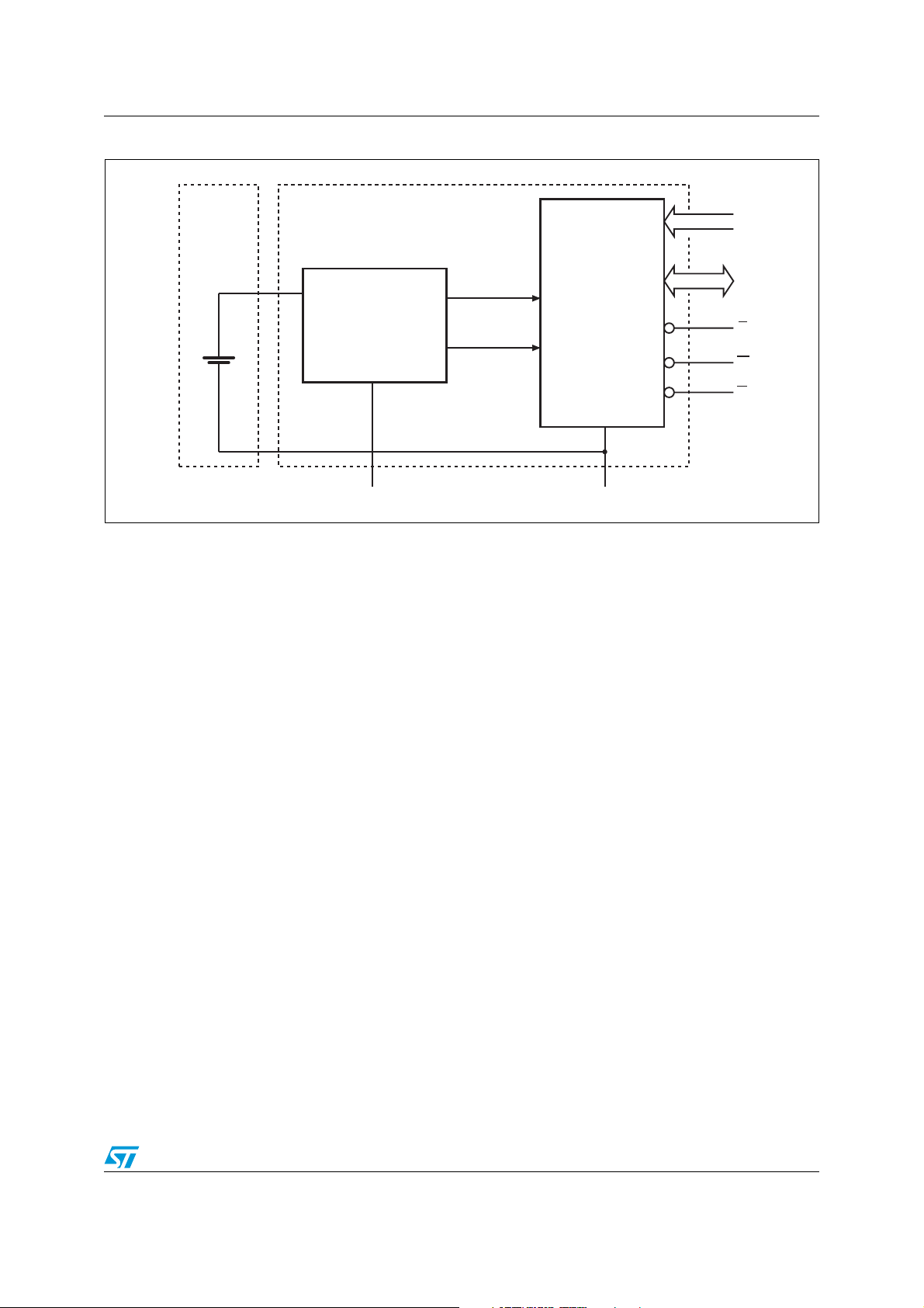
Figure 4. Block diagram
A0-A12
LITHIUM
CELL
VOLTAGE SENSE
AND
SWITCHING
CIRCUITRY
V
CC
POWER
V
PFD
8K x 8
SRAM ARRAY
V
SS
DQ0-DQ7
E
W
G
AI01394
Doc ID 2559 Rev 11 7/24
Operating modes M48Z58, M48Z58Y
2 Operating modes
The M48Z58/Y also has its own power-fail detect circuit. The control circuitry constantly
monitors the single 5 V supply for an out of tolerance condition. When V
tolerance, the circuit write protects the SRAM, providing a high degree of data security in the
midst of unpredictable system operation brought on by low V
switchover voltage (V
), the control circuitry connects the battery which maintains data
SO
. As VCC falls below battery
CC
until valid power returns.
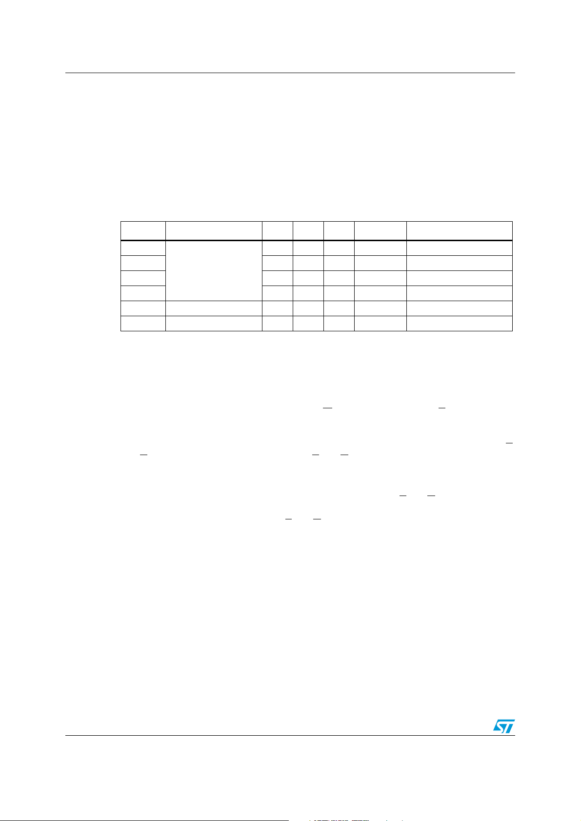
Table 2. Operating modes
Mode V
Deselect
WRITE V
READ V
READ V
Deselect V
Deselect ≤ V
1. See Table 10 on page 16 for details.
SO
CC
4.75 to 5.5 V
or
4.5 to 5.5 V
to V
PFD
SO
(min)
(1)
(1)
E G W DQ0-DQ7 Power
V
X X X High Z CMOS standby
X X X High Z Battery backup mode
X X High Z Standby
IH
XVILD
IL
V
IL
V
IL
V
IL
IH
IH
V
IH
IN
D
OUT
High Z Active
is out of
CC
Active
Active
Note: X = V
or VIL; VSO = Battery backup switchover voltage.
IH
2.1 READ mode
The M48Z58/Y is in the READ mode whenever W (WRITE enable) is high, E (chip enable) is
low. Thus, the unique address specified by the 13 address inputs defines which one of the
8,192 bytes of data is to be accessed. Valid data will be available at the data I/O pins within
address access time (t
and G
access times are also satisfied. If the E and G access times are not met, valid data
will be available after the latter of the chip enable access time (t
access time (t
The state of the eight three-state data I/O signals is controlled by E
activated before t
the address inputs are changed while E
for output data hold time (t
GLQV
) after the last address input signal is stable, providing that the E
AVQ V
) or output enable
ELQV
).
and G. If the outputs are
, the data lines will be driven to an indeterminate state until t
AVQ V
and G remain active, output data will remain valid
) but will go indeterminate until the next address access.
AXQX
AVQ V
. If
8/24 Doc ID 2559 Rev 11
 Loading...