

ST M48Z512A, M48Z512AY, M48Z512AV User Manual
M48Z512A
M48Z512AY, M48Z512AV
4 Mbit (512 Kbit x 8) ZEROPOWER® SRAM
Not recommended for new design
Features
■ Integrated, ultra low power SRAM, power-fail
control circuit, and battery
■ Conventional SRAM operation; unlimited
WRITE cycles
■ 10 years of data retention in the absence of
power
■ Automatic power-fail chip deselect and WRITE
protection
■ Two WRITE protect voltages:
(V
= power-fail deselect voltage)
PFD
–M48Z512A: V
4.5 V ≤ V
PFD
–M48Z512AY: V
4.2 V ≤ V
PFD
–M48Z512AV: V
2.8 V ≤ V
■ Battery internally isolated until power is applied
■ Pin and function compatible with JEDEC
PFD
standard 512 K x 8 SRAMs
■ PMDIP32 is an ECOPACK
■ RoHS compliant
– Lead-free second level interconnect
= 4.75 to 5.5 V;
CC
≤ 4.75 V
= 4.5 to 5.5 V;
CC
≤ 4.5 V
= 3.0 to 3.6 V;
CC
≤ 3.0 V
®
package
32
1
PMDIP32 module
Description
The M48Z512A/Y/V ZEROPOWER® RAM is a
non-volatile, 4,194,304-bit static RAM organized
as 524,288 words by 8 bits. The devices combine
an internal lithium battery, a CMOS SRAM and a
control circuit in a plastic, 32-pin DIP module.
June 2011 Doc ID 5146 Rev 9 1/21
This is information on a product still in production but not recommended for new designs.
www.st.com
1

Contents M48Z512A, M48Z512AY, M48Z512AV
Contents
1 Device overview . . . . . . . . . . . . . . . . . . . . . . . . . . . . . . . . . . . . . . . . . . . . 5
2 Operating modes . . . . . . . . . . . . . . . . . . . . . . . . . . . . . . . . . . . . . . . . . . . . 7
2.1 READ mode . . . . . . . . . . . . . . . . . . . . . . . . . . . . . . . . . . . . . . . . . . . . . . . . 7
2.2 WRITE mode . . . . . . . . . . . . . . . . . . . . . . . . . . . . . . . . . . . . . . . . . . . . . . . 9
2.3 Data retention mode . . . . . . . . . . . . . . . . . . . . . . . . . . . . . . . . . . . . . . . . . 11
2.4 V
noise and negative going transients . . . . . . . . . . . . . . . . . . . . . . . . . 12
CC
3 Maximum ratings . . . . . . . . . . . . . . . . . . . . . . . . . . . . . . . . . . . . . . . . . . . 13
4 DC and AC parameters . . . . . . . . . . . . . . . . . . . . . . . . . . . . . . . . . . . . . . 14
5 Package mechanical data . . . . . . . . . . . . . . . . . . . . . . . . . . . . . . . . . . . . 17
6 Part numbering . . . . . . . . . . . . . . . . . . . . . . . . . . . . . . . . . . . . . . . . . . . . 18
7 Environmental information . . . . . . . . . . . . . . . . . . . . . . . . . . . . . . . . . . . 19
8 Revision history . . . . . . . . . . . . . . . . . . . . . . . . . . . . . . . . . . . . . . . . . . . 20
2/21 Doc ID 5146 Rev 9

M48Z512A, M48Z512AY, M48Z512AV List of tables
List of tables
Table 1. Signal names . . . . . . . . . . . . . . . . . . . . . . . . . . . . . . . . . . . . . . . . . . . . . . . . . . . . . . . . . . . . 5
Table 2. Operating modes . . . . . . . . . . . . . . . . . . . . . . . . . . . . . . . . . . . . . . . . . . . . . . . . . . . . . . . . . 7
Table 3. READ mode AC characteristics . . . . . . . . . . . . . . . . . . . . . . . . . . . . . . . . . . . . . . . . . . . . . . 9
Table 4. WRITE mode AC characteristics . . . . . . . . . . . . . . . . . . . . . . . . . . . . . . . . . . . . . . . . . . . . 11
Table 5. Absolute maximum ratings . . . . . . . . . . . . . . . . . . . . . . . . . . . . . . . . . . . . . . . . . . . . . . . . . 13
Table 6. Operating and AC measurement conditions . . . . . . . . . . . . . . . . . . . . . . . . . . . . . . . . . . . . 14
Table 7. Capacitance . . . . . . . . . . . . . . . . . . . . . . . . . . . . . . . . . . . . . . . . . . . . . . . . . . . . . . . . . . . . 14
Table 8. DC characteristics. . . . . . . . . . . . . . . . . . . . . . . . . . . . . . . . . . . . . . . . . . . . . . . . . . . . . . . . 15
Table 9. Power down/up AC characteristics . . . . . . . . . . . . . . . . . . . . . . . . . . . . . . . . . . . . . . . . . . . 16
Table 10. Power down/up trip points DC characteristics . . . . . . . . . . . . . . . . . . . . . . . . . . . . . . . . . . 16
Table 11. PMDIP32 – 32-pin plastic DIP module, package mechanical data. . . . . . . . . . . . . . . . . . . 17
Table 12. Ordering information scheme . . . . . . . . . . . . . . . . . . . . . . . . . . . . . . . . . . . . . . . . . . . . . . . 18
Table 13. Revision history . . . . . . . . . . . . . . . . . . . . . . . . . . . . . . . . . . . . . . . . . . . . . . . . . . . . . . . . . 20
Doc ID 5146 Rev 9 3/21

List of figures M48Z512A, M48Z512AY, M48Z512AV
List of figures
Figure 1. Logic diagram . . . . . . . . . . . . . . . . . . . . . . . . . . . . . . . . . . . . . . . . . . . . . . . . . . . . . . . . . . . . 5
Figure 2. DIP connections . . . . . . . . . . . . . . . . . . . . . . . . . . . . . . . . . . . . . . . . . . . . . . . . . . . . . . . . . . 6
Figure 3. Block diagram . . . . . . . . . . . . . . . . . . . . . . . . . . . . . . . . . . . . . . . . . . . . . . . . . . . . . . . . . . . . 6
Figure 4. Chip enable or output enable controlled, READ mode AC waveforms. . . . . . . . . . . . . . . . . 8
Figure 5. Address controlled, READ mode AC waveforms . . . . . . . . . . . . . . . . . . . . . . . . . . . . . . . . . 8
Figure 6. WRITE enable controlled, WRITE AC waveforms . . . . . . . . . . . . . . . . . . . . . . . . . . . . . . . 10
Figure 7. Chip enable controlled, WRITE AC waveforms . . . . . . . . . . . . . . . . . . . . . . . . . . . . . . . . . 10
Figure 8. Supply voltage protection . . . . . . . . . . . . . . . . . . . . . . . . . . . . . . . . . . . . . . . . . . . . . . . . . . 12
Figure 9. AC measurement load circuit . . . . . . . . . . . . . . . . . . . . . . . . . . . . . . . . . . . . . . . . . . . . . . . 14
Figure 10. Power down/up mode AC waveforms. . . . . . . . . . . . . . . . . . . . . . . . . . . . . . . . . . . . . . . . . 15
Figure 11. PMDIP32 – 32-pin plastic DIP module, package outline . . . . . . . . . . . . . . . . . . . . . . . . . . 17
Figure 12. Recycling symbols . . . . . . . . . . . . . . . . . . . . . . . . . . . . . . . . . . . . . . . . . . . . . . . . . . . . . . . 19
4/21 Doc ID 5146 Rev 9
M48Z512A, M48Z512AY, M48Z512AV Device overview
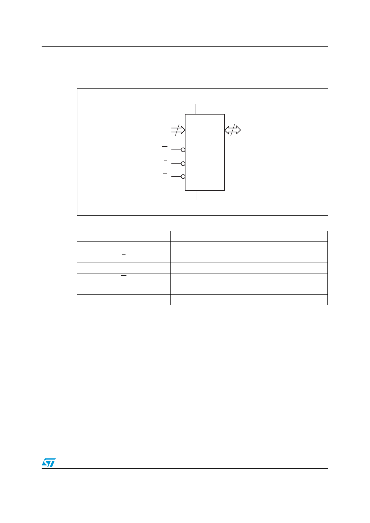
1 Device overview
Figure 1. Logic diagram
V
CC
Table 1. Signal names
A0-A18 Address inputs
DQ0-DQ7 Data inputs/outputs
E Chip enable input
G
W
V
CC
V
SS
A0-A18
W
19
M48Z512A
M48Z512AY
E
M48Z512AV
G
V
SS
Output enable input
WRITE enable input
Supply voltage
Ground
8
DQ0-DQ7
AI02043
Doc ID 5146 Rev 9 5/21

Device overview M48Z512A, M48Z512AY, M48Z512AV
Figure 2. DIP connections
A18 V
A16
A14
A12
A7
A6
A5
A4
A3
A2
A1
A0
DQ0
DQ2
SS
1
2
3
4
5
6
7
M48Z512A
8
M48Z512AY
9
M48Z512AV
10
11
12
13
14
15
16
32
31
30
29
28
27
26
25
24
23
22
21
20
19
18
17
CC
A15
A17
W
A13
A8
A9
A11
G
A10
E
DQ7
DQ6
DQ5DQ1
DQ4
DQ3V
AI02044
Figure 3. Block diagram
V
CC
POWER
VOLTAGE SENSE
E
AND
SWITCHING
CIRCUITRY
E
INTERNAL
BATTERY
512K x 8
SRAM ARRAY
V
SS
A0-A18
DQ0-DQ7
W
G
AI02045
6/21 Doc ID 5146 Rev 9
M48Z512A, M48Z512AY, M48Z512AV Operating modes
2 Operating modes
The M48Z512A/Y/V also has its own power-fail detect circuit. The control circuitry constantly
monitors the single V
tolerance, the circuit WRITE protects the SRAM, providing a high degree of data security in
the midst of unpredictable system operation brought on by low V
switchover voltage (V
until valid power returns.
The ZEROPOWER
PROMs without any requirement for special WRITE timing or limitations on the number of
WRITEs that can be performed.
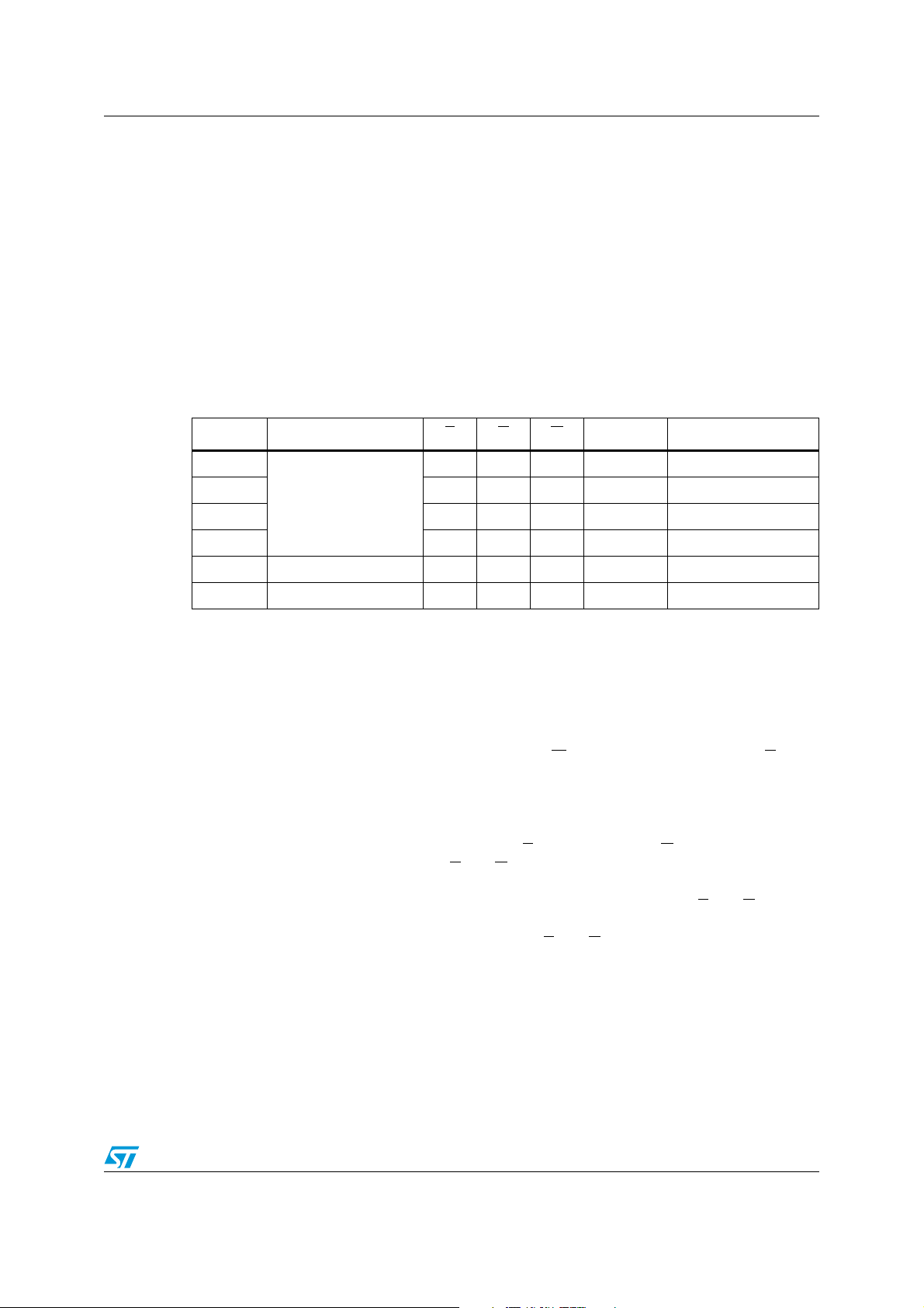
Table 2. Operating modes
supply for an out of tolerance condition. When VCC is out of
CC
. As VCC falls below the
), the control circuitry connects the battery which maintains data
SO
®
RAM replaces industry standard SRAMs. It provides the nonvolatility of
CC
Mode V
Deselect
WRITE V
READ V
READ V
Deselect V
Deselect ≤ V
1. X = VIH or VIL; VSO = battery backup switchover voltage.
SO
CC
4.75 to 5.5 V
or
4.5 to 5.5 V
or
3.0 to 3.6 V
to V
PFD
SO
(min)
(1)
(1)
Note: See Table 10 on page 16 for details.
2.1 READ mode
The M48Z512A/Y/V is in the READ mode whenever W (WRITE enable) is high and E (chip
enable) is low. The device architecture allows ripple-through access of data from eight of
4,194,304 locations in the static storage array. Thus, the unique address specified by the 19
address inputs defines which one of the 524,288 bytes of data is to be accessed. Valid data
will be available at the data I/O pins within address access time (t
address input signal is stable, providing that the E
access times are also satisfied. If the E
available after the later of chip enable access time (t
(t
). The state of the eight three-state data I/O signals is controlled by E and G. If the
GLQV
outputs are activated before t
until t
. If the address inputs are changed while E and G remain low, output data will
AVQ V
remain valid for output data hold time (t
access.
, the data lines will be driven to an indeterminate state
AVQ V
E G W DQ0-DQ7 Power
V
IH
IL
IL
IL
X X X High Z CMOS standby
X X X High Z Battery backup mode
X X High Z Standby
XVILD
V
V
V
IL
IH
IH
V
IH
IN
D
OUT
High Z Active
) after the last
AVQ V
Active
Active
(chip enable) and G (output enable)
and G access times are not met, valid data will be
) or output enable access Time
ELQV
) but will go indeterminate until the next address
AXQX
Doc ID 5146 Rev 9 7/21
 Loading...