

5 V or 3.3 V, 16 Mbit (2 Mb x 8) ZEROPOWER® SRAM
Features
■ Integrated, ultra low power SRAM, power-fail
control circuit, and batteries
■ Conventional SRAM operation; unlimited
WRITE cycles
■ 10 years of data retention in the absence of
power
■ Automatic power-fail chip deselect and WRITE
protection
■ WRITE protect voltages
(V
= power-fail deselect voltage):
PFD
–M48Z2M1Y: V
4.2 V ≤ V
PFD
–M48Z2M1V: V
2.8 V ≤ V
■ Batteries are internally isolated until power is
PFD
applied
■ Pin and function compatible with JEDEC
standard 2 Mb x 8 SRAMs
■ RoHS compliant
– Lead-free second level interconnect
= 4.5 to 5.5 V;
CC
≤ 4.5 V
= 3.0 to 3.6 V;
CC
≤ 3.0 V
M48Z2M1Y
M48Z2M1V
Not recommended for new design
36
1
PLDIP36 module
June 2011 Doc ID 5135 Rev 6 1/20
This is information on a product still in production but not recommended for new designs.
www.st.com
1

Contents M48Z2M1Y, M48Z2M1V
Contents
1 Description . . . . . . . . . . . . . . . . . . . . . . . . . . . . . . . . . . . . . . . . . . . . . . . . . 5
2 Operation modes . . . . . . . . . . . . . . . . . . . . . . . . . . . . . . . . . . . . . . . . . . . . 7
2.1 READ mode . . . . . . . . . . . . . . . . . . . . . . . . . . . . . . . . . . . . . . . . . . . . . . . . 7
2.2 WRITE mode . . . . . . . . . . . . . . . . . . . . . . . . . . . . . . . . . . . . . . . . . . . . . . . 9
2.3 Data retention mode . . . . . . . . . . . . . . . . . . . . . . . . . . . . . . . . . . . . . . . . . 10
2.4 V
noise and negative going transients . . . . . . . . . . . . . . . . . . . . . . . . . 11
CC
3 Maximum ratings . . . . . . . . . . . . . . . . . . . . . . . . . . . . . . . . . . . . . . . . . . . 12
4 DC and AC parameters . . . . . . . . . . . . . . . . . . . . . . . . . . . . . . . . . . . . . . 13
5 Package mechanical data . . . . . . . . . . . . . . . . . . . . . . . . . . . . . . . . . . . . 16
6 Part numbering . . . . . . . . . . . . . . . . . . . . . . . . . . . . . . . . . . . . . . . . . . . . 17
7 Environmental information . . . . . . . . . . . . . . . . . . . . . . . . . . . . . . . . . . . 18
8 Revision history . . . . . . . . . . . . . . . . . . . . . . . . . . . . . . . . . . . . . . . . . . . 19
2/20 Doc ID 5135 Rev 6

M48Z2M1Y, M48Z2M1V List of tables
List of tables
Table 1. Signal names . . . . . . . . . . . . . . . . . . . . . . . . . . . . . . . . . . . . . . . . . . . . . . . . . . . . . . . . . . . . 5
Table 2. Operating modes . . . . . . . . . . . . . . . . . . . . . . . . . . . . . . . . . . . . . . . . . . . . . . . . . . . . . . . . . 7
Table 3. READ mode AC characteristics . . . . . . . . . . . . . . . . . . . . . . . . . . . . . . . . . . . . . . . . . . . . . . 8
Table 4. WRITE mode AC characteristics . . . . . . . . . . . . . . . . . . . . . . . . . . . . . . . . . . . . . . . . . . . . 10
Table 5. Absolute maximum ratings . . . . . . . . . . . . . . . . . . . . . . . . . . . . . . . . . . . . . . . . . . . . . . . . . 12
Table 6. Operating and AC measurement conditions . . . . . . . . . . . . . . . . . . . . . . . . . . . . . . . . . . . . 13
Table 7. Capacitance . . . . . . . . . . . . . . . . . . . . . . . . . . . . . . . . . . . . . . . . . . . . . . . . . . . . . . . . . . . . 14
Table 8. DC characteristics. . . . . . . . . . . . . . . . . . . . . . . . . . . . . . . . . . . . . . . . . . . . . . . . . . . . . . . . 14
Table 9. Power down/up AC characteristics . . . . . . . . . . . . . . . . . . . . . . . . . . . . . . . . . . . . . . . . . . . 15
Table 10. Power down/up trip points DC characteristics . . . . . . . . . . . . . . . . . . . . . . . . . . . . . . . . . . 15
Table 11. PLDIP36 – 36-pin plastic DIP long module, package mechanical data . . . . . . . . . . . . . . . 16
Table 12. Ordering information scheme . . . . . . . . . . . . . . . . . . . . . . . . . . . . . . . . . . . . . . . . . . . . . . . 17
Table 13. Document revision history . . . . . . . . . . . . . . . . . . . . . . . . . . . . . . . . . . . . . . . . . . . . . . . . . 19
Doc ID 5135 Rev 6 3/20

List of figures M48Z2M1Y, M48Z2M1V
List of figures
Figure 1. Logic diagram . . . . . . . . . . . . . . . . . . . . . . . . . . . . . . . . . . . . . . . . . . . . . . . . . . . . . . . . . . . . 5
Figure 2. DIP connections . . . . . . . . . . . . . . . . . . . . . . . . . . . . . . . . . . . . . . . . . . . . . . . . . . . . . . . . . . 6
Figure 3. Block diagram . . . . . . . . . . . . . . . . . . . . . . . . . . . . . . . . . . . . . . . . . . . . . . . . . . . . . . . . . . . . 6
Figure 4. Address controlled, READ mode AC waveforms . . . . . . . . . . . . . . . . . . . . . . . . . . . . . . . . . 7
Figure 5. Chip enable or output enable controlled, READ mode AC waveforms. . . . . . . . . . . . . . . . . 8
Figure 6. WRITE enable controlled, WRITE mode AC waveforms . . . . . . . . . . . . . . . . . . . . . . . . . . . 9
Figure 7. Chip enable controlled, WRITE mode AC waveforms . . . . . . . . . . . . . . . . . . . . . . . . . . . . . 9
Figure 8. Supply voltage protection . . . . . . . . . . . . . . . . . . . . . . . . . . . . . . . . . . . . . . . . . . . . . . . . . . 11
Figure 9. AC testing load circuit . . . . . . . . . . . . . . . . . . . . . . . . . . . . . . . . . . . . . . . . . . . . . . . . . . . . . 13
Figure 10. Power down/up mode AC waveforms. . . . . . . . . . . . . . . . . . . . . . . . . . . . . . . . . . . . . . . . . 15
Figure 11. PLDIP36 – 36-pin plastic DIP long module, package outline . . . . . . . . . . . . . . . . . . . . . . . 16
Figure 12. Recycling symbols . . . . . . . . . . . . . . . . . . . . . . . . . . . . . . . . . . . . . . . . . . . . . . . . . . . . . . . 18
4/20 Doc ID 5135 Rev 6

M48Z2M1Y, M48Z2M1V Description
1 Description
The M48Z2M1Y/V ZEROPOWER® RAM is a non-volatile 16,777,216-bit, static RAM
organized as 2,097,152 words by 8 bits. The device combines two internal lithium batteries,
CMOS SRAMs and a control circuit in a plastic 36-pin DIP, long module.
The ZEROPOWER RAM replaces industry standard SRAMs. It provides the non-volatility of
PROMs without any requirement for special WRITE timing or limitations on the number of
WRITEs that can be performed.
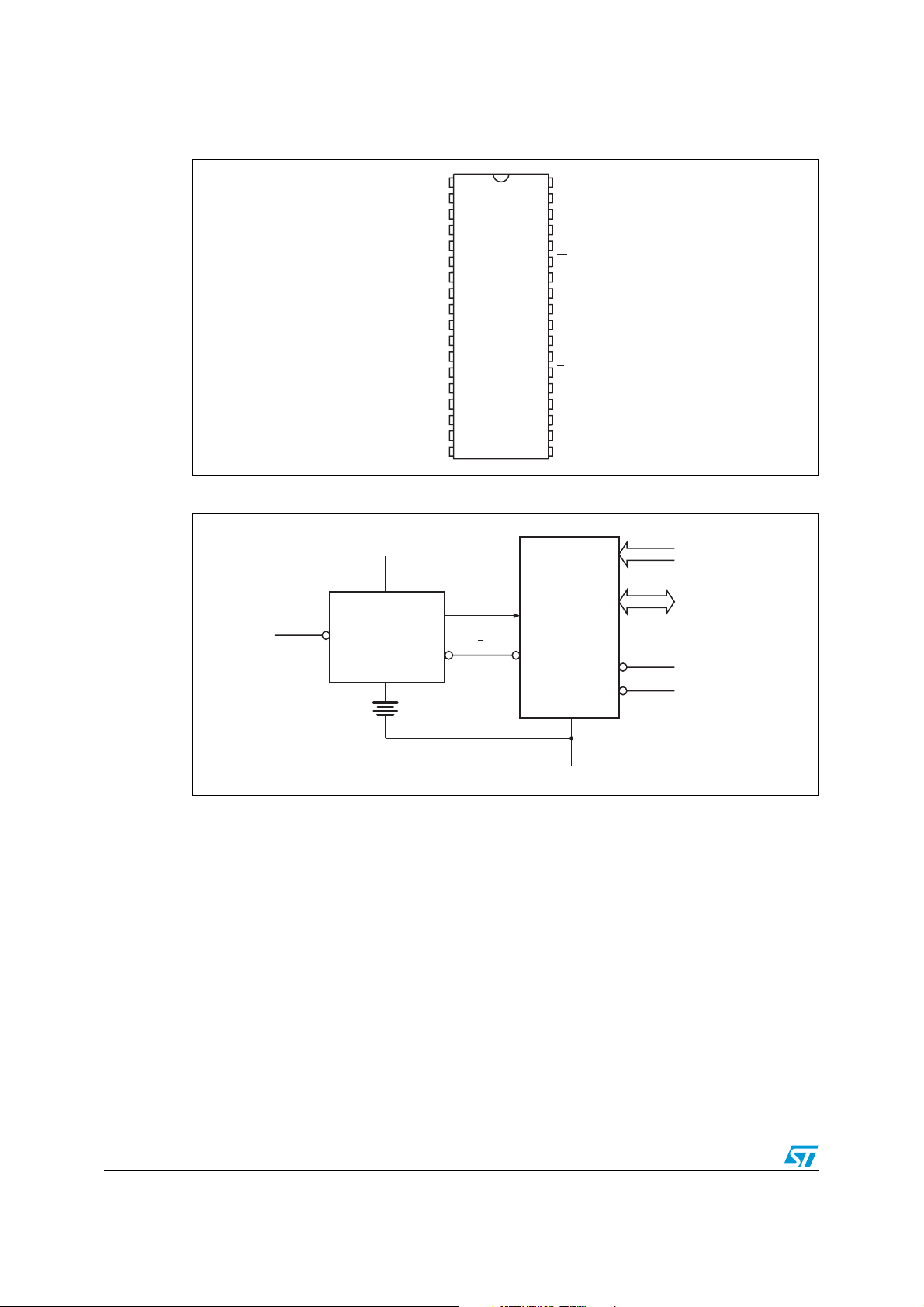
Figure 1. Logic diagram
V
CC
Table 1. Signal names
A0-A20 Address inputs
DQ0-DQ7 Data inputs / outputs
E Chip enable
G Output enable
W WRITE enable
V
CC
V
SS
NC Not connected internally
21
A0-A20
W
E
G
Supply voltage
Ground
M48Z2M1Y
M48Z2M1V
V
SS
8
DQ0-DQ7
AI02048
Doc ID 5135 Rev 6 5/20
Description M48Z2M1Y, M48Z2M1V
Figure 2. DIP connections
Figure 3. Block diagram
E
VOLTAGE SENSE
SWITCHING
CIRCUITRY
V
CC
AND
NC
A20
A18
A16
A14
A12
A7
A6
A5
A4
A3
A2
A1
A0
DQ0
DQ2
V
SS
INTERNAL
BATTERIES
1
2
3
4
5
6
7
8
M48Z2M1Y
9
M48Z2M1V
10
11
12
13
14
15
16
17
18
POWER
E
V
36
CC
A19
35
34
NC
A15
33
A17
32
W
31
A13
30
A8
29
A9
28
27
A11
G
26
A10
25
E
24
DQ7
23
DQ6
22
DQ5DQ1
21
DQ4
20
DQ3
19
2048K x 8
SRAM ARRAY
AI02049
A0-A20
DQ0-DQ7
W
G
6/20 Doc ID 5135 Rev 6
V
SS
AI02050
 Loading...