


查询M48T58Y-70MH1供应商
5.0V, 64 Kbit (8 Kb x 8) TIMEKEEPER®SRAM
FEATURES SUMMARY
■ INTEGRATED, ULTRA LOW POWER SRAM,
REAL TIMECLOCK, POWER-FAILCONTROL
CIRCUIT and BATTERY
■ BYTEWIDE™ RAM-LIKE CLO CK A CCESS
■ BCD CODED YEAR, MONTH, DAY, DATE,
HOURS, MINUTES, and SE CONDS
■ FREQUENCY TEST OUTPUT FOR REAL
TIME CLOCK
■ AUTOMATIC POWER-FAIL CHIP DESELECT
and WRITE PROTECTION
■ WRITE PROTECT VOLTAGES
(V
= Power-fail Deselect V oltage):
PFD
– M48T58: V
4.5V ≤ V
– M48T58Y: V
4.2V ≤ V
■ SELF-CONTAINED BATTERY and CRYSTAL
IN THE CAPHAT™ DIP PACKAGE
■ PACKAGINGINCLUDESa28-LEADSOICand
SNAPHAT
■ SOIC PACKAGE PROVIDES DIRECT
CONNECTION FOR A SNAPHAT HOUSING
CONTAINING THE BATTERY and CRYSTAL
■ PIN and FUNCTION COMPATIBLE WITH
JEDEC STANDARD 8 Kb x 8 SRAMs
= 4.75 to 5.5V
CC
≤ 4.75V
PFD
= 4.5 to 5.5V
CC
≤ 4.5V
PFD
®
TOP (to be Ordered Separately)
M48T58
M48T58Y
Figure 1. 28-pin P CDI P, CAPHAT™ Package
28
1
PCDIP28 (PC)
Battery/Crystal
CAPHAT
Figure 2. 28-pin SOIC Package
SNAPHAT (SH)
Battery/Crystal
28
SOH28 (MH)
1
1/27May 2002

M48T58, M48T58Y
TABLE OF CONTENTS
SUMMARYDESCRIPTION...........................................................4
LogicDiagram(Figure3.).........................................................4
SignalNames(Table1.)..........................................................4
DIP Connect ions (Figure 4.) .......................................................5
SOIC Connections (Fig ure 5.)......................................................5
BlockDiagram(Figure6.).........................................................5
MAXIMUMRATING.................................................................6
AbsoluteMaximumRatings(Table2.) ...............................................6
DC AND AC PARAMETERS. . ........................................................7
Operating and AC Measurement Conditions (Tabl e 3.) ..................................7
ACMeasurementLoadCircuit(Figure7.).............................................7
Capacitance (Table 4. ) . . . ........................................................7
DCCharacteristics(Table5.) ......................................................8
OPERATIONMODES...............................................................9
Operating Modes (Table 6.)........................................................9
READMode...................................................................10
READModeACWaveforms(Figure8.).............................................10
READModeACCharacteristics(Table7.)...........................................11
WRITEMode..................................................................12
WRITE Enable Controlled, WRITE AC Waveform (Figure 9.).............................12
ChipEnableControlled,WRITEACWaveforms(Figure10.).............................13
WRITEModeACCharacteristics(Table8.)..........................................14
DataRetentionMode............................................................15
PowerDown/UpModeACWaveforms(Figure11.)....................................15
PowerDown/UpACCharacteristics(Table9.)........................................16
PowerDown/UpTripPointsDCCharacteristics(Table10.)..............................16
2/27

M48T58, M 48T 58Y
CLOCKOPERATIONS.............................................................17
Reading the Clock. .............................................................17
RegisterMap(Table11.).........................................................17
SettingtheClock...............................................................17
Stopping and S tarting the Oscillator ................................................17
CalibratingtheClock............................................................18
BatteryLowFlag...............................................................19
CenturyBit....................................................................19
CrystalAccuracyAcrossTemperature(Figure12.) ....................................19
ClockCalibration(Figure13.).....................................................20
V
Noise And Negative Going Transients. ..........................................20
CC
SupplyVoltageProtection(Figure14.)..............................................20
PARTNUMBERING ...............................................................21
SNAPHATBatteryTable(Table13.)................................................21
PACKAGE MECHANICAL INFORMATION . . . ..........................................22
REVISIONHISTORY...............................................................26
3/27
M48T58, M48T58Y
SUMMARY DESCRIPTION
®
The M48T58/Y TIMEKEEPER
non-volatile static RAM and real time clock . The
monolithic chip is available in two special pack agesto providea highly integrated battery backed-up
memory and real time clock solution.
The M48T58 /Y is a non-volatile pin and func tion
equivalent toany JEDEC s tandard 8Kbx 8 SR AM.
It also easily fits into many ROM, EPROM, and
EEPROM sockets, providing the non-volatility of
PROMs without any requirement for special
WRITE timing or limitations on the number of
WRITEs that can be performed.
The 28-pin, 600mil DIP CAPHAT™ houses the
M48T58/Y silicon with a quartz crystal and a long
life lithium button cell in a single package.
RAM is a 8Kb x 8
The 28-pin, 330mil SOIC provides sockets with
gold plated contacts at both ends for direct connection to a separate SNAPHAT
taining the battery and crystal. The unique design
allows the SNAPHAT battery pac k age to be
mounted on top of the SOIC package after the
completion of the surface mount process. Insertion of the SNAPHAT housing after reflow prevents potential battery and crystal damage due to
the high temperatures required for device surfacemounting. The S NAPHAT housing is keyed to prevent rev ers e insertion. The S OI C and battery/crystal packages are shipped separatelyin plastic antistatic tubes or in Tape & Reel form.
For the 28-lead SOIC, the battery/crystal package
(e.g., SNAPHAT) part number is “M4T 28BR12SH” (see Table 13, page 21).
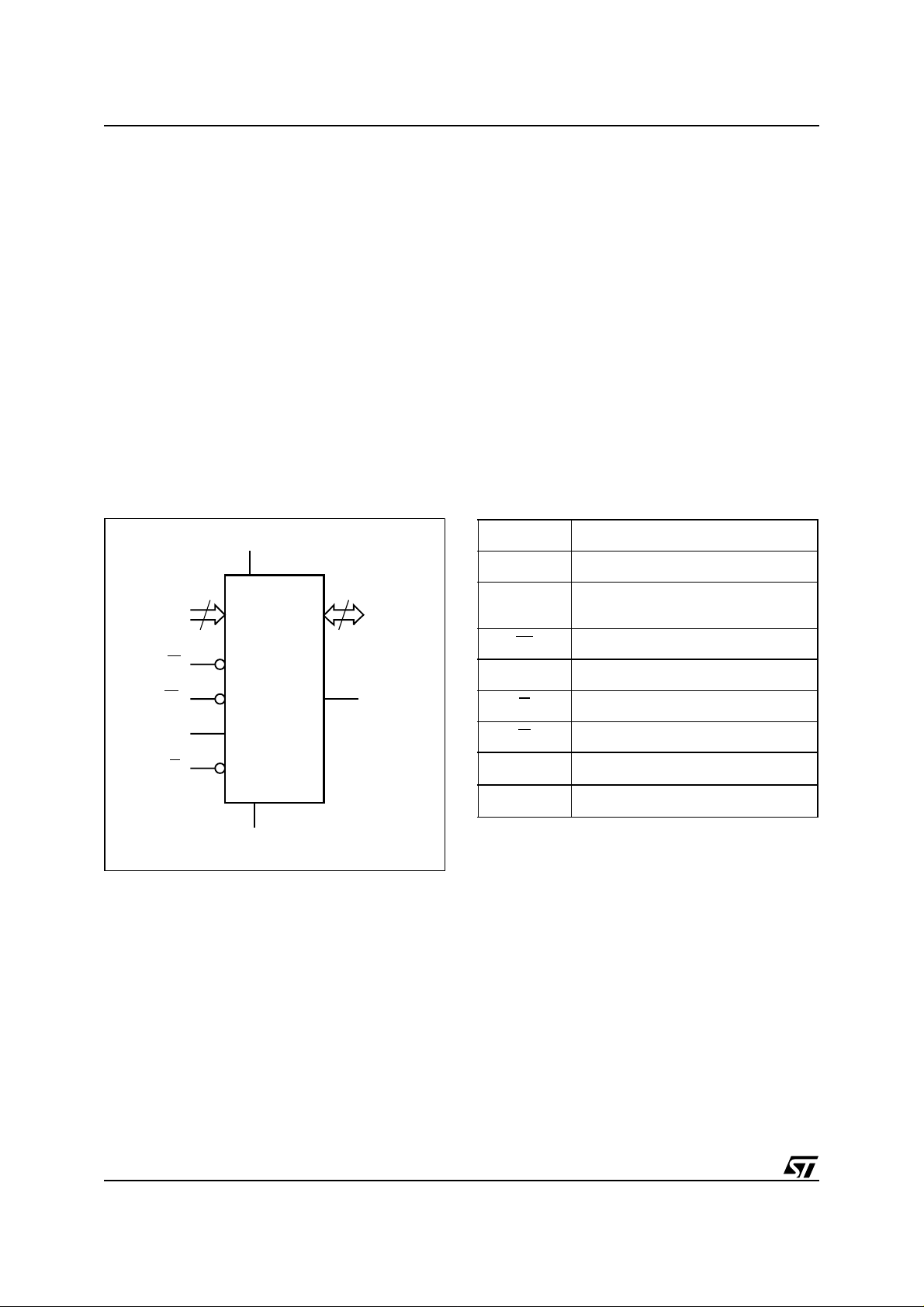
Figure 3. Logic Diagram Table 1. Signal Names
A0-A12 Address Inputs
DQ0-DQ7 Data Inputs / Outputs
FT
Frequency Test Output (Open
Drain)
A0-A12
13
V
CC
8
DQ0-DQ7
®
housing con-
W
E1 FT
E2
G
M48T58
M48T58Y
V
SS
AI01374B
E1
E2 Chip Enable 2
G
W
V
CC
V
SS
Chip Enable 1
Output Enable
WRITE Enable
Supply Voltage
Ground
4/27

M48T58, M 48T 58Y
Figure 4. DIP Connections Figure 5. SOIC Connections
FT V
1
A12
2
A7
3
A6
4
A5
5
6
A4
7
A3
A2
A1
A0
DQ0
8
M48T58Y
9
10
11
M48T58
12
DQ2
13
14
SS
Figure 6. Block Diagram
32,768 Hz
CRYSTAL
28
CC
W
27
26
E2
25
A8
24
A9
23
A11
22
G
21
A10
20
E1
19
DQ7
18
DQ6
17
DQ5DQ1
DQ4
16
DQ3V
15
AI01375B
FT
OSCILLATOR AND
CLOCK CHAIN
FT V
A12
A7
A6
A5
A4
A3
A2
A1
A0
DQ0
1
2
3
4
5
6
7
8
9
10
11
M48T58Y
12
DQ2
SS
13
14
8 x 8 BiPORT
SRAM ARRAY
28
27
26
25
24
23
22
21
20
19
18
17
16
15
AI01376B
CC
W
E2
A8
A9
A11
G
A10
E1
DQ7
DQ6
DQ5DQ1
DQ4
DQ3V
A0-A12
LITHIUM
CELL
VOLTAGE SENSE
AND
SWITCHING
CIRCUITRY
V
CC
POWER
V
PFD
8184 x 8
SRAM ARRAY
V
SS
DQ0-DQ7
E1
E2
W
G
AI01377C
5/27

M48T58, M48T58Y
MAXIMUM RATING
Stressingthedeviceabovetheratinglistedinthe
“Absolute Maxim um Ratings” table may cause
permanent damage to the dev ice. These are
stress ratings only and operation of the device at
these or any other conditions a bove those indicated in the Operating sections of this specification is
Table 2. Absolute Maximum Ratings
Symbol Parameter Value Unit
T
A
T
STG
(1,2)
T
SLD
V
IO
V
CC
I
O
P
D
Note: 1. For DIP package: Soldering temperature not to exceed 260°C for 10 seconds (total thermal budget not to exceed 150°C for longer
than 30 seconds).
2. For SO package: Reflow at peak temperature of 215°C to 225°C for < 60 seconds (total thermal budget not to exceed 180°C for
between 90 to 120 seconds).
CAUTION: Negative undershoots below –0.3V are not allowed on any pin while in the Battery Back-up mode.
CAUTION: Do NOT wave solder SOICto avoid damaging SNAPHAT sockets.
Ambient Operating Temperature 0 to 70 °C
Storage Temperature (VCCOff, Oscillator Off)
Lead Solder Temperature for 10 seconds 260 °C
Input or Output Voltages –0.3 to 7 V
Supply Voltage –0.3 to 7 V
Output Current 20 mA
Power Dissipation 1 W
not implied. Expos ure to Absolute Maximum Rating conditions for extended periods may affect device reliability. Refer also to the
STMicroelectronics SURE Program and other relevant quality documents.
–40 to 85 °C
6/27

DC AND AC PARAMETERS
This s ec t ion summarizes the operating and measurement con ditions, as w ell as t he DC and AC
characteristics of the device. The parameters in
the following DC and AC Characteristic tables are
derived from tests performed under the Measure-
Table 3. Operating and AC Measurement Conditions
Parameter M48T58 M48T58Y Unit
M48T58, M 48T 58Y
ment Conditions listed in the relevant tables. Designers should check that the operating condit ions
in their projects match the measurement conditions when using t he quoted parameters.
Supply Voltage (V
Ambient Operating Temperature (T
Load Capacitance (C
CC
)
)
A
)
L
4.75 to 5.5 4.5 to 5.5 V
0 to 70 0 to 70 °C
100 100 pF
Input Rise and Fall Times ≤ 5 ≤ 5ns
Input Pulse Voltages 0 to 3 0 to 3 V
Input and Output Timing Ref. Voltages 1.5 1.5 V
Note: Output Hi-Z is defined as the point where data is no longer driven.
Figure 7. AC Measurement Load Circuit
5V
1.9kΩ
DEVICE
UNDER
TEST
1kΩ
OUT
CL = 100pF or 5pF
CL includes JIG capacitance
AI01030
Table 4. Capacitance
Symbol
C
IN
(3)
C
OUT
Note: 1. Effective capacitance measured with power supply at 5V; sampled only, not 100% tested.
2. At 25°C, f = 1MHz.
3. Outputs deselected.
Input Capacitance 10 pF
Output Capacitance 10 pF
Parameter
(1,2)
Min Max Unit
7/27

M48T58, M48T58Y
Table 5. DC C haracteristics
Symbol Parameter
Test Condition
(1)
M48T58 M48T58Y
Min Max Min Max
Unit
Input Leakage Current
I
LI
(2)
I
LO
I
I
CC1
I
CC2
V
V
Output Leakage Current
Supply Current Outputs open 50 50 mA
CC
Supply Current (Standby)
TTL
Supply Current (Standby)
CMOS
(3)
Input Low Voltage –0.3 0.8 –0.3 0.8 V
IL
Input High Voltage 2.2
IH
0V ≤ V
0V ≤ V
E1
E2=V
Output Low Voltage
V
OL
Output Low Voltage (FT)
V
Note: 1. ValidforAmbientOperatingTemperature: TA=0to70°C;VCC= 4.75 to 5.5V or 4.5 to 5.5V (except where noted).
Output High Voltage
OH
2. Outputs deselected.
3. Negativespikes of –1V allowed forup to 10ns onceper Cycle.
4. The FT pin is Open Drain.
(4)
≤ V
IN
≤ V
OUT
=V
E1
IH
E2 = V
IO
=VCC– 0.2V
+ 0.2V
SS
I
= 2.1mA
OL
IOL= 10mA
I
=–1mA
OH
CC
CC
±1 ±1 µA
±1 ±1 µA
33mA
33mA
V
CC
+ 0.3
2.2
VCC+0.3
0.4 0.4
0.4 0.4 V
2.4 2.4 V
V
8/27

OPERATION MODES
As Figure 6, page 5 shows, the static memory array and the quartz controlled clock oscillator of the
M48T58/Y are integrated on one silicon chip. The
two circuits are interconnected at the upper eight
memory locations to p rovide user acce ssible
BYTEWIDE™ clock information in the bytes with
addresses 1FF8h-1FFFh. The clock locations
contain the century, year, month, date, day, hour,
minute, and second in 24 hour BC D format (except
for the c entury). Corrections for 28, 29 (leap year valid until 2100), 30, and 31 day m onths are made
automatically. Byte 1FF8h is the clock control register. This byte controls user access to th e clock
information and also stores the clock calibration
setting.
The eight clock bytes are not the actual clock
counters themselves; t hey are memory locations
Table 6. Operating Modes
Mode
Deselect
Deselect X
WRITE
READ
READ
Deselect
Deselect
Note: X = VIHor VIL;VSO= Battery Back-up Switchover Voltage.
1. See Table 10, page 16 for details.
VSOto V
V
CC
4.75 to 5.5V
or
4.5 to 5.5V
(min)
PFD
(1)
≤ V
SO
E1 E2 G W DQ0-DQ7 Power
(1)
V
IH
V
IL
V
IL
V
IL
X X X X High Z CMOS Standby
X X X X High Z Battery Back-up Mode
X X X High Z Standby
V
IL
V
IH
V
IH
V
IH
M48T58, M 48T 58Y
consisting of BiPO RT™ READ/write memory
cells. The M48T58/Y includes a clock control circuit which updates t he clock bytes with current information once per second. The information can
be accessed by the user in the same manner as
any other location in the static memory array.
The M48T58/Y also has its own Power-fail Detect
circuit. The control c ircuitry constantly monitors
the single 5V supply for an out-of-tolerance condition. When V
protects the SRA M, providing a high degree of
data security in the midst of unpredictable system
operation brought on by low V
low the Bat tery Back-up Switchover Voltage
), the control circuitry connects the battery
(V
SO
which maintains data and clock operation until valid power returns.
X X High Z Standby
X
V
IL
V
IH
V
IL
V
IH
V
IH
is out of tolerance, the circuit write
CC
.AsVCCfalls be-
CC
D
IN
D
OUT
High Z Active
Active
Active
9/27
 Loading...