

M48T37Y
M48T37V
5.0 or 3.3 V, 256 Kbit (32 Kbit x 8) TIMEKEEPER® SRAM
Features
■ Integrated ultra low power SRAM, real-time
clock, power-fail control circuit, and battery
■ Frequency test output for real-time clock
software calibration
■ Automatic power-fail chip deselect and WRITE
protection
■ Watchdog timer
■ WRITE protect voltage
(V
= Power-fail deselect voltage):
PFD
–M48T37Y: V
4.2 V ≤ V
–M48T37V: V
2.7 V ≤ V
■ Packaging includes a 44-lead SOIC and
SNAPHAT
■ SOIC package provides direct connection for a
SNAPHAT
®
®
crystal
■ Microprocessor power-on reset (valid even
during battery backup mode)
■ Programmable alarm output active in the
battery backup mode
■ Battery low flag
■ RoHS compliant
– Lead-free second level interconnect
= 4.5 to 5.5 V
CC
≤ 4.5 V
PFD
= 3.0 to 3.6 V
CC
≤ 3.0 V
PFD
top (to be ordered separately)
top which contains the battery and
SNAPHAT® (SH)
Battery/crystal
44
1
SOH44 (MH)
44-pin SOIC
August 2010 Doc ID 7019 Rev 9 1/30
www.st.com
1

Contents M48T37Y, M48T37V
Contents
1 Description . . . . . . . . . . . . . . . . . . . . . . . . . . . . . . . . . . . . . . . . . . . . . . . . . 5
2 Operation modes . . . . . . . . . . . . . . . . . . . . . . . . . . . . . . . . . . . . . . . . . . . . 8
2.1 READ mode . . . . . . . . . . . . . . . . . . . . . . . . . . . . . . . . . . . . . . . . . . . . . . . . 8
2.2 WRITE mode . . . . . . . . . . . . . . . . . . . . . . . . . . . . . . . . . . . . . . . . . . . . . . 10
2.3 Data retention mode . . . . . . . . . . . . . . . . . . . . . . . . . . . . . . . . . . . . . . . . . 11
3 Clock operations . . . . . . . . . . . . . . . . . . . . . . . . . . . . . . . . . . . . . . . . . . . 12
3.1 Reading the clock . . . . . . . . . . . . . . . . . . . . . . . . . . . . . . . . . . . . . . . . . . . 12
3.2 Setting the clock . . . . . . . . . . . . . . . . . . . . . . . . . . . . . . . . . . . . . . . . . . . . 12
3.3 Stopping and starting the oscillator . . . . . . . . . . . . . . . . . . . . . . . . . . . . . 12
3.4 Setting the alarm clock . . . . . . . . . . . . . . . . . . . . . . . . . . . . . . . . . . . . . . . 14
3.5 Calibrating the clock . . . . . . . . . . . . . . . . . . . . . . . . . . . . . . . . . . . . . . . . . 15
3.6 Watchdog timer . . . . . . . . . . . . . . . . . . . . . . . . . . . . . . . . . . . . . . . . . . . . 16
3.7 Power-on reset . . . . . . . . . . . . . . . . . . . . . . . . . . . . . . . . . . . . . . . . . . . . . 17
3.8 Programmable interrupts . . . . . . . . . . . . . . . . . . . . . . . . . . . . . . . . . . . . . 17
3.9 Battery low flag . . . . . . . . . . . . . . . . . . . . . . . . . . . . . . . . . . . . . . . . . . . . . 18
3.10 Initial power-on defaults . . . . . . . . . . . . . . . . . . . . . . . . . . . . . . . . . . . . . . 18
3.11 V
noise and negative going transients . . . . . . . . . . . . . . . . . . . . . . . . . 18
CC
4 Maximum ratings . . . . . . . . . . . . . . . . . . . . . . . . . . . . . . . . . . . . . . . . . . . 20
5 DC and AC parameters . . . . . . . . . . . . . . . . . . . . . . . . . . . . . . . . . . . . . . 21
6 Package mechanical data . . . . . . . . . . . . . . . . . . . . . . . . . . . . . . . . . . . . 24
7 Part numbering . . . . . . . . . . . . . . . . . . . . . . . . . . . . . . . . . . . . . . . . . . . . 27
8 Environmental information . . . . . . . . . . . . . . . . . . . . . . . . . . . . . . . . . . . 28
9 Revision history . . . . . . . . . . . . . . . . . . . . . . . . . . . . . . . . . . . . . . . . . . . 29
2/30 Doc ID 7019 Rev 9

M48T37Y, M48T37V List of tables
List of tables
Table 1. Signal names . . . . . . . . . . . . . . . . . . . . . . . . . . . . . . . . . . . . . . . . . . . . . . . . . . . . . . . . . . . . 6
Table 2. Operating modes . . . . . . . . . . . . . . . . . . . . . . . . . . . . . . . . . . . . . . . . . . . . . . . . . . . . . . . . . 8
Table 3. READ mode AC characteristics . . . . . . . . . . . . . . . . . . . . . . . . . . . . . . . . . . . . . . . . . . . . . . 9
Table 4. WRITE mode AC characteristics . . . . . . . . . . . . . . . . . . . . . . . . . . . . . . . . . . . . . . . . . . . . 11
Table 5. Register map . . . . . . . . . . . . . . . . . . . . . . . . . . . . . . . . . . . . . . . . . . . . . . . . . . . . . . . . . . . 13
Table 6. Alarm repeat modes . . . . . . . . . . . . . . . . . . . . . . . . . . . . . . . . . . . . . . . . . . . . . . . . . . . . . . 14
Table 7. Default values . . . . . . . . . . . . . . . . . . . . . . . . . . . . . . . . . . . . . . . . . . . . . . . . . . . . . . . . . . . 18
Table 8. Absolute maximum ratings . . . . . . . . . . . . . . . . . . . . . . . . . . . . . . . . . . . . . . . . . . . . . . . . . 20
Table 9. Operating and AC measurement conditions . . . . . . . . . . . . . . . . . . . . . . . . . . . . . . . . . . . . 21
Table 10. Capacitance . . . . . . . . . . . . . . . . . . . . . . . . . . . . . . . . . . . . . . . . . . . . . . . . . . . . . . . . . . . . 21
Table 11. DC characteristics. . . . . . . . . . . . . . . . . . . . . . . . . . . . . . . . . . . . . . . . . . . . . . . . . . . . . . . . 22
Table 12. Power down/up AC characteristics . . . . . . . . . . . . . . . . . . . . . . . . . . . . . . . . . . . . . . . . . . . 23
Table 13. Power down/up trip points DC characteristics . . . . . . . . . . . . . . . . . . . . . . . . . . . . . . . . . . 23
Table 14. SOH44 – 44-lead plastic small outline, 4-socket SNAPHAT
Table 15. SH – 4-pin SNAPHAT
Table 16. SH – 4-pin SNAPHAT
Table 17. Ordering information scheme . . . . . . . . . . . . . . . . . . . . . . . . . . . . . . . . . . . . . . . . . . . . . . . 27
Table 18. SNAPHAT® battery table . . . . . . . . . . . . . . . . . . . . . . . . . . . . . . . . . . . . . . . . . . . . . . . . . . 27
Table 19. Document revision history . . . . . . . . . . . . . . . . . . . . . . . . . . . . . . . . . . . . . . . . . . . . . . . . . 29
®
housing for 48 mAh battery & crystal, package mechanical data . 25
®
housing for 120 mAh battery & crystal, package mechanical data26
®
, package mechanical data . 24
Doc ID 7019 Rev 9 3/30

List of figures M48T37Y, M48T37V
List of figures
Figure 1. Logic diagram . . . . . . . . . . . . . . . . . . . . . . . . . . . . . . . . . . . . . . . . . . . . . . . . . . . . . . . . . . . . 5
Figure 2. SOIC connections . . . . . . . . . . . . . . . . . . . . . . . . . . . . . . . . . . . . . . . . . . . . . . . . . . . . . . . . . 6
Figure 3. Block diagram . . . . . . . . . . . . . . . . . . . . . . . . . . . . . . . . . . . . . . . . . . . . . . . . . . . . . . . . . . . . 7
Figure 4. READ mode AC waveforms . . . . . . . . . . . . . . . . . . . . . . . . . . . . . . . . . . . . . . . . . . . . . . . . . 9
Figure 5. WRITE enable controlled, WRITE AC waveform . . . . . . . . . . . . . . . . . . . . . . . . . . . . . . . . 10
Figure 6. Chip enable controlled, WRITE AC waveforms . . . . . . . . . . . . . . . . . . . . . . . . . . . . . . . . . 10
Figure 7. Alarm interrupt reset waveform . . . . . . . . . . . . . . . . . . . . . . . . . . . . . . . . . . . . . . . . . . . . . . 14
Figure 8. Backup mode alarm waveforms . . . . . . . . . . . . . . . . . . . . . . . . . . . . . . . . . . . . . . . . . . . . . 15
Figure 9. Supply voltage protection . . . . . . . . . . . . . . . . . . . . . . . . . . . . . . . . . . . . . . . . . . . . . . . . . . 19
Figure 10. Crystal accuracy across temperature . . . . . . . . . . . . . . . . . . . . . . . . . . . . . . . . . . . . . . . . . 19
Figure 11. Clock calibration . . . . . . . . . . . . . . . . . . . . . . . . . . . . . . . . . . . . . . . . . . . . . . . . . . . . . . . . . 19
Figure 12. AC testing load circuit . . . . . . . . . . . . . . . . . . . . . . . . . . . . . . . . . . . . . . . . . . . . . . . . . . . . . 21
Figure 13. Power down/up mode AC waveforms. . . . . . . . . . . . . . . . . . . . . . . . . . . . . . . . . . . . . . . . . 22
Figure 14. SOH44 – 44-lead plastic small outline, 4-socket SNAPHAT
Figure 15. SH – 4-pin SNAPHAT
Figure 16. SH – 4-pin SNAPHAT
Figure 17. Recycling symbols . . . . . . . . . . . . . . . . . . . . . . . . . . . . . . . . . . . . . . . . . . . . . . . . . . . . . . . 28
®
housing for 48 mAh battery & crystal, pack. outline . . . . . . . . . . . 25
®
housing for 120 mAh battery & crystal, pack. outline . . . . . . . . . . 26
®
outline. . . . . . . . . . . . . . . . . 24
4/30 Doc ID 7019 Rev 9
M48T37Y, M48T37V Description
1 Description
The M48T37Y/V TIMEKEEPER® RAM is a 32 Kb x 8 non-volatile static RAM and real-time
clock. The monolithic chip is available in a special package which provides a highly
integrated battery-backed memory and real-time clock solution.
The 44-lead, 330 mil SOIC package provides sockets with gold-plated contacts at both ends
for direct connection to a separate SNAPHAT housing containing the battery and crystal.
The unique design allows the SNAPHAT
the SOIC package after the completion of the surface mount process.
Insertion of the SNAPHAT housing after reflow prevents potential battery and crystal
damage due to the high temperatures required for device surface-mounting. The SNAPHAT
housing is keyed to prevent reverse insertion.
The SOIC and battery packages are shipped separately in plastic anti-static tubes or in tape
& reel form. For the 44-lead SOIC, the battery/crystal package (e.g., SNAPHAT) part
number is “M4T28-BR12SH” or “M4T32-BR12SH”.
Caution: Do not place the SNAPHAT battery/crystal top in conductive foam, as this will drain the
lithium button-cell battery.
Figure 1. Logic diagram
®
battery/crystal package to be mounted on top of
A0-A14
W
WDI
V
CC
15
M48T37Y
E
G
M48T37V
V
SS
8
DQ0-DQ7
RST
IRQ/FT
AI02172
Doc ID 7019 Rev 9 5/30
Description M48T37Y, M48T37V
Table 1. Signal names
A0-A14 Address inputs
DQ0-DQ7 Data inputs / outputs
RST Reset output (open drain)
IRQ/FT Interrupt / frequency test output (open drain)
WDI Watchdog input
E Chip enable
G Output enable
W WRITE enable
V
CC
V
SS
Supply voltage
Ground
NC Not connected internally
Figure 2. SOIC connections
NC
RST
NC
NC
A14
A12
A7
A6
A5
A4
A3
NC
NC
WDI
A2
A1
A0
DQ0
DQ2
NC
V
SS
1
2
3
4
5
6
7
8
9
10
11
12
13
14
15
16
17
18
19
20
21
22
M48T37Y
M48T37V
44
43
42
41
40
39
38
37
36
35
34
33
32
31
30
29
28
27
26
25
24
23
V
CC
NC
NC
NC
IRQ/FT
W
A13
A8
A9
A11
G
NC
NC
A10
E
NC
DQ7
DQ6
DQ5DQ1
DQ4
DQ3
NC
AI02174
6/30 Doc ID 7019 Rev 9
M48T37Y, M48T37V Description
Figure 3. Block diagram
IRQ/FT WDI
OSCILLATOR AND
CLOCK CHAIN
32,768 Hz
CRYSTAL
POWER
16 x 8 BiPORT
SRAM ARRAY
A0-A14
LITHIUM
CELL
VOLTAGE SENSE
AND
SWITCHING
CIRCUITRY
CC
RSTV
V
PFD
32,752 x 8
SRAM ARRAY
V
SS
DQ0-DQ7
E
W
G
AI03253
Doc ID 7019 Rev 9 7/30
Operation modes M48T37Y, M48T37V
2 Operation modes
As Figure 3 on page 7 shows, the static memory array and the quartz controlled clock
oscillator of the M48T37Y/V are integrated on one silicon chip. The memory locations that
provide user accessible BYTEWIDE™ clock information are in the bytes with addresses
7FF1 and 7FF9h-7FFFh (located in Table 5 on page 13). The clock locations contain the
century, year, month, date, day, hour, minute, and second in 24-hour BCD format.
Corrections for 28, 29 (leap year - valid until the year 2100), 30, and 31 day months are
made automatically.
Byte 7FF8h is the clock control register. This byte controls user access to the clock
information and also stores the clock calibration setting.
Byte 7FF7h contains the watchdog timer setting. The watchdog timer redirects an out-ofcontrol microprocessor and provides a reset or interrupt to it. Bytes 7FF2h-7FF5h are
reserved for clock alarm programming. These bytes can be used to set the alarm. This will
generate an active low signal on the IRQ
hours, minutes, and seconds of the clock. The eight clock bytes are not the actual clock
counters themselves; they are memory locations consisting of BiPORT™ READ/WRITE
memory cells. The M48T37Y/V includes a clock control circuit which updates the clock bytes
with current information once per second. The information can be accessed by the user in
the same manner as any other location in the static memory array.
/FT pin when the alarm bytes match the date,
The M48T37Y/V also has its own power-fail detect circuit. The control circuitry constantly
monitors the single V
tolerance, the circuit write protects the SRAM, providing a high degree of data security in the
midst of unpredictable system operation brought on by low V
battery backup switchover voltage (V
maintains data and clock operation until valid power returns.
Table 2. Operating modes
Mode V
Deselect
WRITE V
READ V
READ V
Deselect V
Deselect ≤ V
1. See Table on page 23 for details.
Note: X = V
or VIL; VSO = Battery backup switchover voltage.
IH
SO
2.1 READ mode
The M48T37Y/V is in the READ mode whenever WRITE enable (W) is high and chip enable
(E
) is low. The unique address specified by the 15 address inputs defines which one of the
32,752 bytes of data is to be accessed. Valid data will be available at the data I/O pins within
address access time (t
and output enable (G
supply for an out of tolerance condition. When VCC is out of
CC
. As VCC falls below the
CC
IN
D
OUT
High Z Active
Active
Active
CC
4.5 to 5.5 V
or
3.0 to 3.6 V
to V
PFD
SO
AVQ V
(min)
(1)
), the control circuitry connects the battery which
SO
E G W DQ0-DQ7 Power
X X High Z Standby
XVILD
V
V
V
IL
IH
IH
V
IH
(1)
V
IH
IL
IL
IL
X X X High Z CMOS standby
X X X High Z Battery backup mode
) after the last address input signal is stable, providing that the E
) access times are also satisfied. If the E and G access times are not
8/30 Doc ID 7019 Rev 9
M48T37Y, M48T37V Operation modes
met, valid data will be available after the latter of the chip enable access time (t
output enable access time (t
The state of the eight three-state data I/O signals is controlled by E
activated before t
, the data lines will be driven to an indeterminate state until t
AVQ V
If the address inputs are changed while E
for output data hold time (t
AXQX
).
GLQV
and G. If the outputs are
and G remain active, output data will remain valid
) but will be indeterminate until the next address access.
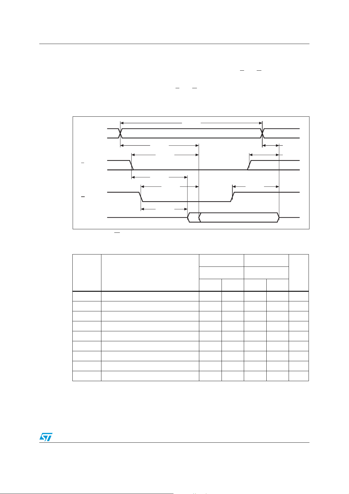
Figure 4. READ mode AC waveforms
tAVAV
A0-A14
tAVQV tAXQX
tELQV
E
tELQX
tGLQV
G
tGLQX
DQ0-DQ7
VAL ID
tGHQZ
VAL ID
ELQV
) or
AVQ V
tEHQZ
AI00925
.
Note: WRITE enable (W
Table 3. READ mode AC characteristics
Symbol Parameter
t
AVAV
t
AVQ V
t
ELQV
t
GLQV
t
ELQX
t
GLQX
t
EHQZ
t
GHQZ
t
AXQX
1. Valid for ambient operating temperature: TA = 0 to 70 °C or –40 to 85 °C; VCC = 4.5 to 5.5 V or 3.0 to 3.6 V
(except where noted).
2. CL = 5 pF.
READ cycle time 70 100 ns
Address valid to output valid 70 100 ns
Chip enable low to output valid 70 100 ns
Output enable low to output valid 35 50 ns
(2)
Chip enable low to output transition 5 10 ns
(2)
Output enable low to output transition 5 5 ns
(2)
Chip enable high to output Hi-Z 25 50 ns
(2)
Output enable high to output Hi-Z 25 40 ns
Address transition to output transition 10 10 ns
) = high.
(1)
M48T37Y M48T37V
Unit–70 –100
Min Max Min Max
Doc ID 7019 Rev 9 9/30
 Loading...