

ST M48T129Y, M48T129V User Manual
查询M48T129V-70CS1供应商
3.3V-5V 1 Mbit (128Kb x8) TIMEKEEPERSRAM
■ INTEGRATED ULTRA LOW POWER SRAM,
REAL TIME CLOCK, POWER-FAIL CONTROL
CIRCUIT, BATTERY ANDCRYSTAL
■ YEAR 2000 COMPLIANT
■ BCD CODED CENTURY, YEAR, MONTH,
DAY, DATE, HOURS, MINUTES, and
SECONDS
■ BATTERY LOW WARNING FLAG
■ AUTOMATIC POWER-FAIL CHIP DESELECT
and WRITE PROTECTION
■ TWO WRITE PROTECT VOLTAGES:
(V
= Power-fail Deselect Voltage)
PFD
– M48T129Y: 4.2V ≤ V
– M48T129V: 2.7V ≤ V
■ CONVENTIONAL SRAM OPERATION;
UNLIMITED WRITE CYCLES
■ SOFTWARE CONTROLLED CLOCK
CALIBRATION for HIGH ACCURACY
APPLICATIONS
■ 10 YEARS of DATA RETENTION and CLOCK
OPERATION in the ABSENCE of POWER
■ SELF CONTAINED BATTERY and CRYSTAL
in DIP PACKAGE
■ MICROPROCESSOR POWER-ON RESET
(Valid even during battery back-up mode)
■ PROGRAMMABLE ALARM OUTPUT ACTIVE
in BATTERY BACK-UP MODE
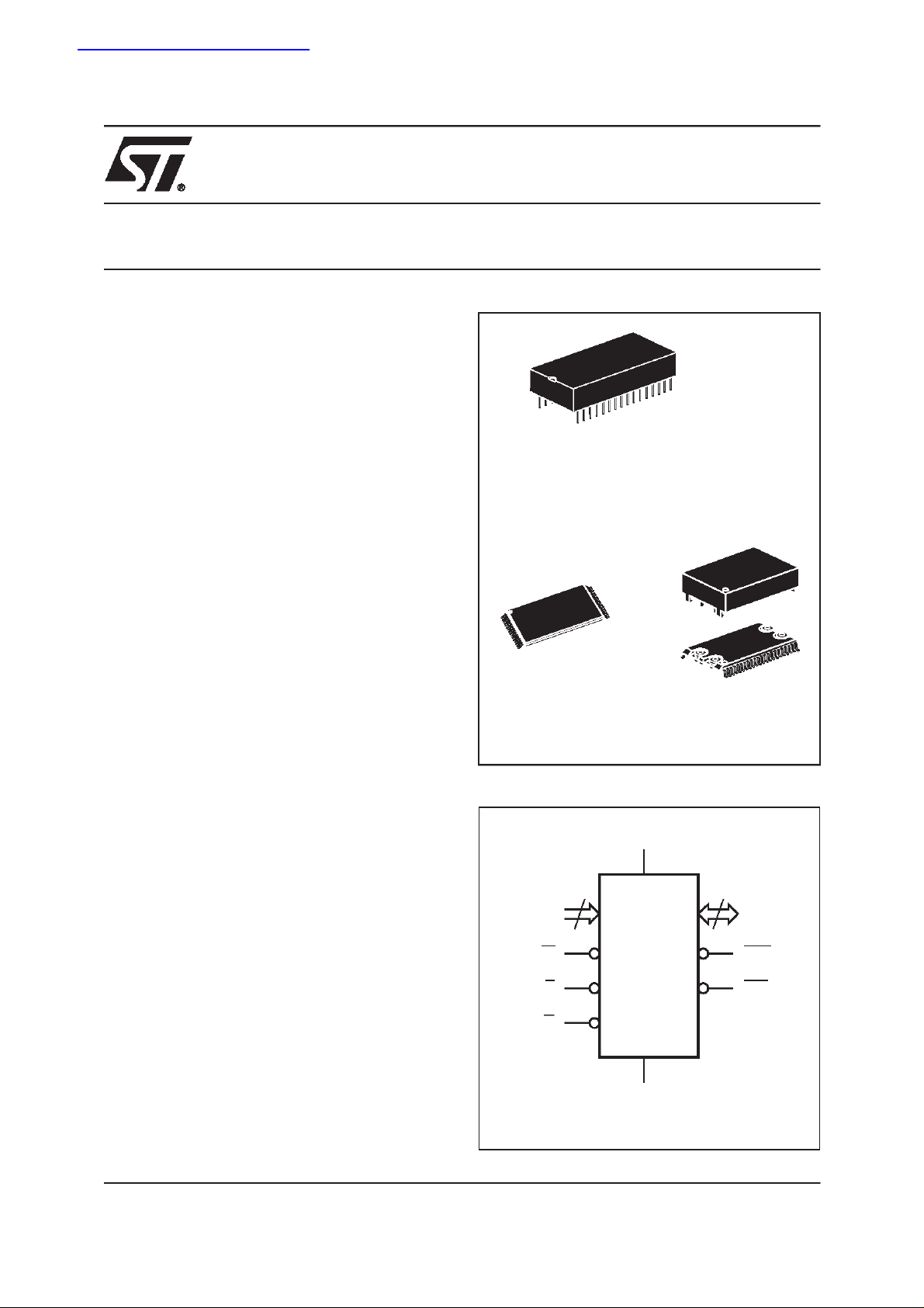
■ SURFACE MOUNT CHIP SET PACKAGING
INCLUDES a 44-PIN SOIC and a 32-LEAD
TSOP (SNAPHAT TOP TO BE ORDERED
SEPARATELY)
■ SOIC PACKAGE PROVIDES DIRECT
CONNECTION for a SNAPHAT TOP WHICH
CONTAINS the BATTERY and CRYSTAL
■ SNAPHAT
HOUSING (BATTERY/CRYSTAL)
IS REPLACEABLE
PFD
PFD
≤ 4.5V
≤ 3.0V
M48T129Y
M48T129V
32
1
PMDIP32(PM)
Module
SNAPHAT (SH)
Battery
TSOP32
(8 x 20mm)
Surface Mount Chip Set Solution (CS)
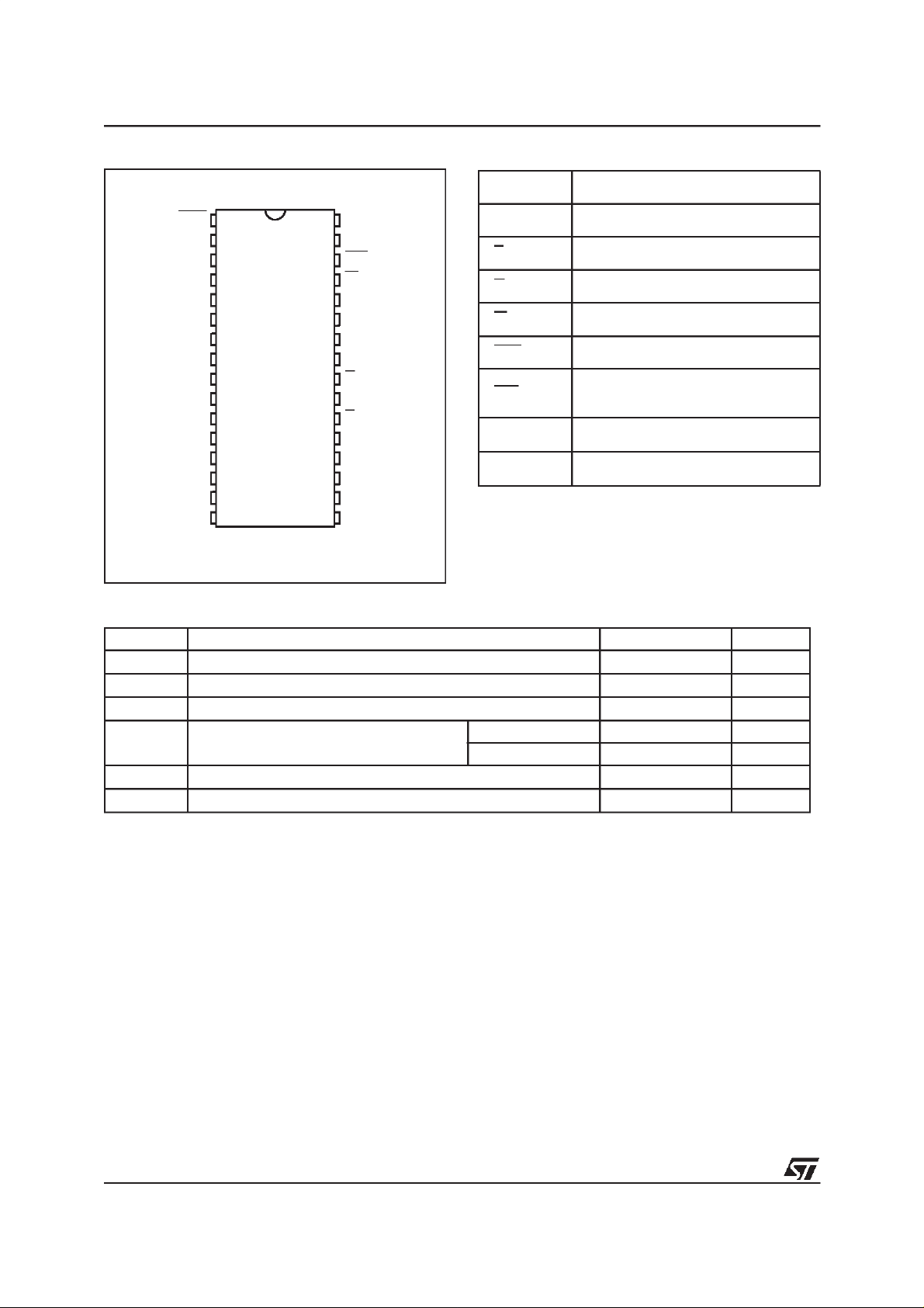
Figure 1. Logic Diagram
V
CC
17
A0-A16 DQ0-DQ7
W RST
E
G
M48T129Y
M48T129V
SOH44
8
IRQ/FT
V
SS
AI02260
1/22April 2000
M48T129Y, M48T129V
Figure 2. DIP Connections
RST V
1
A16
2
A14
A12
4
A7
5
A6
6
A5
7
A4
8
M48T129Y
A3
A2
A1
A0
DQ0
M48T129V
9
10
11
12
13
14
DQ2
15
16
SS
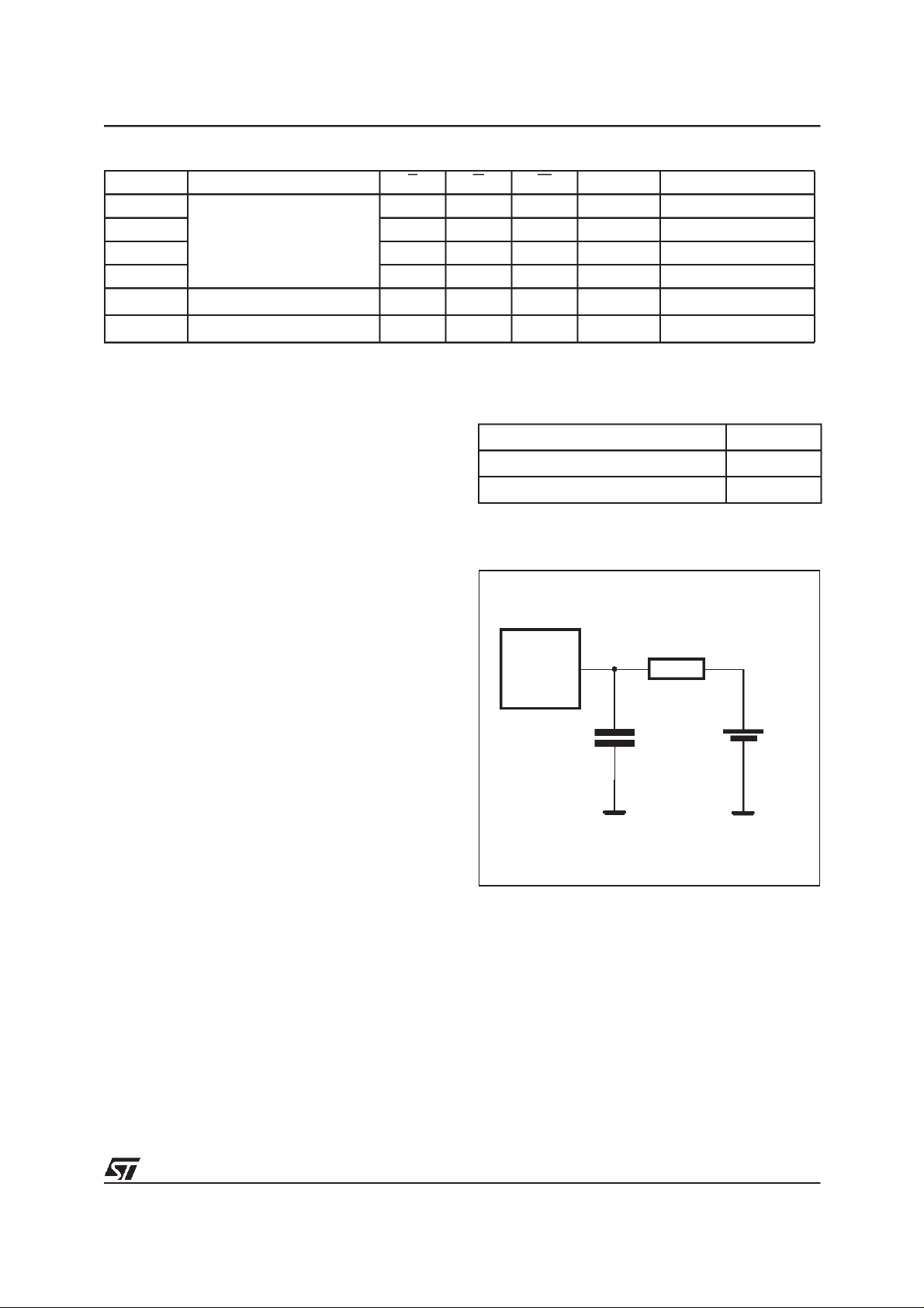
Table 2. Absolute Maximum Ratings
Symbol Parameter Value Unit
T
A
T
STG
V
IO
V
CC
I
O
P
Note: 1. Stresses greater than those listed under ”Absolute Maximum Ratings” may cause permanent damage to the device. Thisis a stress
2. Soldering temperature not to exceed 260°C for 10 seconds (total thermal budget not to exceed 150°C for longer than 30 seconds).
CAUTION: Negative undershoots below –0.3V are not allowed on any pin while in the Battery Back-up mode.
Ambient Operating Temperature 0 to 70 °C
Storage Temperature (VCCOff, Oscillator Off)
Input or Output Voltages
Supply Voltage
Output Current 20 mA
Power Dissipation 1 W
D
rating only and functional operation of the device at these or any other conditions above those indicated in the operational section
of this specification is not implied. Exposure to the absolute maximum rating conditions for extended periods of time may affect
reliability.
32
31
30
29
28
27
26
25
24
23
22
21
20
19
18
17
AI02261
CC
A15
IRQ/FT3
W
A13
A8
A9
A11
G
A10
E
DQ7
DQ6
DQ5DQ1
DQ4
DQ3V
(1)
Table 1. Signal Names
A0-A16 Address Inputs
DQ0-DQ7 Data Inputs / Outputs
E Chip Enable Input
G Output Enable Input
W Write Enable Input
RST Reset Output (open drain)
IRQ/FT
V
CC
V
SS
M48T129Y –0.3 to 7.0 V
M48T129V –0.3 to 4.6 V
Interrupt / Frequency Test Output
(open drain)
Supply Voltage
Ground
–40 to 85 °C
–0.3 to V
CC
+0.3
V
DESCRIPTION
The M48T129Y/V TIMEKEEPER RAM is a 128Kb
x 8 non-volatile static RAM and real time clock,
with programmable alarms and a watchdog timer.
The special DIP package provides a fully integrated battery back-up memoryandrealtime clock solution. The M48T129Y/V directly replaces industry
standard 128Kb x 8 SRAM. It also provides the
non-volatility of Flash without any requirement for
special write timing or limitations on the number of
writes that can be performed.
2/22
For surface mount environments ST provides a
Chip Set solution consisting of a 44 pin 330mil
SOIC TIMEKEEPER Supervisor (M48T201V/Y)
and a 32 pin TSOP (8 x 20mm) LPSRAM
(M68Z128/W) packages.
The 44 pin 330mil SOIC provides sockets with
gold plated contacts at both ends for direct connection to a separate SNAPHAT housing containing the battery.
The unique design allows the SNAPHAT battery
package to be mounted on top of the SOIC package after the completion of the surface mount pro-
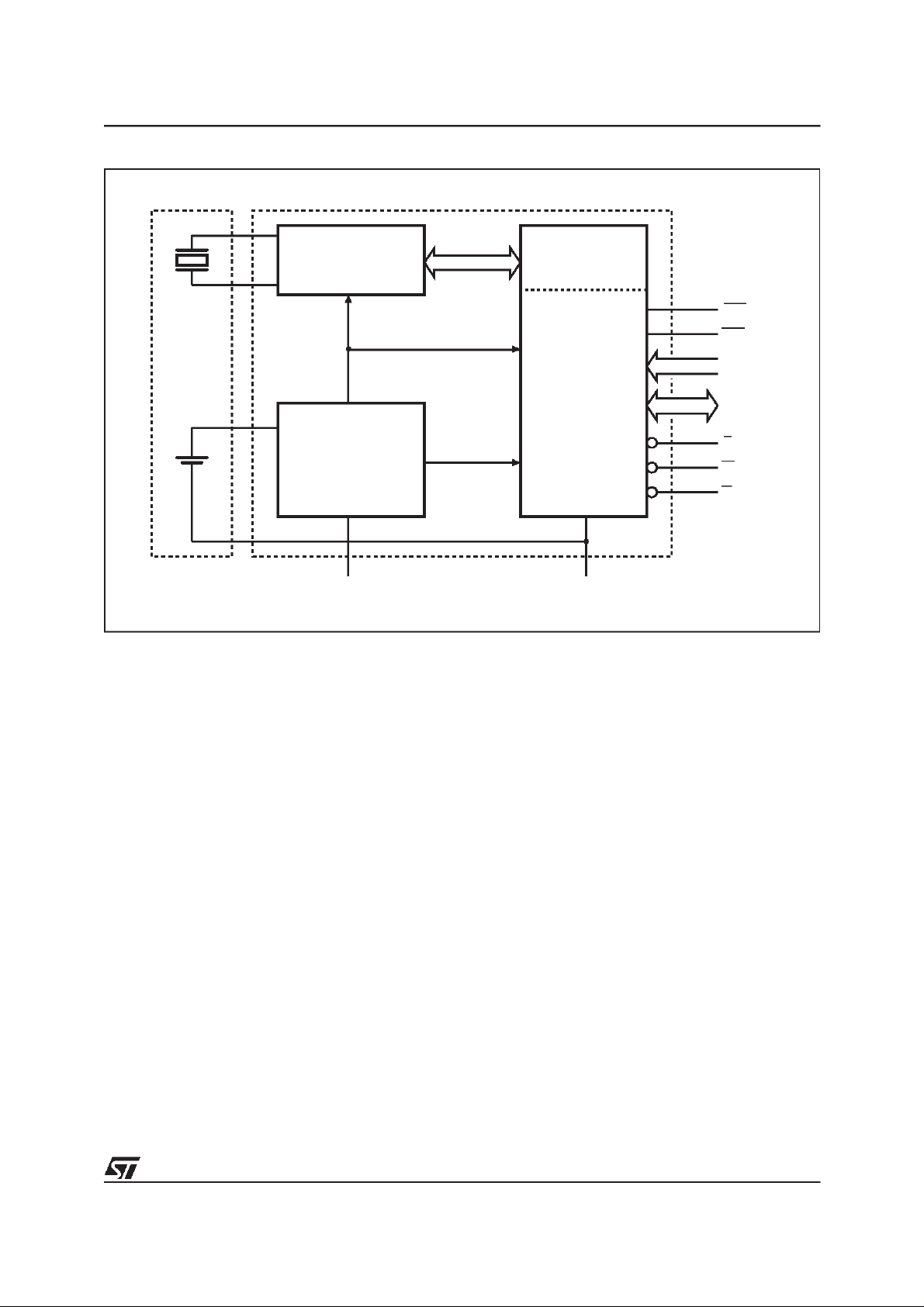
Figure 3. Block Diagram
M48T129Y, M48T129V
AND
V
CC
AND
POWER
SENSE
32,768
Hz
CRYSTAL
LITHIUM
CELL
OSCILLATOR
CLOCK CHAIN
VOLTAGE
SWITCHING
CIRCUITRY
cess. Insertion of the SNAPHAT housing after
reflow prevents potential battery damage due to
the hightemperatures required for device surfacemounting. The SNAPHAT housing is keyed to prevent reverse insertion.
The SNAPHAT battery package is shipped separately in plastic anti-static tubes or in Tape & Reel
form. The part number is ”M4Txx-BR12SH1”.
The 32 pin 600 mil DIP Hybrid houses a controller
chip, SRAM, quartz crystal, and a long life lithium
button cell in a single package.
Figure 3 illustratesthestaticmemoryarray andthe
quartz controlled clock oscillator. The clock locations contain the century, year, month, date, day,
hour, minute, and second in 24 hour BCD format.
Corrections for 28, 29 (leap year), 30, and 31 day
months are made automatically. The nine clock
bytes (1FFFFh-1FFF9h and 1FFF1h) are not the
actual clock counters, they are memory locations
consisting of BiPORT read/write memory cells
within the static RAM array.
The M48T129Y/V includes a clock control circuit
which updates the clock bytes with current information once per second. The information can be
accessed by the user in the same manner as any
other location in the static memory array. Byte
16 x 8
TIMEKEEPER
REGISTERS
RST
IRQ/FT
A0-A16
DQ0-DQ7
E
W
G
AI02583
V
PFD
131,056 x 8
SRAM ARRAY
V
SS
1FFF8his the clock control register.Thisbyte controls user access to the clock information and also
stores the clock calibration setting.
Byte 1FFF7h contains the watchdog timer setting.
The watchdog timer can generate either a reset or
an interrupt, depending on the state of the WatchdogSteering bit(WDS).Bytes 1FFF6h-1FFF2h include bits that, when programmed, provide for
clock alarm functionality. Alarms are activated
when the register content matches the month,
date, hours, minutes, and seconds of the clock
registers. Byte 1FFF1h contains century information.Byte 1FFF0h contains additionalflaginformation pertaining to the watchdog timer, the alarm
condition and the battery status. The M48T129Y/V
also has its own Power-Fail Detect circuit. This
control circuitry constantly monitors the supply
voltage for an out of tolerance condition. When
VCCis out of tolerance, the circuit write protects
the TIMEKEEPER register data and external
SRAM, providing data security in the midst of unpredictable system operation. As VCCfalls, the
control circuitry automatically switches to the battery, maintaining data and clock operation until
valid power is restored.
3/22
M48T129Y, M48T129V
Figure 4. Hardware Hookup for SMT Chip Set
Hz
LITHIUM
CELL
(3)
A0-A16
M48T201Y/V
V
CC
E
W
G
WDI
RSTIN1
RSTIN2
V
SS
DQ0-DQ7
SNAPHAT
BATTERY/CRYSTAL
32,768
CRYSTAL
5V
0.1µF
(1)
V
OUT
(2)
ECON
GCON
RST
IRQ/FT
SQW
0.1µF
V
CC
M68Z128/W
E
W
G
V
SS
A0-A16
(2)
DQ0-DQ7
Note: 1. For pin connections, see individual data sheets for M48T201Y/V and M68Z128/W atwww.st.com.
2. For 5V, M48T129Y (M48T201Y + M68Z128). For 3.3V, M48T129V (M48T201V + M68Z128W).
3. SNAPHAT Top ordered separately.
READ MODE
The M48T129Y/V is in the Read Mode whenever
W (Write Enable) is high and E (Chip Enable) is
low. The unique address specified by the 17 Address Inputs defines which one of the 131,072
bytes of data is to be accessed. Valid data will be
available at the Data I/O pins within t
AVQV
(Address Access Time) after the last address input
signal is stable, providing the E and G access
times are also satisfied. If the E and G access
times are not met, valid data will be available after
the latterof the Chip Enable Access Times (t
or Output Enable Access Time (t
GLQV
ELQV
).
The state of the eight three-state Data I/O signals
is controlled by E and G. If the outputs are activated before t
indeterminate state until t
, the data lines will be driven to an
AVQV
. If the Address In-
AVQV
puts are changed while E and G remain active,
output data will remain valid for t
AXQX
(Output
Data Hold Time) but will go indeterminate until the
next Address Access.
WRITE MODE
The M48T129Y/V is in the Write Mode whenever
W (Write Enable) and E (Chip Enable) are low
state after the address inputs are stable.
The start of a write is referencedfrom the latter occurring falling edgeof W orE. A write is terminated
by the earlierrisingedge of W or E. The addresses
must be held valid throughout the cycle. E or W
)
must return high for a minimum of t
Enable or t
from Write Enable prior to the ini-
WHAX
tiation of another read or write cycle. Data-in must
be valid t
valid for t
prior to the end of write and remain
DVWH
afterward. G should be kept high
WHDX
during write cycles to avoid bus contention; although, if the output bus has been activated by a
low on E and G a low on Wwill disable the outputs
t
after W falls.
WLQZ
AI03632
EHAX
fromChip
4/22
M48T129Y, M48T129V
≤ V
V
or
PFD
SO
CC
(1)
(min)
(2)
(2)
E G W DQ0-DQ7 Power
V
IH
V
IL
V
IL
V
IL
X X X High Z CMOS Standby
X X X High Z Battery Back-up Mode
Table 3. Operating Modes
Mode
Deselect
Write
Read
Read
Deselect
Deselect
Note: 1. X = VIHor VIL;VSO= Battery Back-up Switchover Voltage.
2. See Table 7 for details.
4.5V to 5.5V
3.0V to 3.6V
to V
V
SO
DATA RETENTION MODE
With valid VCCapplied, the M48T129Y/V operates
as a conventional BYTEWIDE static RAM.
Should the supply voltage decay, the RAM will automatically deselect, write protecting itself when
VCCfalls between V
PFD
(max), V
PFD
(min) window. All outputs become high impedance and all
inputs are treated as ”don’t care”.
Note: Apower failureduring a write cycle may corrupt data at the current addressed location, but
does not jeopardize the rest of the RAM’s content.
At voltages below V
(min), the memory will be
PFD
in a write protected state, provided the VCCfall
time is not less than tF. The M48T129Y/V may respond to transient noise spikes on VCCthat cross
into the deselect window during the time the device issampling VCC. Therefore, decouplingof the
power supply lines is recommended.
When VCCdrops below VSO, the control circuit
switches power to the internal battery, preserving
data and powering the clock. The internal energy
source will maintain data in the M48T129Y/V for
an accumulated period of at least 10 years atroom
temperature. As system power rises above VSO,
the battery is disconnected, and the power supply
is switched to external VCC. Deselect continues for
t
after VCCreaches V
REC
(max). For a further
PFD
more detailed review of lifetime calculations,
please see Application Note AN1012.
TIMEKEEPER REGISTERS
The M48T129Y/V offers 16 internal registers
which contain TIMEKEEPER, Alarm, Watchdog,
Interrupt, Flag, and Control data. These registers
are memory locations which contain external (user
accessible) andinternal copies ofthe data (usually
referred to as BiPORT TIMEKEEPER cells). The
X X High Z Standby
X
V
IL
V
IH
V
IL
V
IH
V
IH
D
IN
D
OUT
High Z Active
Active
Active
Table 4. AC Measurement Conditions
Input Rise and Fall Times ≤ 5ns
Input Pulse Voltages 0 to 3V
Input and Output Timing Ref. Voltages 1.5V
Note thatOutput Hi-Z is defined as the point wheredata is no longer
driven.
Figure 5. AC Testing Load Circuit
DEVICE
UNDER
TEST
CLincludes JIG capacitance
Note: Excluding open drain output pins
650Ω
CL= 100pF
1.75V
AI01803C
external copies are independent of internal functions except that they are updated periodically by
the simultaneoustransferof theincrementedinternal copy. TIMEKEEPER and Alarm Registers
store data in BCD.
5/22

M48T129Y, M48T129V
CLOCK OPERATIONS
Reading the Clock
Updates to the TIMEKEEPER registers should be
halted beforeclock data is read to prevent reading
data in transition. Because the BiPORT TIMEKEEPER cellsin the RAM array are only data registers, and not the actual clock counters, updating
the registers can be halted without disturbing the
clock itself.
Updating is halted when a ’1’ is written to the
READ bit, D6 in the Control Register (1FFF8h). As
long as a ’1’ remains in that position, updating is
halted. After a halt is issued, the registers reflect
the count;thatis,the day,date, and time that were
current at the moment the halt command was issued. All ofthe TIMEKEEPER registers are updated simultaneously. A halt will not interrupt an
update in progress. Updating occurs 1 second after the READ bit is reset to a’0’.
Setting the Clock
Bit D7 of the Control Register (1FFF8h) is the
WRITE bit. Setting the WRITE bit to a ’1’, like the
READ bit, halts updates to the TIMEKEEPER registers. The user can then load them with the correct day, date, and time data in 24 hour BCD
format (see Table 11).
Resetting the WRITE bit to a ’0’then transfers the
values of all time registers (1FFFFh-1FFF9h,
1FFF1h) to theactual TIMEKEEPER counters and
allows normal operation to resume. After the
WRITE bit isreset, thenextclockupdate willoccur
approximately one second later.
Note: Upon power-up following a power failure,
both the WRITE bit and the READ bit will be reset
to ’0’.
Stopping and Starting the Oscillator
The oscillator may be stopped at any time. If the
device is going to spend a significant amount of
time on the shelf, the oscillator can be turned off to
minimize current drain on the battery. The STOP
bit is located at Bit D7 within 1FFF9h. Setting it to
a ’1’ stops the oscillator. When reset to a ’0’, the
M48T129Y/V oscillator starts within one second.
Note: It is not necessary to set the WRITE bit
when setting or resetting the FREQUENCY TEST
bit (FT) or the STOP bit (ST).
SETTING ALARM CLOCK
Registers 1FFF6h-1FFF2h contain the alarm settings. The alarm can be configured to go off at a
prescribed time on a specific month, date, hour,
minute, or second or repeat every month, day,
hour, minute, or second. It can also be programmed to go off while the M48T129Y/V is in the
battery back-upto serveasa systemwake-upcall.
Bits RPT5-RPT1 putthe alarm in the repeat mode
of operation. Table 12 shows the possible configurations.Codes not listedin the tabledefaultto the
once per second mode toquickly alert the user of
an incorrect alarm setting.
Note: User must transition address (or toggleChip
Enable) to see Flag Bit change.
When the clock information matches the alarm
clock settings based on the match criteria defined
by RPT5-RPT1, the AF (Alarm Flag)is set. If AFE
(Alarm Flag Enable) is also set, the alarm condition activates the IRQ/FT pin. To disable alarm,
write ’0’ to the Alarm Date register and RPT1-4.
The IRQ/FT output is cleared by a read to the
Flags register as shown in Figure 12. A subsequent read of the Flags register will reset the
Alarm Flag (D6; Register 1FFF0h).
The IRQ/FT pin can also be activated in the battery back-up mode. The IRQ/FT will go low if an
alarm occurs and both ABE (Alarm in Battery
Back-up Mode Enable)and AFE areset. The ABE
and AFE bits are reset during power-up, therefore
an alarm generated during power-up will only set
AF. Theuser can read the Flag Register at system
boot-up to determine if an alarm was generated
while the M48T129Y/V was in the deselect mode
during power-up. Figure 13 illustratesthe back-up
mode alarm timing.
6/22
M48T129Y, M48T129V
Table 5. Capacitance
(1)
(TA=25°C, f = MHz)
Symbol Parameter Test Condition Min Max Unit
C
IN
C
IO
Note: 1. Effective capacitance measured with power supply at 5V (M48T129Y) or 3.3V (M48T129V). Sampled only, not 100% tested.
2. Outputs deselected.
Input Capacitance
(2)
Input / Output Capacitance
V
V
OUT
IN
=0V
=0V
20 pF
20 pF
Table 6A. DC Characteristics
(TA= 0 to 70 °C; VCC= 4.5V to 5.5V)
Symbol Parameter Test Condition Min Max Unit
(1)
I
LI
I
LO
I
I
I
V
V
V
Note: 1. Outputs deselected.
Input Leakage Current 0V ≤ VIN≤ V
(1)
Output Leakage Current
Supply Current Outputs open 95 mA
CC
Supply Current (Standby) TTL
CC1
Supply Current (Standby) CMOS
CC2
Input Low Voltage –0.3 0.8 V
V
IL
Input High Voltage 2.2
IH
Output Low Voltage
OL
Output High Voltage
OH
0V ≤ V
E=V
I
OL
I
OH
OUT
E=V
CC
= 2.1mA
= –1mA
CC
≤ V
IH
–0.2V
CC
2.4 V
±2 µA
±2 µA
8mA
4mA
V
CC
+ 0.3
V
0.4 V
Table 6B. DC Characteristics
(TA= 0 to 70 °C; VCC= 3.0V to 3.6V)
Symbol Parameter Test Condition Min Max Unit
(1)
I
LI
I
LO
I
I
I
V
V
V
Note: 1. Outputs deselected.
Input Leakage Current
(1)
Output Leakage Current
Supply Current Outputs open 50 mA
CC
Supply Current (Standby) TTL E = V
CC1
Supply Current (Standby) CMOS
CC2
Input Low Voltage –0.3 0.4 V
V
IL
Input High Voltage 2.2
IH
Output Low Voltage IOL= 2.1mA 0.4 V
OL
Output High Voltage
OH
0V ≤ V
0V ≤ V
E=V
I
OH
≤ V
IN
≤ V
OUT
IH
–0.2V
CC
= –1mA
CC
CC
±2 µA
±2 µA
4mA
3mA
V
+ 0.3
CC
2.2 V
V
7/22
 Loading...