

查询M45PE10供应商
1 Mbit, Low Voltage, Page-Erasable Serial Flash Memory
With Byte-Alterability and a 33 MHz SPI Bus Interface
FEATURES SUMMARY
■ 1Mbit of Page-Erasable Flash Memory
■ Page Write (up to 256 Bytes) in 11ms (typical)
■ Page Program (up to 256 Bytes) in 1.2ms
(typical)
■ Page Erase (256 Bytes) in 10ms (typical)
■ Sector Erase (512 Kbit)
■ 2.7 to 3.6V Single Supply Voltage
■ SPI Bus Compatible Serial Interface
■ 33MHz Clock Rate (maximum)
■ Deep Power-down Mode 1µA (typical)
■ Electronic Signature
– JEDEC Standard Two-Byte Signature
(4011h)
■ More than 100,000 Write Cycles
■ More than 20 Year Data Retention
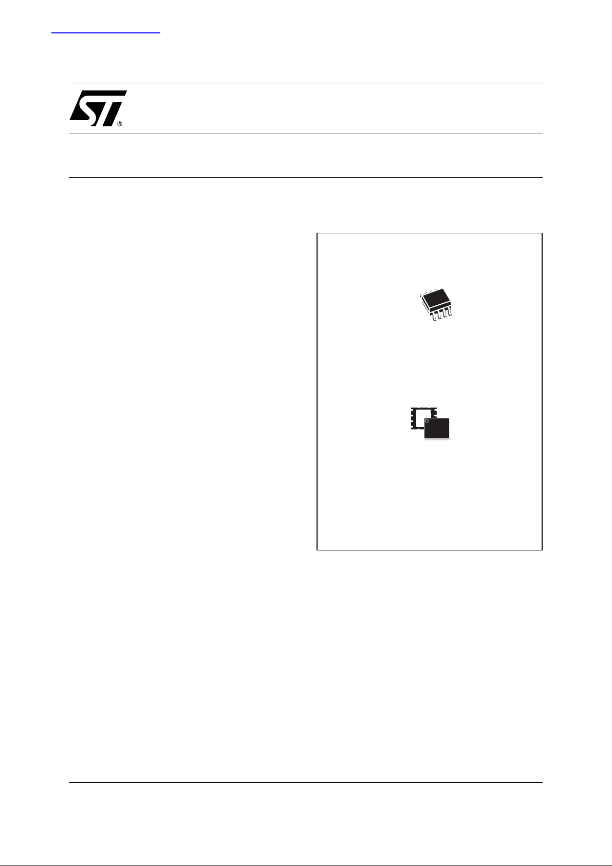
■ Packages
– ECOPACK® (RoHS compliant)
M45PE10
Figure 1. Packages
8
1
SO8 (MN)
150 mil width
VDFPN8 (MP)
(MLP8)
1/34October 2005

M45PE10
TABLE OF CONTENTS
FEATURES SUMMARY . . . . . . . . . . . . . . . . . . . . . . . . . . . . . . . . . . . . . . . . . . . . . . . . . . . . . . . . . . . . . 1
SUMMARY DESCRIPTION. . . . . . . . . . . . . . . . . . . . . . . . . . . . . . . . . . . . . . . . . . . . . . . . . . . . . . . . . . . 4
SIGNAL DESCRIPTION . . . . . . . . . . . . . . . . . . . . . . . . . . . . . . . . . . . . . . . . . . . . . . . . . . . . . . . . . . . . . 5
Serial Data Output (Q). . . . . . . . . . . . . . . . . . . . . . . . . . . . . . . . . . . . . . . . . . . . . . . . . . . . . . . . . . . . 5
Serial Data Input (D) . . . . . . . . . . . . . . . . . . . . . . . . . . . . . . . . . . . . . . . . . . . . . . . . . . . . . . . . . . . . . 5
Serial Clock (C) . . . . . . . . . . . . . . . . . . . . . . . . . . . . . . . . . . . . . . . . . . . . . . . . . . . . . . . . . . . . . . . . . 5
Chip Select (S) . . . . . . . . . . . . . . . . . . . . . . . . . . . . . . . . . . . . . . . . . . . . . . . . . . . . . . . . . . . . . . . . . 5
Reset (Reset
Write Protect (W). . . . . . . . . . . . . . . . . . . . . . . . . . . . . . . . . . . . . . . . . . . . . . . . . . . . . . . . . . . . . . . . 5
SPI MODES. . . . . . . . . . . . . . . . . . . . . . . . . . . . . . . . . . . . . . . . . . . . . . . . . . . . . . . . . . . . . . . . . . . . . . . 6
OPERATING FEATURES . . . . . . . . . . . . . . . . . . . . . . . . . . . . . . . . . . . . . . . . . . . . . . . . . . . . . . . . . . . . 7
Sharing the Overhead of Modifying Data . . . . . . . . . . . . . . . . . . . . . . . . . . . . . . . . . . . . . . . . . . . 7
An Easy Way to Modify Data . . . . . . . . . . . . . . . . . . . . . . . . . . . . . . . . . . . . . . . . . . . . . . . . . . . . . 7
A Fast Way to Modify Data . . . . . . . . . . . . . . . . . . . . . . . . . . . . . . . . . . . . . . . . . . . . . . . . . . . . . . . 7
Polling During a Write, Program or Erase Cycle . . . . . . . . . . . . . . . . . . . . . . . . . . . . . . . . . . . . . 7
Reset. . . . . . . . . . . . . . . . . . . . . . . . . . . . . . . . . . . . . . . . . . . . . . . . . . . . . . . . . . . . . . . . . . . . . . . . . 7
Active Power, Standby Power and Deep Power-Down Modes . . . . . . . . . . . . . . . . . . . . . . . . . . 7
Status Register . . . . . . . . . . . . . . . . . . . . . . . . . . . . . . . . . . . . . . . . . . . . . . . . . . . . . . . . . . . . . . . . 8
WIP bit. . . . . . . . . . . . . . . . . . . . . . . . . . . . . . . . . . . . . . . . . . . . . . . . . . . . . . . . . . . . . . . . . . . . . . . . 8
WEL bit . . . . . . . . . . . . . . . . . . . . . . . . . . . . . . . . . . . . . . . . . . . . . . . . . . . . . . . . . . . . . . . . . . . . . . . 8
Protection Modes . . . . . . . . . . . . . . . . . . . . . . . . . . . . . . . . . . . . . . . . . . . . . . . . . . . . . . . . . . . . . . 8
). . . . . . . . . . . . . . . . . . . . . . . . . . . . . . . . . . . . . . . . . . . . . . . . . . . . . . . . . . . . . . . . . . . 5
MEMORY ORGANIZATION . . . . . . . . . . . . . . . . . . . . . . . . . . . . . . . . . . . . . . . . . . . . . . . . . . . . . . . . . . 9
INSTRUCTIONS . . . . . . . . . . . . . . . . . . . . . . . . . . . . . . . . . . . . . . . . . . . . . . . . . . . . . . . . . . . . . . . . . . 10
Write Enable (WREN) . . . . . . . . . . . . . . . . . . . . . . . . . . . . . . . . . . . . . . . . . . . . . . . . . . . . . . . . . . 11
Write Disable (WRDI). . . . . . . . . . . . . . . . . . . . . . . . . . . . . . . . . . . . . . . . . . . . . . . . . . . . . . . . . . . 11
Read Identification (RDID) . . . . . . . . . . . . . . . . . . . . . . . . . . . . . . . . . . . . . . . . . . . . . . . . . . . . . . 12
Read Status Register (RDSR). . . . . . . . . . . . . . . . . . . . . . . . . . . . . . . . . . . . . . . . . . . . . . . . . . . . 13
WIP bit. . . . . . . . . . . . . . . . . . . . . . . . . . . . . . . . . . . . . . . . . . . . . . . . . . . . . . . . . . . . . . . . . . . . . . . 13
WEL bit . . . . . . . . . . . . . . . . . . . . . . . . . . . . . . . . . . . . . . . . . . . . . . . . . . . . . . . . . . . . . . . . . . . . . . 13
Read Data Bytes (READ). . . . . . . . . . . . . . . . . . . . . . . . . . . . . . . . . . . . . . . . . . . . . . . . . . . . . . . . 14
Read Data Bytes at Higher Speed (FAST_READ). . . . . . . . . . . . . . . . . . . . . . . . . . . . . . . . . . . . 15
Page Write (PW). . . . . . . . . . . . . . . . . . . . . . . . . . . . . . . . . . . . . . . . . . . . . . . . . . . . . . . . . . . . . . . 16
Page Program (PP) . . . . . . . . . . . . . . . . . . . . . . . . . . . . . . . . . . . . . . . . . . . . . . . . . . . . . . . . . . . . 17
Page Erase (PE). . . . . . . . . . . . . . . . . . . . . . . . . . . . . . . . . . . . . . . . . . . . . . . . . . . . . . . . . . . . . . . 18
Sector Erase (SE) . . . . . . . . . . . . . . . . . . . . . . . . . . . . . . . . . . . . . . . . . . . . . . . . . . . . . . . . . . . . . 19
Deep Power-down (DP) . . . . . . . . . . . . . . . . . . . . . . . . . . . . . . . . . . . . . . . . . . . . . . . . . . . . . . . . . 20
Release from Deep Power-down (RDP). . . . . . . . . . . . . . . . . . . . . . . . . . . . . . . . . . . . . . . . . . . . 21
2/34

M45PE10
POWER-UP AND POWER-DOWN . . . . . . . . . . . . . . . . . . . . . . . . . . . . . . . . . . . . . . . . . . . . . . . . . . . . 22
INITIAL DELIVERY STATE. . . . . . . . . . . . . . . . . . . . . . . . . . . . . . . . . . . . . . . . . . . . . . . . . . . . . . . . . . 23
MAXIMUM RATING. . . . . . . . . . . . . . . . . . . . . . . . . . . . . . . . . . . . . . . . . . . . . . . . . . . . . . . . . . . . . . . . 23
DC AND AC PARAMETERS. . . . . . . . . . . . . . . . . . . . . . . . . . . . . . . . . . . . . . . . . . . . . . . . . . . . . . . . . 24
PACKAGE MECHANICAL . . . . . . . . . . . . . . . . . . . . . . . . . . . . . . . . . . . . . . . . . . . . . . . . . . . . . . . . . . 30
PART NUMBERING . . . . . . . . . . . . . . . . . . . . . . . . . . . . . . . . . . . . . . . . . . . . . . . . . . . . . . . . . . . . . . . 32
REVISION HISTORY. . . . . . . . . . . . . . . . . . . . . . . . . . . . . . . . . . . . . . . . . . . . . . . . . . . . . . . . . . . . . . . 33
3/34
M45PE10
SUMMARY DESCRIPTION
The M45PE10 is a 1Mbit (128K x 8 bit) Serial
Paged Flash Memory accessed by a high speed
SPI-compatible bus.
The memory can be written or programmed 1 to
256 bytes at a time, using the Page Write or Page
Program instruction. The Page Write instruction
consists of an integrated Page Erase cycle followed by a Page Program cycle.
The memory is organized as 2 sectors, each containing 256 pages. Each page is 256 bytes wide.
Thus, the whole memory can be viewed as consisting of 512 pages, or 131,072 bytes.
The memory can be erased a page at a time, using
the Page Erase instruction, or a sect or at a time,
using the Sector Erase instruction.
In order to meet environmental requirements, ST
offers these devices in ECOPACK® packages.
ECOPACK® packages are Lead-free and RoHS
compliant.
ECOPACK is an ST trademark. ECOPACK specifications are available at: www.st.com.
Figure 2. Logic Diagram
V
CC
Figure 3. SO and VDFPN Connections
M45PE10
DQ
1
C
2
Reset
Note: 1. The re is an exposed d ie paddle on th e underside of th e
MLP8 package. This is pulled, internally, to VSS, and
must not be allowed to be connecte d to any oth er voltage
or signal line on the PCB.
2. See PACKAGE MECHANICAL section for packag e dimensions, and how to identify pin-1.
3
4
8
7
6
5
AI07404
V
SS
V
CC
WS
W
Reset
Table 1. Signal Names
D
C
S
M45PE10
V
SS
Q
AI07403
C Serial Clock
D Serial Data Input
Q Serial Data Output
S
Write Protect
W
Reset
Reset
V
CC
V
SS
Chip Select
Supply Voltage
Ground
4/34

SIGNAL DESCRIPTION
Serial Data Output (Q). This output signal is
used to transfer data serially out of the device.
Data is shifted out on the falling edge of Serial
Clock (C).
Serial Data Input (D). This input signal is used to
transfer data serially into the device. It receives instructions, addresses, and the data to be programmed. Values are latched on the risin g edge of
Serial Clock (C).
Serial Clock (C). This input signal provides the
timing of the serial interface. Instructions, addresses, or data present at Serial Data Input (D) are
latched on the rising edge of Serial Clock (C). Data
on Serial Data Output (Q) changes after the falling
edge of Serial Clock (C).
Chip Select (S
the device is deselected and Serial Data Output
(Q) is at high impedance. Unless an interna l Read,
Program, Erase or Write cycle is in progress, the
device will be in the Standby Power mode (this is
not the Deep Power-down mode). Driving Chip
Select (S
Active Power mode.
). When this input signal is High,
) Low selects the device, placing it in the
M45PE10
After Power-up, a falling edge on Chip Select (S
is required prior to the start of any instruction.
Reset (Reset
a hardware reset for the memory. In this mode, the
outputs are high impedance.
When Reset (Reset
in the normal operating mode. When Reset (Reset) is driven Low, the memory will enter the Reset
mode, provided that no internal operation is currently in progress. Driving Reset (Reset
an internal operation is in progress has no effect
on that internal operation (a write cycle, program
cycle, or erase cycle).
Write Protect (W
vice in the Hardware Protected mode, when Write
Protect (W
256 pages of memory to become read-o nly by protecting them from write, program and erase operations. When Write Protect (W
, the first 256 pages of memory behave like
V
CC
the other pages of memory.
). Th e Reset (Reset) input provides
) is driven High, the memory is
) Low while
). This input signal puts the de-
) is connected to VSS, causing the first
) is connected to
)
5/34
M45PE10
SPI MODES
These devices can be driven by a microcon troller
with its SPI peripheral running in either of the two
following modes:
– CPOL=0, CPHA=0
– CPOL=1, CPHA=1
For these two modes, input data is latched in on
the rising edge of Serial Clock (C), and output data
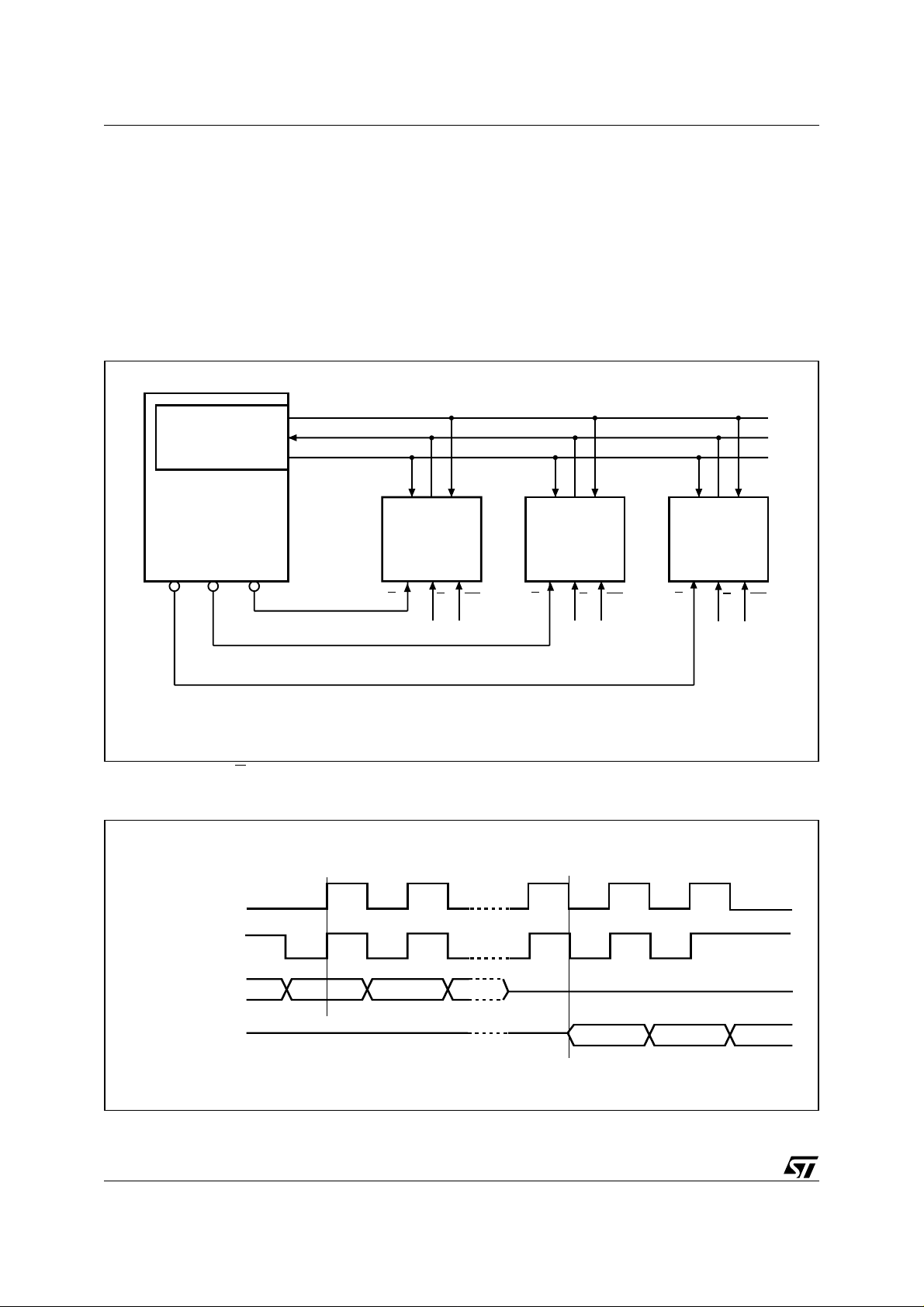
Figure 4. Bus Master and Memory Devices on the SPI Bus
is available from the falling edge of Serial Clock
(C).
The difference between the two modes, as shown
in Figure 5., is the clock polarity when the bus
master is in Stand-by mode and not transferring
data:
– C remains at 0 for (CPOL=0, CPHA=0)
– C remains at 1 for (CPOL=1, CPHA=1)
SPI Interface with
(CPOL, CPHA) =
(0, 0) or (1, 1)
Bus Master
(ST6, ST7, ST9,
ST10, Others)
CS3 CS2 CS1
Note: The Write Protect (W) signal should be driven, High or Low as appropriate.
SDO
SDI
SCK
CQD
SPI Memory
Device
S
RP
W
Figure 5. SPI Modes Supported
CQD
SPI Memory
Device
S
CQD
SPI Memory
Device
RP
W
S
W
AI04043B
RP
CPOL
6/34
CPHA
0
0
1
1
C
C
D
Q
MSB
MSB
AI01438B

OPERATING FEATURES
Sharing the Overhead of Modifying Data
To write or program one (or more) data bytes, two
instructions are required: Write Enable (WREN),
which is one byte, and a Page Write (PW) or Page
Program (PP) sequence, which consists of four
bytes plus data. This is followed by the internal cycle (of duration t
To share this overhead, the Page Write (PW) or
Page Program (PP) instruction allows up to 256
bytes to be programmed (changing bits from 1 to
0) or written (changing bits to 0 or 1) at a time, provided that they lie in consecutive addresses on the
same page of memory.
An Easy Way to Modify Data
The Page Write (PW) instruction provides a convenient way of modifying data (up to 256 contiguous bytes at a time), and simply requires the start
address, and the new data in the instruction sequence.
The Page Write (PW) instruction is entered by
driving Chip Select (S
the instruction byte, three address bytes (A23-A0)
and at least one data byte, and then driving Chip
Select (S
) High. While Chip Select (S) is being
held Low, the data bytes are written to the data
buffer, starting at the addr ess given in the third address byte (A7-A0). When Chip Select (S
High, the Write cycle starts. The remaining, unchanged, bytes of the data buffer are automatically
loaded with the values of the corresponding bytes
of the addressed memory page. The addressed
memory page then automatically put into an Erase
cycle. Finally, the addressed memory page is programmed with the contents of the data buffer.
All of this buffer management is handled internally,
and is transparent to the user. The user is given
the facility of being able to alter the contents of the
memory on a byte-by-byte basis.
For optimized timings, it is recommended to use
the Page Write (PW) instruction to write all consecutive targeted Bytes in a single sequence versus using several Page Write (PW) sequences
with each containing only a few Bytes (see Page
Write (PW) and AC Characteristics (33MHz operation)).
A Fast Way to Modify Data
The Page Program (PP) instruction provides a fast
way of modifying data (up to 256 contiguous byte s
at a time), provided that it only involves resetting
bits to 0 that had previously been set to 1.
This might be:
– when the designer is programming the device
for the first time
– when the designer knows that the page has
already been erased by an earlier Page Erase
or tPP).
PW
) Low, and then transmitting
) is driven
M45PE10
(PE) or Sector Erase (SE) instruction. This is
useful, for example, when storing a fast
stream of data, having first performed the
erase cycle when time was available
– when the designer knows that the only
changes involve resetting bits to 0 that are still
set to 1. When this method is possible, it has
the additional advantage of minimising the
number of unnecessary erase ope rations, and
the extra stress incurred by each page.
For optimized timings, it is recommended to use
the Page Program (PP) instruction to program all
consecutive targeted Bytes in a single sequence
versus using several Page Program (PP) sequences with each containing only a few Bytes
(see Page Program (PP) and AC Characteristics
(33MHz operation)).
Polling During a Write, Program or Eras e Cycle
A further improvement in the write, program or
erase time can be achieved by not waiting for the
worst case delay (t
In Progress (WIP) bit is provided in the Status
Register so that the application program can monitor its value, polling it to establish when the previous cycle is complete.
Reset
An internal Power On Reset circuit helps protect
against inadvertent data writes. Addition protection is provided by driving Reset (Reset
ing the Power-on process, and only driving it High
when V
V
CC
has reached the correct voltage level,
CC
(min).
Active Power, Standby Power and Deep
Power-Down Modes
When Chip Select (S
ed, and in the Active Power mode.
When Chip Select (S
lected, but could remain in the Active Power mode
until all internal cycles have completed (Program,
Erase, Write). The device then goes in to the
Standby Power mode. The device consumption
drops to I
CC1
.
The Deep Power-down mode is entered when the
specific instruction (the Deep Power-down (DP) instruction) is executed. The device consumption
drops further to I
mode until another specific instruction (the Release from Deep Power-down and Re ad Electro nic Signature (RES) instruction) is executed.
All other instructions are ignored while the device
is in the Deep Power-down mode. This can be
used as an extra software protection mechanism,
when the device is not in active use, to protect the
device from inadvertent Write, Program or Erase
instructions.
, tPP, tPE, or tSE). The Write
PW
) Low dur-
) is Low, the device is select-
) is High, the device is dese-
. The device remains in this
CC2
7/34
M45PE10
Status Register
The Status Register contains two status bits that
can be read by the Read Status Register (RDSR)
instruction.
WIP bit. The Write In Progress (WIP) bit indicates
whether the memory is busy with a Write, Progr am
or Erase cycle.
WEL bit. The Write Enable Latch (WEL) bit indicates the status of the internal Writ e Enable Latch.
Table 2. Status Register Format
b7 b0
0 0 0 0 0 0 WEL WIP
Note: WEL and WIP are volatile read-only bits (WEL is set and re-
set by specific instructions; WIP is automatically set and reset by the internal logic of the device).
Protection Modes
The environments where non-volatile memor y devices are used can be very noisy. No SPI device
can operate correctly in the presence of excessive
noise. To help combat this, the M45PE10 features
the following data protection mechanisms:
■ Power On Reset and an internal timer (t
PUW
can provide protection against inadvertant
changes while the power supply is outside the
operating specification.
■ Program, Erase and Write instructions are
checked that they consist of a number of clock
pulses that is a multiple of eight, before they
are accepted for execution.
■ All instructions that modify data must be
preceded by a Write Enable (WREN)
instruction to set the Write Enable Latch
(WEL) bit. This bit is returned to its reset state
by the following events:
– Power-up
– Reset (RESET
) driven Low
– Write Disable (WRDI) instruction
completion
– Page Write (PW) instruction completion
– Page Program (PP) instruction completion
– Page Erase (PE) instruction completion
– Sector Erase (SE) instruction completion
■ The Hardware Protected mode is entere d
when Write Protect (W
) is driven Low, causing
the first 256 pages of memory to become
read-only. When Write Protect (W
High, the first 256 pages of memory behave
like the other pages of memory
■ The Reset (Reset) signal can be driven Low to
)
protect the contents of the memory during any
critical time, not just during Power-up and
Power-down.
■ In addition to the low power consumption
feature, the Deep Power-down mode offers
extra software protection from inadvertant
Write, Program and Erase instructions while
the device is not in active use.
) is driven
8/34
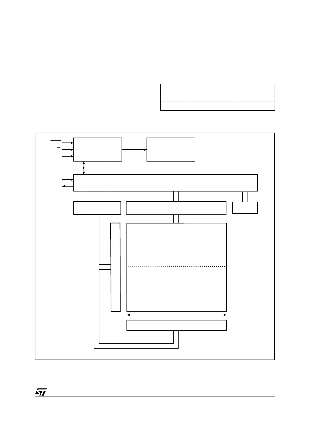
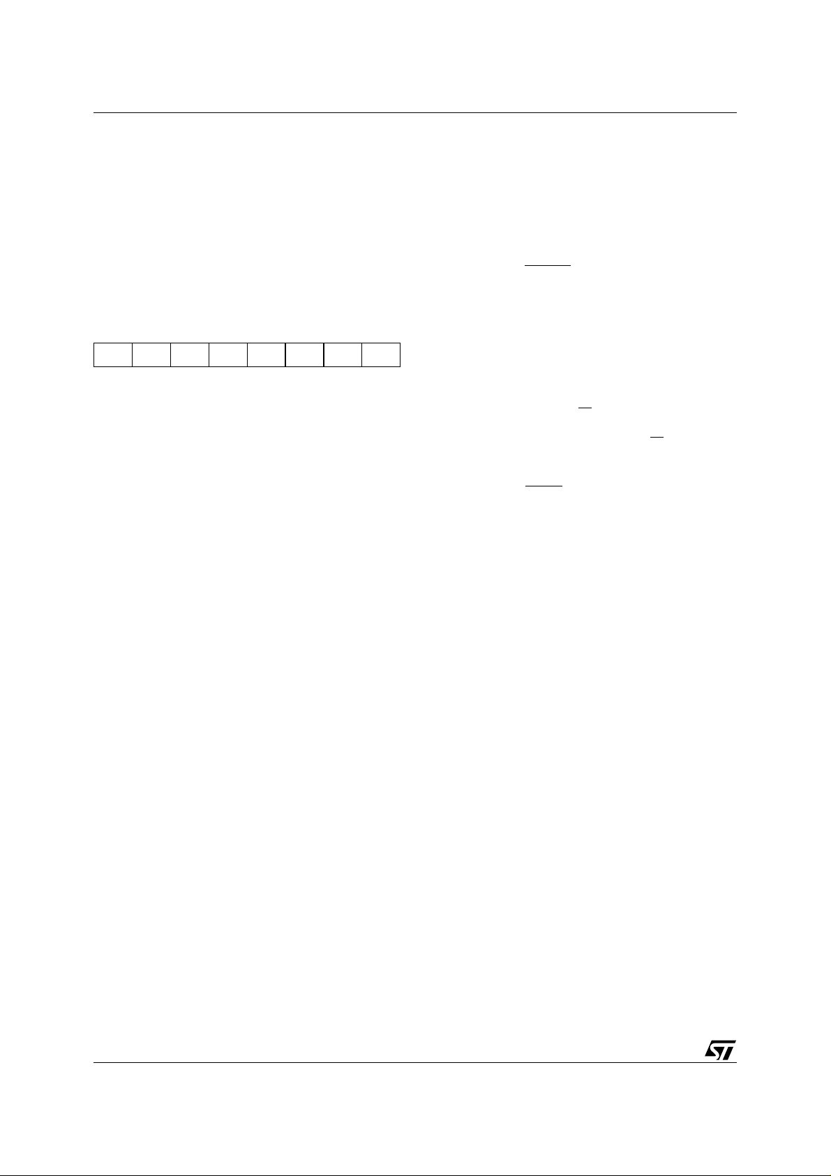
MEMORY ORGANIZATION
The memory is organized as:
■ 512 pages (256 bytes each).
■ 131,072 bytes (8 bits each)
■ 2 sectors (512 Kbits, 65536 bytes each)
Each page can be individually:
– programmed (bits are programmed from 1 to
0)
– erased (bits are erased from 0 to 1)
– written (bits are changed to either 0 or 1)
Figure 6. Block Diagram
M45PE10
The device is Page or Sector Erasable (bits ar e
erased from 0 to 1).
Table 3. Memory Organization
Sector Address Range
1 10000h 1FFFFh
0 00000h 0FFFFh
Reset
W
S
C
D
Q
Control Logic
Address Register
and Counter
10000h
Y Decoder
High Voltage
Generator
I/O Shift Register
256 Byte
Data Buffer
Status
Register
1FFFFh
First 256 Pages can
be made read-only
00000h
000FFh
256 Bytes (Page Size)
X Decoder
AI07405
9/34
M45PE10
INSTRUCTIONS
All instructions, addresses and data are shifted in
and out of the device, most significant bit firs t.
Serial Data Input (D) is sampled on the first rising
edge of Serial Clock (C) after Chip Select (S
) is
driven Low. Then, the one-byte instruction code
must be shifted in to the device, most significant bit
first, on Serial Data Input (D), each bit being
latched on the rising edges of Serial Clock (C).
The instruction set is listed in Table 4.
Every instruction sequence starts with a one-byte
instruction code. Depending on the instruction,
this might be followed by address bytes, or by data
bytes, or by both or none.
In the case of a Read Data Bytes (READ), Read
Data Bytes at Higher Speed (Fast_Read) or Read
Status Register (RDSR) instruction, the shifted-in
instruction sequence is followed by a data-out se-
quence. Chip Select (S
any bit of the data-out sequence is being shifted
out.
In the case of a Page Write (PW), Page Program
(PP), Page Erase (PE), Sector Erase (SE), Write
Enable (WREN), Write Disable (WRDI), Deep
Power-down (DP) or Release from Deep Pow erdown (RDP) instruction, Chip Select (S
driven High exactly at a byte boundary, otherwise
the instruction is rejected, and is not executed.
That is, Chip Select (S
number of clock pulses after Chip Select (S
driven Low is an exact multiple of eight.
All attempts to access the memory array during a
Write cycle, Program cycle or Erase cycle are ignored, and the internal Write cycle, Program cycle
or Erase cycle continues unaffected.
Table 4. Instruction Set
Instruction Description One-byte Instruction Code
WREN Write Enable 0000 0110 06h 0 0 0
WRDI Write Disable 0000 0100 04h 0 0 0
RDID Read Identification 1001 1111 9Fh 0 0 1 to 3
RDSR Read Status Register 0000 0101 05h 0 0 1 to ∞
READ Read Data Bytes 0000 0011 03h 3 0 1 to ∞
FAST_READ Read Data Bytes at Higher Speed 0000 1011 0Bh 3 1 1 to ∞
PW Page Write 0000 1010 0Ah 3 0 1 to 256
PP Page Program 0000 0010 02h 3 0 1 to 256
PE Page Erase 1101 1011 DBh 3 0 0
SE Sector Erase 1101 1000 D8h 3 0 0
DP Deep Power-down 1011 1001 B9h 0 0 0
RDP Release from Deep Power-down 1010 1011 ABh 0 0 0
) can be driven High after
) must be
) must driven High when the
) being
Address
Bytes
Dummy
Bytes
Data
Bytes
10/34
M45PE10
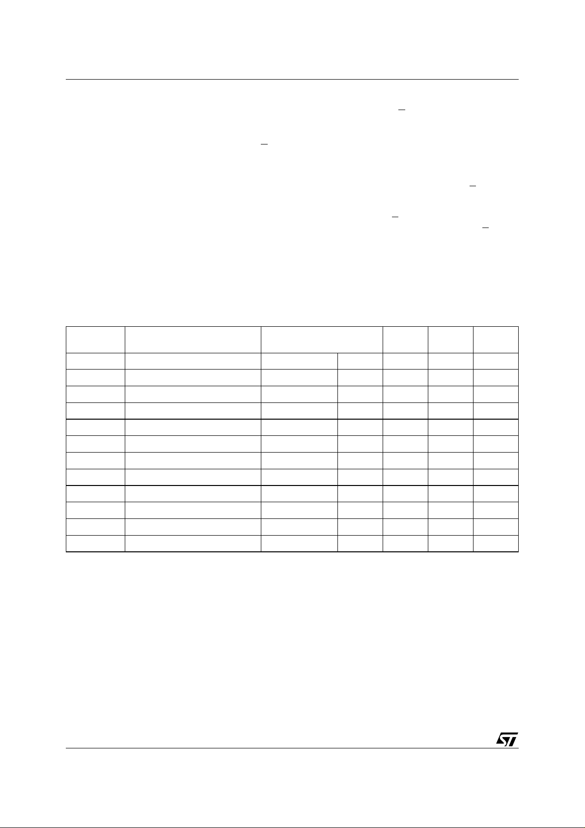
Write Enable (WREN)
The Write Enable (WREN) instruction (Figure 7.)
sets the Write Enable Latch (WEL) bit.
The Write Enable Latch (WEL) bit must be set pr ior to every Page Write (PW), Page Progr am (PP),
Page Erase (PE), and Sector Erase (SE) instruction.
The Write Enable (WREN) instruction is entered
by driving Chip Select (S
struction code, and then driving Chip Select (S
High.
Figure 7. Write Enable (WREN) Instruction Sequence
S
0
21 34567
C
Instruction
D
High Impedance
Q
Write Disable (WRDI)
The Write Disable (WRDI) instruction (Figure 8.)
resets the Write Enable Latch (WEL) bit.
The Write Disable (WRDI) instruction is entered by
driving Chip Select (S
tion code, and then driving Chip Select (S
) Low, sending the instruc-
) High.
The Write Enable Latch (WEL) bit is r eset under
–Power-up
– Write Disable (WRDI) instruction completion
– Page Write (PW) instruction comple tio n
– Page Program (PP) instruction completion
– Page Erase (PE) instruction completion
– Sector Erase (SE) instruction completion
the following conditions:
) Low, sending the in-
)
AI02281E
Figure 8. Write Disable (WRDI) Instruction Sequence
S
0
21 34567
C
Instruction
D
High Impedance
Q
AI03750D
11/34
M45PE10
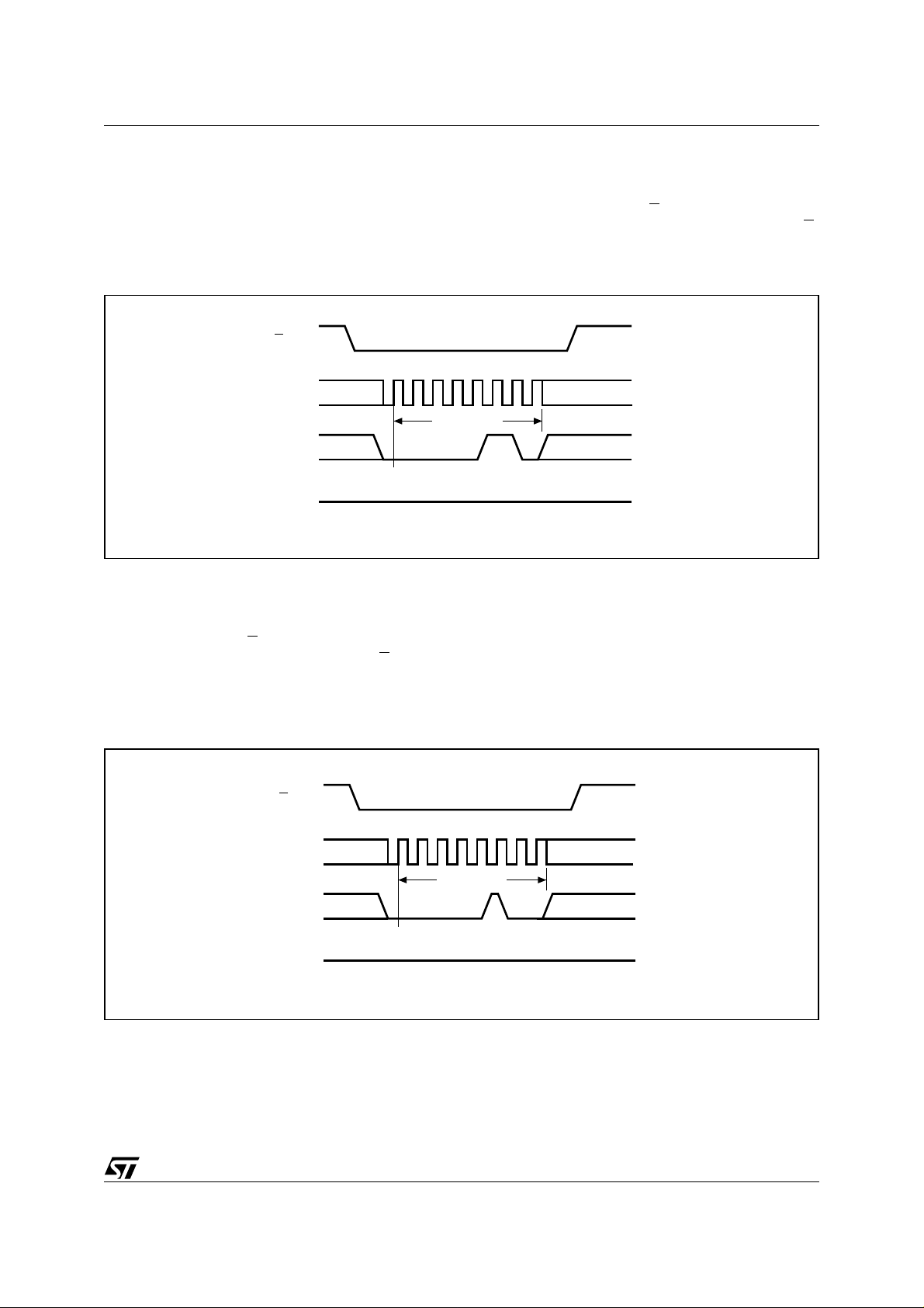
Read Identification (RDID)
The Read Identification (RDID) instruction allows
the 8-bit manufacturer identificat ion to be read, followed by two bytes of device identification. The
manufacturer identification is assigned by JEDEC,
and has the value 20h for STMicroelectronics. T he
device identification is assigned by the device
manufacturer, and indicates the memory type in
the first byte (40h), and the me mory capacity of the
device in the second byte (11h).
Any Read Identification (RDID) instruction while
an Erase or Program cycle is in progress, is not
decoded, and has no effect on the cycle that is in
progress.
struction is shifted in. This is followed by the 24-bit
device identification, stored in the memory, being
shifted out on Serial Data Output (Q), each bit being shifted out during the falling edge of Serial
Clock (C).
The instruction sequence is shown in Figure 9.
The Read Identification (RDID) instruction is termi-
nated by driving Chip Select (S
during data output.
When Chip Select (S
) is driven High, the device is
put in the Standby Power mode. Once in the
Standby Power mode, the device waits to be selected, so that it can receive, decode and execute
instructions.
The device is first selected by driving Chip Select
) Low. Then, the 8-bit instruct ion code f or the in-
(S
Table 5. Read Identification (RDID) Data- Out Sequence
Manufacturer Identification
Memory Type Memory Capacity
20h 40h 11h
Device Identification
Figure 9. Read Identification (RDID) Instruction Sequence and Data-Out Sequence
) High at any time
S
21 3456789101112131415
0
C
Instruction
D
Q
High Impedance
Manufacturer Identification
MSB
16 16 18 28 29 30 31
Device Identification
15 1413 3210
MSB
AI06809
12/34

M45PE10
Read Status Register (RDSR)
The Read Status Register (RDSR) instruction allows the Status Register to be read. The Status
Register may be read at any time, even while a
Program, Erase or Write cycle is in progress.
When one of these cycles is in progress, it is recommended to check the Write In Progress (WIP)
bit before sending a new instruction to the device.
It is also possible to read the Status Register continuously, as shown in Figure 10.
The status bits of the Status Register are as fol-
WIP bit. The Write In Progress (WIP) bit indicates
whether the memory is busy with a Write, Pr ogram
or Erase cycle. When set to 1, such a cycle is in
progress, when reset to 0 no such cycle is in
progress.
WEL bit. The Write Enable Latch (WEL) bit indicates the status of the internal Write Enable Lat ch.
When set to 1 the internal Write Enable Latch is
set, when set to 0 the internal Write Enable Latch
is reset and no Write, Program or Erase instruction
is accepted.
lows:
Figure 10. Read Status Register (RDSR) Instruction Sequence and Data-Out Sequence
S
21 3456789101112131415
0
C
Instruction
D
Q
High Impedance
Status Register Out
7 6543210
MSB
Status Register Out
7 6543210
MSB
7
AI02031E
13/34
M45PE10
Read Data Bytes (READ)
The device is first selected by driving Chip Select
) Low. The instruction code for the Read Data
(S
Bytes (READ) instruction is followed by a 3-byte
address (A23-A0), each bit being latched- in during
the rising edge of Serial Clock (C). Then the memory contents, at that address, is shifted out on Serial Data Output (Q), each bit being shifted out, at
a maximum frequency f
, during the falling edge of
R
Serial Clock (C).
The instruction sequence is shown in Figure 11.
The first byte addressed can be at any location.
The address is automatically incr emented to the
next higher address after each byte of data is sh ifted out. The whole memory can, ther efore, be read
with a single Read Data Bytes (READ) instruction.
When the highest address is reached, the a ddress
counter rolls over to 000000h, allowing the read
sequence to be continued indefinitely.
The Read Data Bytes (READ) instruction is terminated by driving Chip Select (S
) can be driven High at any time during data out-
(S
) High. Chip Select
put. Any Read Data Bytes (READ) instruction,
while an Erase, Program or Write cycle is in
progress, is rejected without having any effects on
the cycle that is in progress.
Figure 11. Read Data Bytes (READ) Instruction Sequence and Data-Out Sequence
S
21 345678910 2829303132333435
0
C
Instruction 24-Bit Address
36 37 38
39
D
High Impedance
Q
Note: Address bits A23 to A17 are Don’t Care.
23
2221 3210
MSB
Data Out 1
76543 1 7
MSB
2
0
Data Out 2
AI03748D
14/34

M45PE10
Read Data Bytes at Higher Speed
(FAST_READ)
The device is first selected by driving Chip Select
) Low. The instruction code for the Read Data
(S
Bytes at Higher Speed (FAST_READ) instruction
is followed by a 3-byte address (A23-A0) and a
dummy byte, each bit being la tched-in during the
rising edge of Serial Clock (C). Then the memory
contents, at that address, is shifted out on Serial
Data Output (Q), each bit being shifted out, at a
maximum frequency f
, during the falling edge of
C
Serial Clock (C).
The instruction sequence is shown in Figure 12.
The first byte addressed can be at any location.
The address is automatically incr emented to the
next higher address after each byte of data is sh ifted out. The whole memory can, ther efore, be read
with a single Read Data Bytes at Higher Speed
(FAST_READ) instruction. When the highest address is reached, the address counter rolls over to
000000h, allowing the read sequence to be co ntinued indefinitely.
The Read Data Bytes at Higher Speed
(FAST_READ) instruction is terminated by driving
Chip Select (S
) High. Chip Select (S) can be driven High at any time during data output. Any Read
Data Bytes at Higher Speed (FAST_READ) instruction, while an Erase, Program or Write cycle
is in progress, is rejected without having any effects on the cycle that is in progress.
Figure 12. Read Data Bytes at Higher Speed (FAST_READ) Instruction Sequence and Data-Out
Sequence
S
21 345678910 28293031
0
C
Instruction 24 BIT ADDRESS
D
High Impedance
Q
S
32 33 34 36 37 38 39 40 41 42 43 44 45 46
C
D
Q
Note: Address bits A23 to A17 are Don’t Care.
765432 0
35
Dummy Byte
23
2221 3210
1
DATA OUT 1
765432 0
MSB
47
DATA OUT 2
7 6543210
1
MSB MSB
7
AI04006
15/34
M45PE10
Page Write (PW)
The Page Write (PW) instruction allows bytes to
be written in the memory. Before it can be accept ed, a Write Enable (WREN) instruction must previously have been executed. After the Write Enable
(WREN) instruction has been decoded, the device
sets the Write Enable Latch (WEL).
The Page Write (PW) instruction is entered by
driving Chip Select (S
) Low, followed by the instruction code, three address bytes and at least
one data byte on Serial Data Input (D). The rest of
the page remains unchanged if no power failure
occurs during this write cycle.
The Page Write (PW) instruction performs a page
erase cycle even if only one byte is updated.
If the 8 least significant address bits (A7-A0) are
not all zero, all transmitted data exceeding the addressed page boundary wrap round, and are written from the start address of the same page (the
one whose 8 least significant address bits (A7- A0)
are all zero). Chip Select (S
) must be driven Low
for the entire duration of the sequence.
The instruction sequence is shown in Figure 13..
If more than 256 bytes are sent t o the device, pre-
viously latched data are discarded and the last 256
data bytes are guaranteed to be written correctly
within the same page. If less than 256 Data bytes
are sent to device, they are correctly writt en at t he
requested addresses without having any effects
on the other bytes of the same page.
For optimized timings, it is recommended to use
the Page Write (PW) instruction to write all consecutive targeted Bytes in a single sequence versus using several Page Write (PW) sequences
with each containing only a few Bytes (see AC
Characteristics (33MHz operation)).
Chip Select (S
) must be driven High after the
eighth bit of the last data byte has been latched in,
otherwise the Page Write (PW) instruction is not
executed.
As soon as Chip Select (S
timed Page Write cycle (whose duration is t
) is driven High, the self-
) is
PW
initiated. While the Page Write cycle is in progress,
the Status Register may be read to check the value of the Write In Progress (WIP) bit. The Wr ite In
Progress (WIP) bit is 1 during the self-timed Page
Write cycle, and is 0 when it is completed. At some
unspecified time before the cycle is co mplete, the
Write Enable Latch (WEL) bit is reset.
A Page Write (PW) instruction applied to a page
that is Hardware Protected is not executed.
Any Page Write (PW) instruction, while an Erase,
Program or Write cycle is in progress, is rejected
without having any effects on the cycle that is in
progress.
Figure 13. Page Write (PW) Instruction Sequence
S
21 345678910 2829303132333435
0
C
Instruction 24-Bit Address
23
D
S
4241 43 44 45 46 47 48 49 50 52 53 54 5540
C
Data Byte 2
D
Note: 1. Address bits A23 to A17 are Don’t Care
2. 1 ≤ n ≤ 256
765432 0
MSB MSB MSB
1
2221 3210
MSB
Data Byte 3 Data Byte n
765432 0
36 37 38
Data Byte 1
765432 0
MSB
51
1
765432 0
39
1
1
AI04045
16/34

M45PE10
Page Program (PP)
The Page Program (PP) instruction allows bytes to
be programmed in the memory (changing bits from
1 to 0, only). Before it can be accepted , a Write Enable (WREN) instruction must previously have
been executed. After the Write Enable (WREN) instruction has been decoded, the device sets the
Write Enable Latch (WEL).
The Page Program (PP) instruction is entered by
driving Chip Select (S
) Low, followed by the instruction code, three address bytes and at least
one data byte on Serial Data Input (D). If the 8
least significant address bits (A7-A0) are not all
zero, all transmitted data exceeding the addressed page boundary wrap round, and are programmed from the start address of the same page
(the one whose 8 least significant address bits
(A7-A0) are all zero). Chip Select (S
) must be driv-
en Low for the entire duration of the sequence.
The instruction sequence is shown in Figure 14..
If more than 256 bytes are sent t o the device, pre-
viously latched data are discarded and the last 256
data bytes are guaranteed to be programm ed correctly within the same page. If less than 256 Data
bytes are sent to device, they are correctly programmed at the requested addresses without having any effects on the other bytes of the same
page.
For optimized timings, it is recommended to use
the Page Program (PP) instruction to program all
consecutive targeted Bytes in a single sequence
versus using several Page Program (PP) sequences with each containing only a few Bytes
(see AC Characteristics (33MHz operation)).
Chip Select (S
) must be driven High after the
eighth bit of the last data byte has been latched in,
otherwise the Page Program (PP) instruction is not
executed.
As soon as Chip Select (S
timed Page Program cycle (whose duration is t
) is driven High, the self-
PP
is initiated. While the Page Program cycle is in
progress, the Status Register may be read to
check the value of the Write In Progress (WIP) bit .
The Write In Progress (WIP) bit is 1 duri ng the selftimed Page Program cycle, and is 0 when it is
completed. At some unspecified time before the
cycle is complete, the Write Enabl e Latch (WEL)
bit is reset.
A Page Program (PP) instruction applied to a page
that is Hardware Protected is not executed.
Any Page Program (PP) instruction, while an
Erase, Program or Write cycle is in progress, is rejected without having any effects on the cycle that
is in progress.
)
Figure 14. Page Program (PP) Instruction Sequence
S
21 345678910 2829303132333435
0
C
Instruction 24-Bit Address
23
D
S
4241 43 44 45 46 47 48 49 50 52 53 54 5540
C
Data Byte 2
D
Note: 1. Address bits A23 to A17 are Don’t Care
2. 1 ≤ n ≤ 256
765432 0
MSB MSB MSB
1
2221 3210
MSB
51
Data Byte 3 Data Byte n
765432 0
36 37 38
Data Byte 1
765432 0
MSB
1
765432 0
39
1
1
AI04044
17/34

M45PE10
Page Erase (PE)
The Page Erase (PE) instruction sets to 1 (F Fh) all
bits inside the chosen page. Before it can be accepted, a Write Enable (WREN) instruction must
previously have been executed. After the Write
Enable (WREN) instruction has been decoded,
the device sets the Write Enable Latch (WEL).
The Page Erase (PE) instruction is entered by
driving Chip Select (S
) Low, followed by the instruction code, and three address bytes on Serial
Data Input (D). Any address inside the Page is a
valid address for the Page Eras e (PE) in struc tion.
Chip Select (S
) must be driven Low for the entire
duration of the sequence.
The instruction sequence is shown in Figure 15..
Chip Select (S
) must be driven High after the
eighth bit of the last address byte has been latched
Figure 15. Page Erase (PE) Instruction Sequence
S
in, otherwise the Page Erase (PE) instruction is
not executed. As soon as Chip Select (S
) is driven
High, the self-timed Page Erase cycle (whose duration is t
) is initiated. While the Page Erase cy-
PE
cle is in progress, the Status Register may be r ead
to check the value of the Write In Progress (WIP)
bit. The Write In Progress (WIP) bit is 1 during the
self-timed Page Erase cycle, and is 0 when it is
completed. At some unspecified time before the
cycle is complete, the Write Enabl e Latch (WEL)
bit is reset.
A Page Erase (PE) instruction applied to a pag e
that is Hardware Protected is not executed.
Any Page Erase (PE) instruction, while an Erase,
Program or Write cycle is in progress, is rejected
without having any effects on the cycle that is in
progress.
0
C
D
Note: Address bits A23 to A17 are Don’t Care.
21 3456789 293031
Instruction
24 Bit Address
23 22 2 0
MSB
1
AI04046
18/34

M45PE10
Sector Erase (SE)
The Sector Erase (SE) instruction sets to 1 (FFh)
all bits inside the chosen sector. Before it can be
accepted, a Write Enable (WREN) instruction
must previously have been executed. After the
Write Enable (WREN) instruction has been decoded, the device sets the Write Enable Latch (WEL).
The Sector Erase (SE) instruction is entered by
driving Chip Select (S
) Low, followed by the instruction code, and three address bytes on Serial
Data Input (D). Any address inside the Sector ( see
Table 3.) is a valid address for the Sector Erase
(SE) instruction. Chip Select (S
) must be driven
Low for the entire duration of the sequence.
The instruction sequence is shown in Figure 16..
Chip Select (S
) must be driven High after the
eighth bit of the last address byte has been latched
in, otherwise the Sector Erase (SE) instruction is
Figure 16. Sector Erase (SE) Instruction Sequence
not executed. As soon as Chip Select (S
) is driven
High, the self-timed Sector Erase cycle (whose duration is t
) is initiated. While the Sector Erase cy-
SE
cle is in progress, the Status Register may be r ead
to check the value of the Write In Progress (WIP)
bit. The Write In Progress (WIP) bit is 1 during the
self-timed Sector Erase cycle, and is 0 when it is
completed. At some unspecified time before the
cycle is complete, the Write Enabl e Latch (WEL)
bit is reset.
A Sector Erase (SE) instruction applied to a sector
that contains a page that is Hardware Protected is
not executed.
Any Sector Erase (SE) instruction, while an Erase,
Program or Write cycle is in progress, is rejected
without having any effects on the cycle that is in
progress.
S
0
C
D
Note: Address bits A23 to A17 are Don’t Care.
21 3456789 293031
Instruction
24 Bit Address
23 22 2 0
MSB
1
AI03751D
19/34

M45PE10
Deep Power-down (DP)
Executing the Deep Power-down (DP) instruction
is the only way to put the device in the lowest consumption mode (the Deep Power- down mode). It
can also be used as an extra software protection
mechanism, while the device is not in act ive use,
since in this mode, the device ignores all Write,
Program and Erase instructions.
Driving Chip Select (S
) High deselects the device,
and puts the device in the Standby Power mode (if
there is no internal cycle currently in progress). But
this mode is not the Deep Powe r-down mode. The
Deep Power-down mode can only be entered by
executing the Deep Power-down (DP) instruction,
to reduce the standby current (from I
CC1
to I
CC2
as specified in Table 11.).
Once the device has entered the Deep Power-
down mode, all instructions are ignored except the
Release from Deep Power-down (RDP) instruction. This releases the device from this mod e.
The Deep Power-down mode automatically stops
at Power-down, and the device always Powers-up
in the Standby Power mode.
The Deep Power-down (DP) instruction is entered
by driving Chip Select (S
struction code on Serial Data Input (D). Chip Select (S
of the sequence.
The instruction sequence is shown in Figure 17..
Chip Select (S
eighth bit of the instruction code has been latched
in, otherwise the Deep Power-down (DP) instruction is not executed. As soon as Chip Select (S
driven High, it requires a delay of t
,
supply current is reduced to I
Power-down mode is entered.
Any Deep Power-down (DP) instruction, while an
Erase, Program or Write cycle is in progress, is rejected without having any effects on the cycle that
is in progress.
Figure 17. Deep Power-down (DP) Instruction Sequence
) Low, followed by the in-
) must be driven Low for the entire duration
) must be driven High after the
) is
before the
DP
and the Deep
CC2
S
t
21 345670
C
Instruction
D
DP
Stand-by Mode
Deep Power-down Mode
AI03753D
20/34

M45PE10
Release from Deep Power-down (RDP)
Once the device has entered the Deep Powerdown mode, all instructions are ignored except the
Release from Deep Power-down (RDP) instruction. Executing this instruction takes the device out
of the Deep Power-down mode.
The Release from Deep Power-down (RDP) instruction is entered by driving Chip Select (S
) Low,
followed by the instruction code on Serial Data Input (D). Chip Select (S
) must be driven Low for the
entire duration of the sequence.
The instruction sequence is shown in Figure 18..
The Release from Deep Power-down (RDP) in-
struction is terminated by driving Chip Select (S
High. Sending additional clock cycles on Serial
Clock (C), while Chip Select (S
cause the instruction to be rejected, and not executed.
After Chip Select (S
lowed by a delay, t
Standby Power mode. Chip Select (S
main High at least until this period is over. The device waits to be selected, so that it can receive,
decode and execute instructions.
Any Release from Deep Power-down (RDP) instruction, while an Erase, Program or Write cycle
is in progress, is rejected without having any effects on the cycle that is in progress.
)
Figure 18. Release from Deep Power-down (RDP) Instruction Sequence
S
t
21 345670
C
Instruction
RDP
) is driven Low,
) has been driven High, fol-
, the device is put in the
RDP
) must re-
D
High Impedance
Q
Deep Power-down Mode
Stand-by Mode
AI06807
21/34

M45PE10
POWER-UP AND POWER-DOWN
At Power-up and Power-down, the device must
not be selected (that is Chip Select (S
the voltage applied on V
) until VCC reaches the
CC
correct value:
–V
(min) at Power-up, and then for a further
CC
delay of t
VSL
–VSS at Power-down
Usually a simple pull-up resistor on Chip Select (S
can be used to ensure safe and proper Power-up
and Power-down.
To avoid data corruption and inadvertent write operations during power up, a Power On Reset
(POR) circuit is included. The logic inside the device is held reset while V
is less than the Power
CC
On Reset (POR) threshold value, V
tions are disabled, and the device does not respond to any instruction.
Moreover, the device ignores all Write Enable
(WREN), Page Write (PW), Page Program (PP),
Page Erase (PE) and Sector Erase (SE) instructions until a time delay of t
the moment that V
CC
PUW
rises above the VWI threshold. However, the correct operation of the device
is not guaranteed if, by this time, V
(min). No Write, Program or Erase instruct ions
V
CC
should be sent until the later of:
–t
after VCC passed the VWI threshold
PUW
) must follow
– all opera-
WI
has elapsed after
is still below
CC
–t
after wrap roundVCC passed the
VSL
(min) level
V
CC
These values are specified in Table 6..
If the delay, t
above V
CC
READ instructions even if the t
, has elapsed, after VCC has risen
VSL
(min), the device can be selected for
delay is not yet
PUW
fully elapsed.
)
As an extra protection, the Reset (Reset
can be driven Low for the whole duration of the
Power-up and Power-down phases.
At Power-up, the device is in the following state:
– The device is in the Standby Power mode (not
the Deep Power-down mode).
– The Write Enable Latch (WEL) bit is reset.
Normal precautions must be taken for supply rail
decoupling, to stabilize the V
vice in a system should have the V
supply. Each de-
CC
CC
pled by a suitable capacitor close to the package
pins. (Generally, this capacitor is of the order of
0.1µF).
At Power-down, when V
drops from the operat-
CC
ing voltage, to below the Power On Reset (POR)
threshold value, V
, all operations are disabled
WI
and the device does not respond to any instruction. (The designer needs to be aware that if a
Power-down occurs while a Write, Program or
Erase cycle is in progress, some data corrup tion
can result.)
) signal
rail decou-
Figure 19. Power-up Timing
V
CC
VCC(max)
Program, Erase and Write Commands are Rejected by the Device
Chip Selection Not Allowed
VCC(min)
Reset State
of the
V
Device
WI
tVSL
tPUW
Read Access allowed Device fully
accessible
time
AI04009C
22/34

M45PE10
Table 6. Power-Up Timing and VWI Threshold
Symbol Parameter Min. Max. Unit
1
t
VSL
t
PUW
V
Note: 1. These parameters are characterized only, over the temperature range –40°C to +85°C.
VCC(min) to S low
1
Time delay before the first Write, Program or Erase instruction 1 10 ms
1
Write Inhibit Voltage 1.5 2.5 V
WI
30 µs
INITIAL DELIVERY STATE
The device is delivered with the memory array
erased: all bits are set to 1 (each byte contains
FFh). All usable Status Register bits are 0.
MAXIMUM RATING
Stressing the device outside the ratings listed in
Table 7. may cause permanent damage to the de-
vice. These are stress ratings only, and operation
of the device at these, or any other conditions outside those indicated in the Oper ating sections of
this specification, is not implied. Exposure to Absolute Maximum Rating conditions for extended
periods may affect device reliability. Refer also to
the STMicroelectronics SURE Program and other
relevant quality documents.
Table 7. Absolute Maximum Ratings
Symbol Parameter Min. Max. Unit
T
STG
T
LEAD
V
IO
V
CC
V
ESD
Note: 1. Compliant with JEDEC Std J-STD-020B (for small body, Sn-Pb or Pb assembly), the ST ECOPACK® 7191395 specification, an d
the European directive on Restrictions on Hazardous Substances (RoHS) 2002/95/EU
2. JEDEC Std JESD22-A114A (C1=100 pF, R1=1500 Ω, R2=500 Ω)
Storage Temperature –65 150 °C
Lead Temperature during Soldering
See note
1
°C
Input and Output Voltage (with respect to Ground) –0.6 4.0 V
Supply Voltage –0.6 4.0 V
Electrostatic Discharge Voltage (Human Body model)
2
–2000 2000 V
23/34

M45PE10
DC AND AC PARAMETERS
This section summarizes the operating an d measurement conditions, and the DC and AC characteristics of the device. The parameters in the DC
and AC Characteristic tables that follow are derived from tests performed under the Measure-
Table 8. Operating Conditions
Symbol Parameter Min. Max. Unit
ment Conditions summarized in the relevant
tables. Designers should check that the operating
conditions in their circuit match the measurement
conditions when relying on the quoted parameters.
V
CC
T
A
Supply Voltage 2.7 3.6 V
Ambient Operating Temperature –40 85 °C
Table 9. AC Measurement Conditions
Symbol Parameter Min. Max. Unit
C
L
Load Capacitance 30 pF
Input Rise and Fall Times 5 ns
to 0.8V
Input Pulse Voltages
Input and Output Timing Reference Voltages
Note: Output Hi-Z is defined as the point where data out is no longer driven .
0.2V
0.3V
CC
to 0.7V
CC
CC
CC
Figure 20. AC Measurement I/O Waveform
Input Levels
0.8V
CC
0.2V
CC
Input and Output
Timing Reference Levels
0.7V
CC
0.3V
CC
AI00825B
V
V
Table 10. Capacitance
Symbol Parameter Test Condition Min. Max. Unit
C
OUT
C
IN
Note: Sampled only, not 100% tested, at TA=25°C and a frequency of 20 MHz.
24/34
Output Capacitance (Q) V
= 0V 8 pF
OUT
Input Capacitance (other pins) VIN = 0V 6 pF

Table 11. DC Characteristics
Symbol Parameter
I
Input Leakage Current ± 2 µA
LI
I
I
I
I
I
V
V
V
I
CC1
CC2
CC3
CC4
CC5
V
Output Leakage Current ± 2 µA
LO
Standby Current
(Standby and Reset modes)
Deep Power-down Current
Operating Current
(FAST_READ)
Operating Current (PW)
Operating Current (SE)
Input Low Voltage – 0.5
IL
Input High Voltage
IH
Output Low Voltage
OL
Output High Volta ge
OH
Test Condition
(in addition to those in Table 8.)
S
C = 0.1V
C = 0.1V
= VCC, V
S
= VCC, V
/ 0.9.VCC at 25MHz, Q = open
CC
/ 0.9.VCC at 33MHz, Q = open
CC
= VSS or V
IN
= VSS or V
IN
S
= V
CC
S
= V
CC
I
= 1.6 mA
OL
I
= –100 µAV
OH
CC
CC
M45PE10
Min. Max. Unit
50 µA
10 µA
6
8
15 mA
15 mA
0.3V
CC
0.7V
CC
CCVCC
–0.2
+0.4
0.4 V
mA
V
V
V
25/34

M45PE10
Table 12. AC Characteristics (25MHz operation)
Test conditions specified in Table 8. and Table 9.
Symbol Alt. Parameter Min. Typ. Max. Unit
f
C
f
R
1
t
CH
1
t
CL
t
SLCH
t
CHSL
t
DVCH
t
CHDX
t
CHSH
t
SHCH
t
SHSL
2
t
SHQZ
t
CLQV
t
CLQX
2
t
RLRH
t
RHSL
t
SHRH
t
WHSL
t
SHWL
2
t
DP
2
t
RDP
(3)
t
PW
(3)
t
PP
t
PE
t
SE
Note: 1. tCH + tCL must be greater than or equal to 1/ fC(max)
2. Value guaranteed by characterization, not 100% tested in production.
3. When using PP and PW instructions to update consecutive Bytes, optimized timings are obtained with one sequence including all
the Bytes versus several sequ ences of only a few Bytes. (1 ≤ n ≤ 256)
f
t
CLH
t
CLL
t
CSS
t
DSU
t
DH
t
CSH
t
DIS
t
t
HO
t
RST
t
REC
C
V
Clock Frequency for the following
instructions: FAST_READ, PW, PP, PE,
D.C. 25 MHz
SE, DP, RDP, WREN, WRDI, RDSR
Clock Frequency for READ instructions D.C. 20 MHz
Clock High Time 18 ns
Clock Low Time 18 ns
Clock Slew Rate
2
(peak to peak)
0.03 V/ns
S Active Setup Time (relative to C) 10 ns
S Not Active Hold Time (relative to C) 10 ns
Data In Setup Time 5 ns
Data In Hold Time 5 ns
S Active Hold Time (relative to C) 10 ns
S Not Active Setup Time (relative to C) 10 ns
S Deselect Time 200 ns
Output Disable Time 15 ns
Clock Low to Output Valid 15 ns
Output Hold Time 0 ns
Reset Pulse Width 10 µs
Reset Recovery Time 3 µs
Chip should have been deselected
before Reset is de-asserted
10 ns
Write Protect Setup Time 50 ns
Write Protect Hold Time 100 ns
S to Deep Power-down 3 µs
S High to Standby Pow er mode 30 µs
Page Write Cycle Time (256 Bytes) 11
Page Write Cycle Time (n Bytes)
10.2+
n*0.8/256
25 ms
Page Program Cycle Time (256 Bytes) 1.2
Page Program Cycle Time (n Bytes)
0.4+
n*0.8/256
5ms
Page Erase Cycle Time 10 20 ms
Sector Erase Cycle Time 1 5 s
26/34

M45PE10
Table 13. AC Characteristics (33MHz operation)
33MHz only available for products marked since week 40 of 2005
Test conditions specified in Table 8. and Table 9.
Symbol Alt. Parameter Min. Typ. Max. Unit
Clock Frequency for the following
f
C
f
C
instructions: FAST_READ, PW, PP,
PE, SE, DP, RDP, WREN, WRDI,
D.C. 33 MHz
RDSR
Clock Frequency for READ
instructions
D.C. 20 MHz
Clock High Time 13 ns
Clock Low Time 13 ns
Clock Slew Rate
2
(peak to peak)
0.03 V/ns
S Active Setup Time (relative to C) 10 ns
S Not Active Hold Time (relative to C) 10 ns
Data In Setup Time 3 ns
Data In Hold Time 5 n s
S Active Hold Time (relative to C) 5 ns
S Not Active Setup Time (relative to C) 5 ns
S Deselect Time 200 ns
Output Disable Time 12 ns
Clock Low to Output Valid 12 ns
Output Hold Time 0 ns
Top Sector Lock Setup Time 50 ns
Top Sector Lock Hold Time 100 ns
S to Deep Power-down 3 µs
S High to Standby Pow er mode 30 µs
t
CH
t
CL
t
SLCH
t
CHSL
t
DVCH
t
CHDX
t
CHSH
t
SHCH
t
SHSL
t
SHQZ
t
CLQV
t
CLQX
t
THSL
t
SHTL
t
DP
t
RDP
f
R
(1)
(1)
(2)
(2)
(2)
t
CLH
t
CLL
t
CSS
t
DSU
t
DH
t
CSH
t
DIS
t
t
HO
V
Page Write Cycle Time (256 Bytes) 11
(3)
t
PW
Page Write Cycle Time (n Bytes)
10.2+
n*0.8/256
Page Program Cycle Time (256 Bytes) 1.2
(3)
t
PP
t
PE
t
SE
Note: 1. tCH + tCL must be greater than or equal to 1/ f
2. Value guaranteed by characterization, not 100% tested in production.
3. When using PP and PW instructions to update consecutive Bytes, optimized timings are obtained with one sequence including all
the Bytes versus several sequ ences of only a few Bytes. (1 ≤ n ≤ 256)
4. Details of how to find the date of marking are given in Application Note, AN1995.
Page Program Cycle Time (n Bytes)
Page Erase Cycle Time 10 20 ms
Sector Erase Cycle Time 1 5 s
C
0.4+
n*0.8/256
(4)
25 ms
5ms
27/34

M45PE10
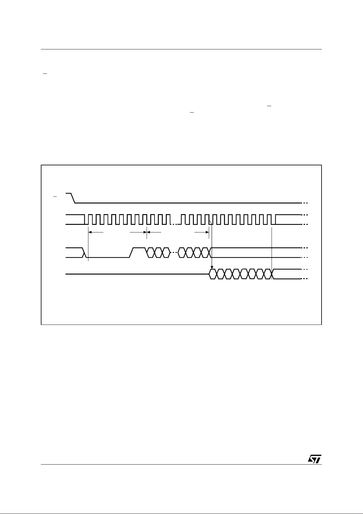
Figure 21. Serial Input Timing
S
C
tDVCH
tSLCH
tSHSL
tCHSHtCHSL
tSHCH
tCHCL
tCHDX
D
Q
MSB IN
High Impedance
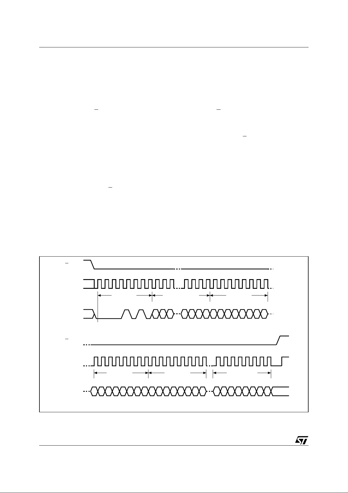
Figure 22. Write Protect Setup and Hold Timing
W
tWHSL
S
C
tCLCH
LSB IN
AI01447C
tSHWL
Q
28/34
D
High Impedance
AI07439

Figure 23. Output Timing
S
C
tCLQV
tCLQV
tCH
tCL
M45PE10
tSHQZ
tCLQX
Q
ADDR.LSB IN
D
tCLQX
Figure 24. Reset AC Waveforms
S
Reset
LSB OUT
tQLQH
tQHQL
AI01449D
tRHSLtSHRH
tRLRH
AI06808
29/34

M45PE10
PACKAGE MECHANICAL
Figure 25. SO8 narrow – 8 lead Plastic Small Outline, 150 mils body width, Package Outline
h x 45˚
Note: Drawing is not to scale.
B
SO-a
A
e
D
N
1
CP
E
H
C
LA1 α
Table 14. SO8 narrow – 8 lead Plastic Small Outline, 150 mils body width, Package Mechanical Data
Symb.
Typ. Min. Max. Typ. Min. Max.
A 1.35 1.75 0.053 0.069
A1 0.10 0.25 0.004 0.010
B 0.33 0.51 0.013 0.020
C 0.19 0.25 0.007 0.010
D 4.80 5.00 0.189 0.197
E 3.80 4.00 0.150 0.157
e1.27––0.050––
H 5.80 6.20 0.228 0.244
h 0.25 0.50 0.010 0.020
L 0.40 0.90 0.016 0.035
α 0° 8° 0° 8°
N8 8
CP 0.10 0.004
mm inches
30/34

Figure 26. MLP8, 8-lead Very thin Dual Flat Package No lead, 6x5mm, Package Outline
D
D1
E
E1
eE2
b
M45PE10
A
Note: Drawing is not to scale.
A1
θ
A2
A3
D2
L
VDFPN-01
Table 15. MLP8, 8-lead Very thin Dual Flat Package No lead, 6x5mm, Package Mechanical Da ta
Symb.
Typ. Min. Max. Typ. Min. Max.
A 0.85 1.00 0.0335 0.0394
A1 0.00 0.05 0.0000 0.0020
A2 0.65 0.0256
A3 0.20 0.0079
b 0.40 0.35 0.48 0.0157 0.0138 0.0189
D 6.00 0.2362
D1 5.75 0.2264
D2 3.40 3.20 3.60 0.1339 0.1260 0.1417
E 5.00 0 .1969
E1 4.75 0.1870
E2 4.00 3.80 4.20 0.1575 0.1496 0.1654
e 1.27 0.0500
L 0.60 0.50 0.75 0.0236 0.0197 0.0295
θ 12° 12°
mm inches
31/34

M45PE10
PART NUMBERING
Table 16. Ordering Information Scheme
Example: M 45PE10 – V MP 6 T G
Device T ype
M45PE = Serial Flash Memory for Data Storage
Device Function
10 = 1Mbit (128K x 8)
Operating Voltage
V = V
Package
MN = SO8 (150 mil width)
MP = VDFPN8 6x5mm (MLP8)
Device Grade
6 = Industrial temperature range, –40 to 85 °C.
Device tested with standard test flow
= 2.7 to 3.6V
CC
Option
blank = Standard Packing
T = Tape and Reel Packing
Plating Technology
blank = Standard SnPb plating
P or G = ECOPACK® (RoHS compliant)
For a list of available options (speed, package,
etc.) or for further information on any aspect of this
device, please contact your nearest ST Sales Office.
The category of second Level Interconnect is
marked on the package and on the inner box label,
in compliance with JEDEC Standard JESD97. The
maximum ratings related to soldering conditions
are also marked on the inner box label.
32/34

REVISION HISTORY
Table 17. Document Revision History
Date Version Description of Revision
29-Apr-2003 1.0 Document written
04-Jun-2003 1.1
04-Dec-2003 1.2
25-Jun-2004 1.3
22-Sep-2004 2.0 Document promoted to Preliminary Data. Minor wording changes
08-Oct-2004 3.0 Document promoted to Mature Datasheet. No other changes
4-Oct-2005 4.0
Description corrected of entering Hardware Protected mode (W
cannot be left unconnected).
V
(min) extended to –0.6V, tPW(typ) and tPP(typ) improved. Table of contents, warning
IO
about exposed paddle on MLP8, and Pb-free options added. Change of naming for
VDFPN8 package.
Soldering temperature information clarified for RoHS compliant devices. De vice Grade
clarified.
Added AC Characteristics (33MHz operation). An Easy Way to Modify Data, A Fast
Way to Modify Data, Page Write (PW) and Page Program (PP) sections updated to
explain optimal use of Page Write and Page Program instructions. Updated I
values in Table 11., DC Characteristics. Updated Table 16., Ordering Information
Scheme. Added Ecopack® information.
M45PE10
must be driven, and
CC3
33/34

M45PE10
Information furnished is believe d to be accura te and re liable. Howev er, STMi croelec tronics assumes n o resp onsibil ity for t he consequences
of use of such information nor f or any infringement of pa tents or other rights of third parties which may re sult from its use. N o license is granted
by implication or otherwise und er an y pa ten t or patent rights of STMicroelectronics. Specifications mentioned in thi s p ub lic ation are subject
to change without notice. This publication supersedes and replaces all information previously supplied. STMicroelectronics products are not
authorized for use as critical components in life support devices or systems without express written approval of STMicroelectronics.
The ST logo is a registered trademark of STMicroelectronics.
All other names are the property of their respective owners
© 2005 STMicroelectronics - All rights reserved
Australia - Belgium - Brazil - Canada - China - Czech Republic - Finland - France - Germany - Hong Kong - India - Israel - Italy - Japan -
Malaysia - Malta - Morocco - Singapore - Spain - Sweden - Switzerland - United Kingdom - United States of America
STMicroelectronics group of companies
www.st.com
34/34
 Loading...