

查询M41T80供应商
FEATURES SUMMARY
■ 2.0 TO 5.5V CLOCK OPERATING VOLTA GE
■ COUNTERS FOR TENTHS/HUNDREDTHS
OF SECONDS, SECONDS, MINUTES,
HOURS, DAY, DATE, MONT H , YEAR , and
CENTURY
■ SERIAL INTERFAC E SU PPO R TS I
(400KHz)
■ PROGRAMMABLE ALARM and INTERRUP T
FUNCTI ON
■ LOW OPERATING CURRENT OF 200µA
■ OPERATING TEMPERATURE OF –40 TO
85°C
2
M41T80
SERIAL ACCESS RTC WITH ALARMS
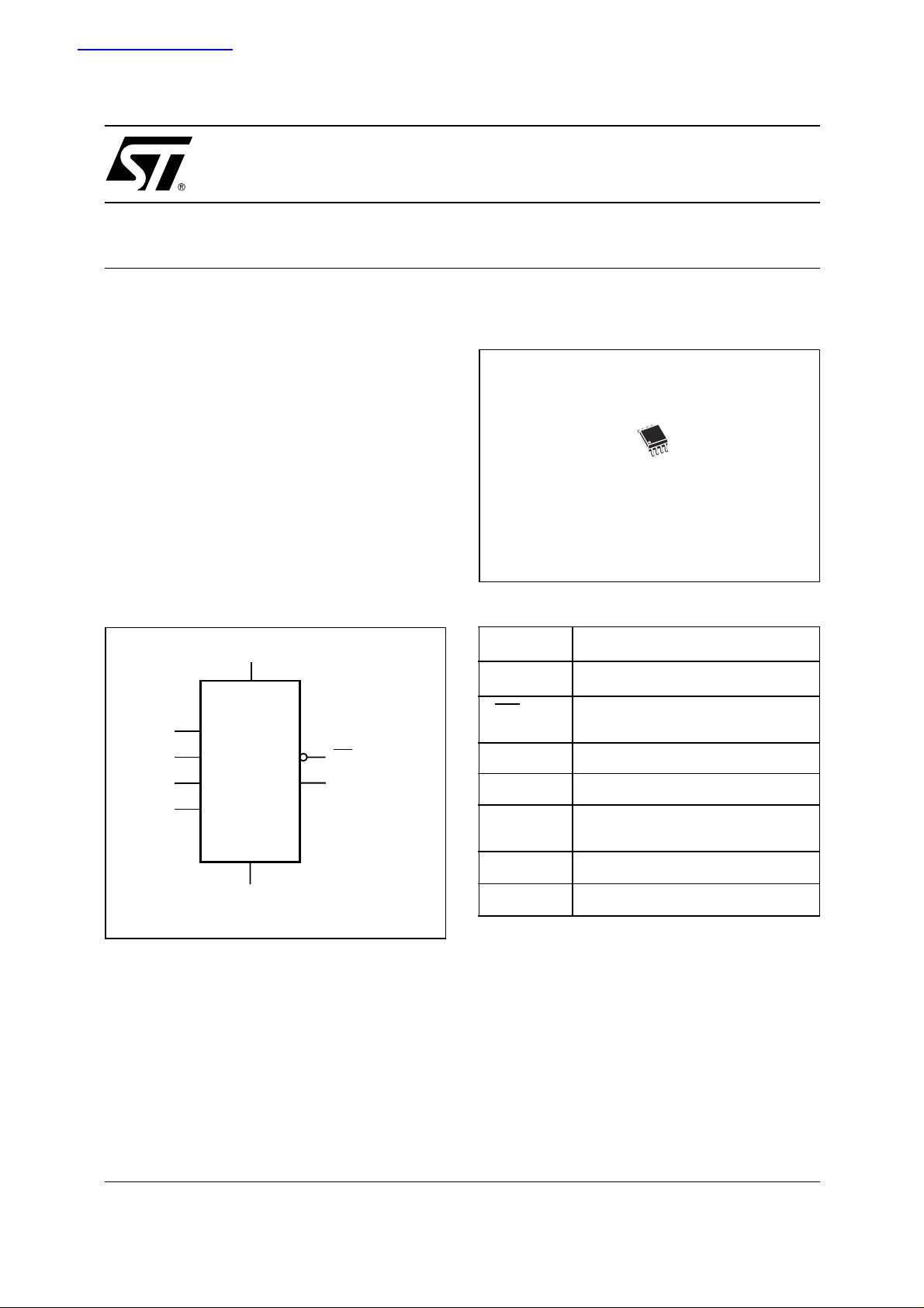
Figure 2. 8-pi n S OI C Package
C BUS
8
1
SO8 (M)
Figure 1. Logic Diagram
V
CC
XI
XO
SCL
SDA
M41T80
V
SS
IRQ/OUT/SQW
F
32k
AI07005
Table 1. Signal Names
XI
XO
IRQ
/OUT/
SQW
SDA Serial Data Input/Output
SCL Serial Clock Input
F
32k
V
CC
V
SS
Oscillator Input
Oscillator Output
Interrupt / Output Driver / Square
Wave (Open Drain)
32kHz Square Wave Output (Open
drain)
Supply Voltage
Ground
1/20October 2002

M41T80
TABLE OF CONTENTS
SUMMARY DESCRIPTION. . . . . . . . . . . . . . . . . . . . . . . . . . . . . . . . . . . . . . . . . . . . . . . . . . . . . . . . . . . 3
8-pin SOIC Connections (Figure 3.) . . . . . . . . . . . . . . . . . . . . . . . . . . . . . . . . . . . . . . . . . . . . . . . . . 3
Block Diagram (Fi g ure 4 .) . . . . . . . . . . . . . . . . . . . . . . . . . . . . . . . . . . . . . . . . . . . . . . . . . . . . . . . . . 3
MAXIMUM RATING. . . . . . . . . . . . . . . . . . . . . . . . . . . . . . . . . . . . . . . . . . . . . . . . . . . . . . . . . . . . . . . . . 4
Absolute Maximum Rati ng s (Table 2.) . . . . . . . . . . . . . . . . . . . . . . . . . . . . . . . . . . . . . . . . . . . . . . .4
DC AND AC PARAMETERS. . . . . . . . . . . . . . . . . . . . . . . . . . . . . . . . . . . . . . . . . . . . . . . . . . . . . . . . . . 5
Operating and AC Measurement Conditions (Table 3.) . . . . . . . . . . . . . . . . . . . . . . . . . . . . . . . . . . 5
AC Measurement I/O Waveform (Figure 5.) . . . . . . . . . . . . . . . . . . . . . . . . . . . . . . . . . . . . . . . . . . . 5
Capacitance (Table 4.) . . . . . . . . . . . . . . . . . . . . . . . . . . . . . . . . . . . . . . . . . . . . . . . . . . . . . . . . . . . 5
DC Characteristi cs (Table 5.) . . . . . . . . . . . . . . . . . . . . . . . . . . . . . . . . . . . . . . . . . . . . . . . . . . . . . . 6
Crystal Electrical Characteristics (Table 6.). . . . . . . . . . . . . . . . . . . . . . . . . . . . . . . . . . . . . . . . . . . . 6
OPERATION . . . . . . . . . . . . . . . . . . . . . . . . . . . . . . . . . . . . . . . . . . . . . . . . . . . . . . . . . . . . . . . . . . . . . . 7
2-Wire Bus Characteristics . . . . . . . . . . . . . . . . . . . . . . . . . . . . . . . . . . . . . . . . . . . . . . . . . . . . . . . . 7
Serial Bus Data Transfer Sequence (Figure 6.) . . . . . . . . . . . . . . . . . . . . . . . . . . . . . . . . . . . . . . . .8
Acknowledgement Sequ ence (Figure 7.) . . . . . . . . . . . . . . . . . . . . . . . . . . . . . . . . . . . . . . . . . . . . . 8
Bus Timing Requirements Sequence (Figure 8.) . . . . . . . . . . . . . . . . . . . . . . . . . . . . . . . . . . . . . . . 9
AC Characteristics (Table 7.) . . . . . . . . . . . . . . . . . . . . . . . . . . . . . . . . . . . . . . . . . . . . . . . . . . . . . . 9
READ Mode. . . . . . . . . . . . . . . . . . . . . . . . . . . . . . . . . . . . . . . . . . . . . . . . . . . . . . . . . . . . . . . . . . . 1 0
Slave Address Location (Figure 9.). . . . . . . . . . . . . . . . . . . . . . . . . . . . . . . . . . . . . . . . . . . . . . . . . 10
READ Mode Sequence (Figure 10.) . . . . . . . . . . . . . . . . . . . . . . . . . . . . . . . . . . . . . . . . . . . . . . . . 10
Alternative READ Mode Sequence (Figure 11.) . . . . . . . . . . . . . . . . . . . . . . . . . . . . . . . . . . . . . . .11
WRITE Mode. . . . . . . . . . . . . . . . . . . . . . . . . . . . . . . . . . . . . . . . . . . . . . . . . . . . . . . . . . . . . . . . . . 11
WRITE Mode Sequence (Figure 12.) . . . . . . . . . . . . . . . . . . . . . . . . . . . . . . . . . . . . . . . . . . . . . . . 11
CLOCK OPERATION . . . . . . . . . . . . . . . . . . . . . . . . . . . . . . . . . . . . . . . . . . . . . . . . . . . . . . . . . . . . . . 12
TIMEKEEPER® Registers. . . . . . . . . . . . . . . . . . . . . . . . . . . . . . . . . . . . . . . . . . . . . . . . . . . . . . . . 12
TIMEKEEPER® Register Map (Table 8.) . . . . . . . . . . . . . . . . . . . . . . . . . . . . . . . . . . . . . . . . . . . . 13
Full-time 32kHz Square Wave Output . . . . . . . . . . . . . . . . . . . . . . . . . . . . . . . . . . . . . . . . . . . . . . .15
Century Bit. . . . . . . . . . . . . . . . . . . . . . . . . . . . . . . . . . . . . . . . . . . . . . . . . . . . . . . . . . . . . . . . . . . . 16
Alarm Interrupt Reset Waveform (Figure 13.) . . . . . . . . . . . . . . . . . . . . . . . . . . . . . . . . . . . . . . . . . 14
Alarm Repeat Modes (Table 9.) . . . . . . . . . . . . . . . . . . . . . . . . . . . . . . . . . . . . . . . . . . . . . . . . . . . 14
Square Wave Output Frequency (Table 10.). . . . . . . . . . . . . . . . . . . . . . . . . . . . . . . . . . . . . . . . . . 15
Century Bit. . . . . . . . . . . . . . . . . . . . . . . . . . . . . . . . . . . . . . . . . . . . . . . . . . . . . . . . . . . . . . . . . . . . 16
Output Driver Pin. . . . . . . . . . . . . . . . . . . . . . . . . . . . . . . . . . . . . . . . . . . . . . . . . . . . . . . . . . . . . . . 16
Preferred Power-on Def a ult. . . . . . . . . . . . . . . . . . . . . . . . . . . . . . . . . . . . . . . . . . . . . . . . . . . . . . . 16
Preferred Power-on Def a ult Values (Table 11.) . . . . . . . . . . . . . . . . . . . . . . . . . . . . . . . . . . . . . . . 16
PART NUMBERING . . . . . . . . . . . . . . . . . . . . . . . . . . . . . . . . . . . . . . . . . . . . . . . . . . . . . . . . . . . . . . . 17
PACKAGE MECHANICAL INFORMATION . . . . . . . . . . . . . . . . . . . . . . . . . . . . . . . . . . . . . . . . . . . . . 18
REVISION HISTORY. . . . . . . . . . . . . . . . . . . . . . . . . . . . . . . . . . . . . . . . . . . . . . . . . . . . . . . . . . . . . . . 19
2/20
M41T80
SUMMARY DESCRIPTION
The M41T80 Serial Access TIMEKEEPER
SRAM is a low power Serial RTC with a built-in
32.768 KHz oscillator (external crystal controlled).
Eight registers (see Table 8, page 13) are used for
the clock/calendar func tion and a re configured in
binary coded decimal (BCD) format. An additional
12 registers provide status/control of Alarm, 32kHz
output, and Square Wave functions. Addresses
and data are transferred se rially via a t wo li ne, bidirectional I
2
C interface. The built-in address register is incremented automatically after each
WRITE or READ data byte.
Figure 3. 8-pin SOIC Connections
V
1
XI
2
XO
(1)
F
32k
V
SS
Note: 1. Open drain output.
M41T80
3
45
8
CC
7
IRQ/OUT/SQW
6
SCL
SDA
(1)
AI07006
®
Functions available to the user include a time-ofday clock/calendar, Alarm interrup ts, 32kHz output, and programmable Square Wave output. The
eight clock address locations contain the cent ury,
year, month, date, day, hour, minute, second and
tenths/hundredths of a second in 24 hour BCD format. Corrections for 28, 29 (leap yea r - valid until
year 2100), 30 and 31 day months are made automatically.
The M41T80 is supplied in an 8-pin SOIC.
Figure 4. Block Diagram
CRYSTAL
SDA
SCL
Note: 1. Open Drain output
32KHz
OSCILLATOR
I2C
INTERFACE
REAL TIME CLOCK
CALENDAR
RTC W/ALARM
SQUARE WAVE
AF
IRQ/OUT/SQW
(1)
F
32k
AI07007
(1)
3/20
M41T80
MAXIMUM RATIN G
Stressing the device above the rating l isted in the
“Absolute Maximum Ratings” table may cause
permanent damage to the device. These are
stress ratings only and operation of the dev ice at
these or any other conditions above those indicated in the Operating sections of this specification is
Table 2. Absolute Maximum Ratings
Sym Parameter Value Unit
T
STG
V
CC
T
SLD
V
IO
I
O
P
Note: 1. Reflow at peak temperature of 215°C to 225°C for < 60 sec onds (total thermal budg et not to exce ed 180°C for bet ween 90 to 12 0
Storage Temperature (VCC Off, Oscillator Off)
Supply Voltage –0.3 to 7 V
(1)
Lead Solder Temperature for 10 Seconds 260 °C
Input or Output Voltages –0.3 to Vcc+0.3 V
Output Current 20 mA
Power Dissipation 1 W
D
secon ds).
not implied. Exposure to Absol ute Maxim um Rating conditions for extended periods may affect device reliability. Refer also to the
STMicroelectronics SURE Program and oth er relevant quality documents.
–55 to 125
°C
4/20
DC AND AC PARAMETERS
This section summarizes the operat ing and measurement conditions, as well as the DC and AC
characteristics of the device. The parameters in
the following DC and AC Characteristic tables are
derived from tests performed under the M easure-
Table 3. Operating and AC Measurement Conditions
Parameter M41T80
M41T80
ment Conditions listed i n the relevant tables. Designers should check that the operating conditions
in their projects match the measurement conditions when using the quoted parameters.
Supply Voltage (V
Ambient Operating Temperature (T
Load Capacitance (C
CC
)
)
A
)
L
2.0 to 5.5V
–40 to 85°C
100pF
Input Rise and Fall Times ≤ 50ns
0.2V
0.3V
to 0.8 V
CC
to 0.7 V
CC
Input Pulse Voltages
Input and Output Timing Ref. Voltages
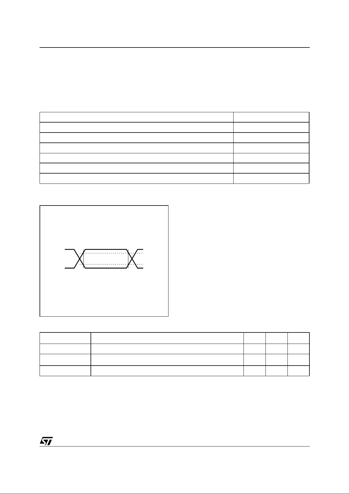
Note: Output Hi -Z is define d as the point wh ere data is no longer driven.
Figure 5. AC Measurement I/O Waveform
0.8V
0.2V
CC
CC
0.7V
0.3V
AI02568
CC
CC
CC
CC
Table 4. Capacitance
Symbol
C
IN
(3)
C
OUT
t
LP
Note: 1. Effective capacitance measured with power suppl y at 5V; sampled only, not 100% tested.
2. At 25°C, f = 1MHz.
3. Outputs deselected .
Input Capacitance 7 pF
Output Capacitance 10 pF
Low-pass filter input time constant (SDA and SCL) 50 ns
Parameter
(1,2)
Min Max Unit
5/20
M41T80
Table 5. DC Characteristics
Symbol Parameter
Input Leakage
I
LI
Current
Output Leakage
I
LO
Current
I
CC2
I
Supply Current Switch Freq (SCL) = 400kHz
CC1
Supply Current
(2)
(standby)
V
Input Low Voltage –0.3
IL
V
Input High Voltage
IH
All Inputs = V
Switch Freq (SCL) = 0Hz
Output Low Voltage
V
OL
Output Low Voltage
(Open Drain)
Note: 1. Valid for Am bi ent Operat in g T em perature : TA = –40 to 85°C ; VCC = 2.0 to 5.5V (except where noted).
2. At 25°C.
3. For IRQ
/FT/OUT, RST, and 32kHz pins (Open Drain)
(3)
Test Condition
0V ≤ V
0V ≤ V
OUT
– 0.2V
CC
I
= 3.0mA 0.4
OL
IOL = 10mA
(1)
≤ V
IN
CC
≤ V
CC
32KE = 1
or SQWE = 1
32KE = 0
and SQWE = 0
Min Typ Max Unit
3.0V 30 µA
5.5V 200 µA
3.0V 1.8 3.0 µA
5.5V 35 µA
3.0V 1.5 2.4 µA
5.5V 31 µA
0.7V
CC
±1 µA
±1 µA
0.3V
CC
VCC + 0.3
0.4 V
V
V
V
Table 6. Crystal Electrical Characteristics
Sym
f
O
R
S
C
L
Note: 1. Externally s uppl ied i f us ing th e S O8 pa ckag e. STM icroe lec troni cs reco mm ends the K DS DT -38: 1TA/ 1TC 252E 127, Tun ing Fork
Type (thru-hole) or the DMX-26S: 1TJS125FH2A212, (SMD) quartz crystal for industrial temperature operations. KDS can be contacted at kouhou@kdsj .c o.jp or http ://www.kds j .c o.jp for further inform at i on on this crystal type.
2. Load capacitors are integrated within the M41T80. Circuit board layout considerations for the 32.768 kHz crystal of minimum trace
lengths an d i solation from RF generating signals should be taken into account.
Resonant Frequency 32.768 kHz
Series Resistance 60 kΩ
Load Capacitance 12.5 pF
Parameter
(1,2)
Min Typ Max Units
6/20

OPERATION
The M41T80 clock operates as a slave device on
the serial bus. Access is obtained by implementing
a start condition followed by the correct slav e address (D0h). The 20 bytes contained in the device
can then be accessed sequentially in the following
order:
1. Tenths/Hundredths of a Second Register
2. Seconds Register
3. Minutes Register
4. Century/Hours Register
5. Day Register
6. Date Register
7. Month Register
8. Year Register
9. Control Register
10. 32kE Bit
11 - 16. Alarm Registers
17 - 19. Reserved
20 - Square Wave Register
2-Wire Bus Characteristics
The bus is intended for communication between
different IC’s. It consists of two lines: a bi-directional data signal (SDA) and a clock signal (SCL).
Both the SDA and SCL lines must be connected to
a positive supply voltage via a pull-up resistor.
The following protocol has been defined:
– Data transfer may be initiated only when the bus
is not busy.
– During data trans fer, the dat a line mus t remain
stable whenever the clock line is High.
– Changes in the data line, while the clock line is
High, will be interpreted as control signals.
Accordingly, the following bus conditions have
been defined:
Bus not busy. Both data and clock lines remain
High.
M41T80
Start data transfer. A c hange in the st ate of the
data line, from high to Low, while the clock is High,
defines the START condition.
Stop data transfer. A change in the state of the
data line, from Low to High, whil e the c lock is Hi gh,
defines the STOP condition.
Data Valid. The state of the data line represents
valid data when after a start condition, the data line
is stable for the duration of the high period of the
clock signal. The data on the line may be changed
during the Low period of the clock signal. There is
one clock pulse per bit of data.
Each data transfer is initiated with a start condition
and terminated with a stop condition. The number
of data bytes transferred between the start and
stop conditions is not limited. The information is
transmitted byte-wide and each receiver acknowledges with a ninth bit.
By definition a device that gives o ut a m essag e is
called “transmitter,” the receiving device that gets
the message is called “receiver.” The device that
controls the message is called “master.” The devices that are controlled by the master are cal led
“slaves.”
Acknowledge. Eac h byte of eight bits is followed
by one Acknowledge Bit. This Acknowledge Bit is
a low level put on the bus by the receiver whereas
the master generates an extra acknowledge related clock pulse. A slave receiver which is addressed is obliged to generate an acknowledge
after the reception of each byte that has been
clocked out of the slave transmitter.
The device that acknowledges has to pull down
the SDA line during the acknowledge clock pulse
in such a way that the SDA line is a stable Low during the High period of the acknowledge related
clock pulse. Of course, setup and hold times must
be taken into account. A master receiver must signal an end of data to the slave transm itter by not
generating an acknowledge on the last byte that
has been clocked out of the slave. In this case the
transmitter must leave the data line High to enable
the master to generate the STOP condition.
7/20

M41T80
Figure 6. Serial Bus Data Transfer Sequence
DATA LINE
STABLE
DATA VALID
CLOCK
DATA
START
CONDITION
Figure 7. Acknowledgement Sequence
START
SCL FROM
MASTER
DATA OUTPUT
BY TRANSMITTER
DATA OUTPUT
BY RECEIVER
12 89
MSB LSB
CHANGE OF
DATA ALLOWED
STOP
CONDITION
AI00587
CLOCK PULSE FOR
ACKNOWLEDGEMENT
AI00601
8/20

Figure 8. Bus Timing Requirements Sequence
SDA
M41T80
tHD:STA
SCL
tHD:STAtBUF
tR
SP
tHIGH
tLOW
tF
tSU:DAT
tHD:DAT
SR
Table 7. AC Characteristics
Sym
f
SCL
t
LOW
t
HIGH
t
R
t
F
t
HD:STA
t
SU:STA
t
SU:DAT
t
HD:DAT
t
SU:STO
t
BUF
Note: 1. Valid for Am bi ent Operat in g T em perature : TA = –40 to 85°C ; VCC = 2.0 to 5.5V (except where noted).
2. Transmitter must in ternally p rov i de a hold time to bridge the undefined region (300ns max) of the falling edge of SC L.
SCL Clock Frequency 0 400 kHz
Clock Low Period 1.3 µs
Clock High Period 600 ns
SDA and SCL Rise Time 300 ns
SDA and SCL Fall Time 300 ns
START Condition Hold Time
(after this period the first clock pulse is generated)
START Condition Setup Time
(only relevant for a repeated start condition)
(2)
Data Setup Time 100 ns
Data Hold Time 0 µs
STOP Condition Setup Time 600 ns
Time the bus must be free before a new
transmission can start
Parameter
(1)
Min Typ Max Units
600 ns
600 ns
1.3 µs
tSU:STOtSU:STA
P
AI00589
9/20

M41T80
READ Mode
In this mode the master reads the M41T80 slave
after setting the slave address (see Figure 10,
page 10). Following the WRITE Mode Control Bit
=0) and the Acknowledge Bit, the word ad-
(R/W
dress 'An' is written to the on-chip address pointer.
Next the START condition and slave address are
repeated followed by the RE AD Mode Control Bit
(R/W
=1). At this point the master transmitter becomes the master receiver. The data byte which
was addressed will be trans mi tted and t he master
receiver will send an Acknowledge Bit to the slave
transmitter. The address pointer is only incremented on reception of an Acknowledge Clock. The
M41T80 s lave tr ansmitt er will now place the data
byte at address An+1 on the bus, the master receiver reads and acknowledges the n ew byte and
the address pointer is incremented to “An+2.”
Figure 9. Slave Address Location
This cycle of reading con secutive addresses will
continue until the mast er receiver sends a STOP
condition to the slave transmitter.
The system-to-user transfer of clock data will be
halted whenever the address being read is a clock
address (00h to 07h). The update will resume due
to a Stop Condition or when the pointer increments
to any non-clock address (08h-13h).
Note: This is true both in READ Mode and WRITE
Mode.
An alternate READ Mode may also be implemented whereby the master reads the M41T80 slave
without first writing to the (volatile) a ddress pointer. The first address that is read is the last one
stored in the pointer (see Figure 11, page 11).
R/W
START A
Figure 10. READ Mode Sequence
BUS ACTIVITY:
MASTER
SDA LINE
BUS ACTIVITY:
START
S
ADDRESS
R/W
ACK
SLAVE
MSB
WORD
ADDRESS (An)
STOP
SLAVE ADDRESS
0100011
START
S
ACK
SLAVE
ADDRESS
LSB
AI00602
R/W
DATA n DATA n+1
ACK
ACK
ACK
10/20
DATA n+X
P
AI00899
NO ACK

Figure 11. Alternative READ Mode Sequence
M41T80
BUS ACTIVITY:
MASTER
BUS ACTIVITY:
START
S
SLAVE
ADDRESS
R/W
DATA n DATA n+1 DATA n+X
ACK
WRITE Mode
In this mode the master transmitter transmits to
the M41T80 slave receiver. Bus protocol is shown
in Figure 12, page 11. Following the ST ART condition and slave address, a logic '0' (R/W
=0) is
placed on the bus and indicates to the addressed
device t ha t w or d address “ An” will follow an d is to
be written to the on-chip address pointer. The data
word to be written to the memory is strobed in next
Figure 12. WRITE Mode S equence
BUS ACTIVITY:
MASTER
START
R/W
STOP
PSDA LINE
ACK
ACK
ACK
NO ACK
AI00895
and the internal address pointer is incremented to
the next address location on the reception of an
acknowledge clock. The M41T80 slave receiver
will send an acknowledge clock to the master
transmitter after it has received t he sla ve addres s
see Figure 9, page 1 0 and again after it has received the word address and each data byte.
STOP
BUS ACTIVITY:
S
ADDRESS
SLAVE
WORD
ADDRESS (An)
ACK
DATA n DATA n+1 DATA n+X
ACK
ACK
ACK
PSDA LINE
ACK
AI00591
11/20

M41T80
CLOCK OPERATION
The M41T80 is driven by a quartz-controlled oscillator with a nominal frequency of 32,768Hz. The
accuracy of the Real Time Clock depends on the
frequency of the quartz crystal that i s used as the
time-base for the RTC.
The 20-byte Register Map (see Table 8, pa ge 13)
is used to both set the clock and to read t he date
and time from the clock, in a binary coded decimal
format. Tenths/Hundredths of S econds, Seconds,
Minutes, and Hours are contained within the f irst
four registers.
Note: A WRIT E to any cloc k reg is ter w ill resu lt in
the Tenths/Hundredths of Seconds bei ng reset to
“00,” and Tenths/Hundredths of Seconds cannot
be written to any value other than “00.”
Bits D6 and D7 of Clock Register 03h (Century/
Hours Register) contain the CENTURY ENABLE
Bit (CEB) and the CENTURY Bit (CB). Setting
CEB to a '1' will cause CB to toggle, either from '0'
to '1' or from '1' to '0' at the turn of the century (depending upon its initial state). If CEB is set to a '0,'
CB will not toggle. Bits D0 through D2 of Regi ster
04h contain the Day (day of week). Registers 05h,
06h, and 07h contain the Date (day of month),
Month and Years. The ninth clock register is the
Control Register. Bit D7 of Register 01h contains
the STOP Bit (ST). Setting this bit to a '1' will cause
the oscillator to stop. If the device is expected to
spend a significant amount of time on the shelf, the
oscillator may be stopped to reduce current drain.
When reset to a '0' the oscillator restarts within
four seconds (typically one second).
The eight Clock Registers may be read one byte at
a time, or in a sequential block. Provision has been
made to assure that a clock update does not occur
while any of the eight clock addresses are being
read. If a clock address is being read, an update of
the clock registers will be halted. T his will prevent
a transition of data during the READ.
®
TIMEKEEPER
Registers
The M41T80 offers 20 internal registers which
contain Clock, Alarm, 32kHz, Flag, Square Wave,
and Control data. These registers are memory locations which contain external (user accessible)
and internal copies of the data (usually referred to
as BiPORT
™
TIMEKEEPER cells). The external
copies are independent of internal functions except that they are updated periodically by the simultaneous transfer of the incremented internal
copy. The internal divider (or clock) chain will be
reset upon the completion of a WRITE to any clock
address.
The system-to-user transfer of clock data will be
halted whenever the address being read is a clock
address (00h to 07h). The update will resum e either due to a Stop Condition or when the pointer
increments to any non-clock address (08h-13h).
TIMEKEEPER and Alarm Registers store data in
BCD. Control, 32kHz, and Square Wave Registers
store data in Binary Format.
12/20

M41T80
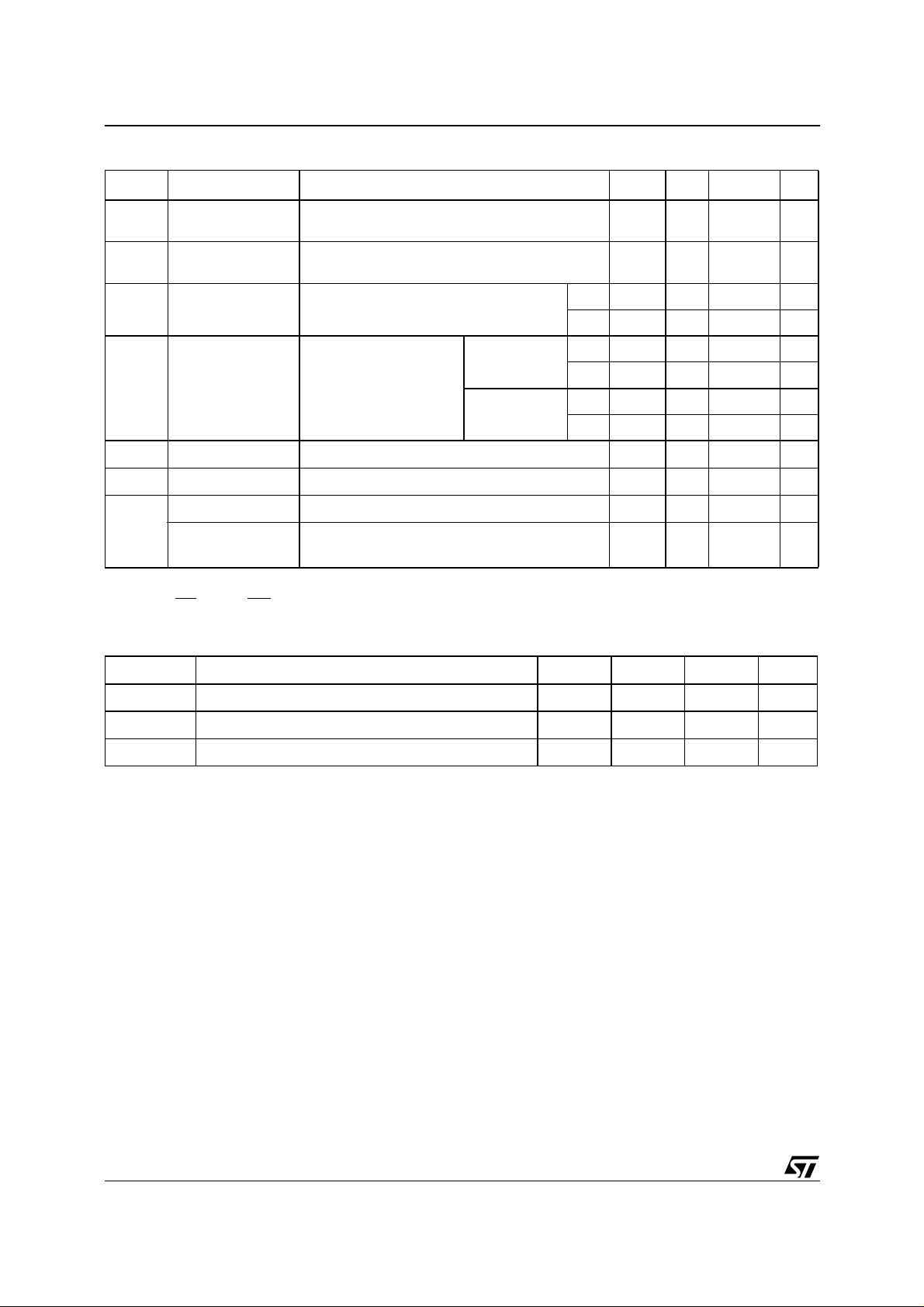
Table 8. TIMEKEEPER® Register M ap
Addr
D7 D6 D5 D4 D3 D2 D1 D0
00h 0.1 Seconds 0.01 Seconds
01h ST 10 Seconds Seconds Seconds 00-59
02h 0 10 Minutes Minutes Minutes 00-59
Function/Range BCD
Format
10s/100s
of Seconds
00-99
03h CEB CB 10 Hours Hours (24 Hour Format)
Century/
Hours
0-1/00-23
04h 0 0 0 0 0 Day of Week Day 01-7
05h 0 0 10 Date Date: Day of Month Date 01-31
06h 0 0 0 10M Month Month 01-12
07h 10 Years Year Year 00-99
08h OUT 0 0 0
0000Control
09h 32kE 0 0 0 0 0 0 0 32kHz
0Ah AFE SQWE 0 Al 10M Alarm Month Al Month 01-12
0Bh RPT4 RPT5 AI 10 Date Alarm Date Al Date 01-31
0Ch RPT3 0 AI 10 Hour Alarm Hour Al Hour 00-23
0Dh RPT2 Alarm 10 Minutes Alarm Minutes Al Min 00-59
0Eh RPT1 Alarm 10 Seconds Alarm Seconds Al Sec 00-59
0Fh 0 AF 0 0 0 0 0 0 Flags
10h 0 0 0 0 0 0 0 0 Reserved
11h 0 0 0 0 0 0 0 0 Reserved
12h 0 0 0 0 0 0 0 0 Reserved
13h RS3 RS2 RS1 RS0 0 0 0 0 SQW
Keys: ST = Stop Bit
0 = Must be set to '0'
32kE = 32kHz Enable Bit
CEB = Centur y E nable Bit
CB = Centur y B i t
OUT = Output level
AFE = Alarm Flag Enable Flag
RPT1-RPT5 = Alarm Repeat Mode Bits
AF = Alarm Flag (Read only)
SQWE = Square Wave Enable
RS0-RS3 = SQW Frequency
13/20

M41T80
Setting Alarm Clock Registers
Address locations 0Ah-0Eh contain the alarm settings. The alarm can be configured to go off at a
prescribed time on a specific month, date, hour,
minute, or second or repeat every year, month,
day, hour, minute, or second.
Bits RPT5-RPT1 put the alarm in the repeat mode
of operation. Table 9, page 14 shows the possible
configurations. Codes not listed in the table default
to the once per second mode to quickly alert the
user of an incorrect alarm setting.
When the clock information matches the alarm
clock settings based on the m atch criteria d efi ned
by RPT5-RPT1, the AF (Alarm Flag) is set. If AFE
(Alarm Flag Enable) is also set (and SQWE is '0.'),
Figure 13. Alarm Interrupt Reset Waveform
ACTIVE FLAG
the alarm condition activates the I RQ
/OUT/SQW
pin.
Note: If the address pointer is allowed to incre-
ment to the Flag Register address, an alarm condition will not cause the Interrupt/Flag to occur until
the address pointer is moved to a different address. It should also be noted that if the last address written is the “Alarm Seconds,” the address
pointer will increment to the Flag address, causing
this situation to occur.
The IRQ
/OUT/SQW output is cl eared by a READ
to the Flags Register as shown in Figure 13. A
subsequent READ of the Flags Register is necessary to see that the value of the Alarm Flag has
been reset to '0.'
0Fh0Eh 10h
IRQ/OUT/SQW
Table 9. Alarm Repeat Modes
RPT5 RPT4 RPT3 RPT2 RPT1 Alarm Setting
1 1 1 1 1 Once per Second
1 1 1 1 0 Once per Minute
1 1 1 0 0 Once per Hour
1 1 0 0 0 Once per Day
1 0 0 0 0 Once per Month
0 0 0 0 0 Once per Year
HIGH-Z
AI07021
14/20

Table 10. Square Wave Output Frequency
Square Wave Bits Square Wave
RS3 RS2 RS1 RS0 Frequency Units
0000None0 0 0 1 32.768 kHz
0 0 1 0 8.192 kHz
0 0 1 1 4.096 kHz
0 1 0 0 2.048 kHz
0 1 0 1 1.024 kHz
0110512Hz
0111256Hz
1000128Hz
100164Hz
101032Hz
101116Hz
11008Hz
11014Hz
M41T80
11102Hz
11111Hz
Full-time 32kHz Square Wave Output
The M41T80 offers the user a special 32kHz
square wave function which defaults to output on
the F
pin (Pin 3) as long as VCC is valid, and the
32k
oscillator is running (ST Bit = '0'). This function is
available within four seconds of initial power-up
and can only be disabled by setting the 32kE Bit to
'0' or the ST Bit to '1.' If not used, the F
should be disconnected and allowed to float.
Note: The F
pin is an open drain which requires
32k
an external pull-up resistor.
32k
pin
15/20

M41T80
Century Bit
Bits D7 and D6 of Clock Register 03h contain the
CENTURY ENABLE Bit (CEB) and the CENTURY
Bit (CB). Setting CEB to a '1' will cause CB to toggle, either from a '0' to '1' or from '1' to '0' at the turn
of the century (depending upon its initial state). If
CEB is set to a '0,' CB will not toggle.
Output Driver Pin
When the AFE Bit and S QWE Bit are not s et, the
/OUT/SQW pin becomes an output driver that
IRQ
reflects the contents of D7 of the Control Register.
In other words, when D7 (OUT Bit) of address lo-
Table 11. Preferred Power-on Default Values
Condition ST Out AFE SQWE 32kE
Power-up
Note: 1. If VCC falls to a voltage, 0V < VCC < 2.0V, these b its should be rew ri t ten by the user.
(1)
01001
cation 08h is a '0,' then the IRQ
be driven low.
Note: The IRQ
which requires an external pull-up resistor.
Preferred Power-on Default
When powering the device up from ground (0V),
the following register bits are set to a '0' state: ST;
AFE; and SQWE. The following bits are set to a '1'
state: OUT and 32kE (see Table 11, page 16).
/OUT/SQW pin will
/OUT/SQW pin is an open drain
16/20

M41T80
PART NUMBERING
Table 12. Ordering Information Scheme
Example: M41T 80 M 6 TR
Device Type
M41T
Supply Voltage and Write Protect Voltage
80 = V
Package
M = SO8
Temperature Rang e
6 = –40°C to 85°C
= 2.0 to 5.5V
CC
Shipping Method for SOIC
blank = Tubes
TR = Tape & Reel
For a list of available options (e.g., Speed, Package) or for further information on any aspect of this device,
please contact the ST Sales Office nearest to you.
17/20

M41T80
PACKAGE MECHANICAL INFORMATION
Figure 14. SO8 – 8 lead Plastic Small Outline, 150 mils body width, Package Mechanical Drawing
h x 45˚
A2
A
C
B
e
ddd
D
8
E
H
1
Note: Drawing is not to scale.
LA1 α
SO-A
Table 13. SO8 – 8-lead Plastic Small Outline, 150 mils body width, Package Mechanical Data
Symb
T yp Min Max T yp Min Max
mm inches
A – 1.35 1.75 – 0.053 0.069
A1 – 0.10 0.25 – 0.004 0.010
B – 0.33 0.51 – 0.013 0.020
C – 0.19 0.25 – 0.007 0.010
D – 4.80 5.00 – 0.189 0.197
ddd – – 0.10 – – 0.004
E – 3.80 4.00 – 0.150 0.157
e 1.27 – – 0.050 – –
H – 5.80 6.20 – 0.228 0.244
h – 0.25 0.50 – 0.010 0.020
L – 0.40 0.90 – 0.016 0.035
α –0°8°–0°8°
N8 8
18/20

REVISION HIST ORY
Table 14. Document Revision History
Date Rev. # Revision Details
October 2002 1.0 First Issue
M41T80
19/20

M41T80
M41T80, 41T80, T80, Serial, Serial, Serial, Serial, Serial, Serial, Serial, Serial, Serial, Serial, Serial, Serial, Serial, Serial, Serial, Serial, Serial, Serial, Serial, Serial, Serial,
Serial, Serial, Serial, Serial, Serial, Serial, Serial, Serial, Serial, Serial, Serial, Serial, Serial, Serial, Serial, Serial, Serial, Serial, Serial, Serial, Serial, Serial, Serial, Serial,
Access, Access, Access, Access, Access, Access, Access, Access, Access, Access, Access, Access, Access, Access, Access, Access, Access, Access, Access, Access, Access, Access, Access, Access, Access, Access, Access, Access, Access, Access, Access, Access, Access, Access, Access, Access, Access, Access, Access,
Access, Access, Access, Access, Access, Access, Access, Access, Access, Access, Access, Access, Access, Access, Access, Access, Access, Access, Access, Access, Access, Access, Access, Access, Access, Access, Access, Access, Access, Access, Access, Access, Access, Access, Access, Access, Interface, Interface, Interface, Interfac e, Inter face , In ter fa ce, I nte rface , In ter fa ce, I nte rface, Int er face , In te rfac e, Int erface , In ter fa ce, I nte rface , In terfa ce, I nte rf ace , Int erfa ce, In te rfa ce, Int er face ,
Interface, Interface, Interface, Interface, Interface, Interface, Interface, Interface, Interface, Interface, Interface, Interface, Interface, Interface, Interface, Interface, Interface, Interfac e, Inter face , In ter fa ce, I nte rface , In ter fa ce, I nte rface, Int er face , In te rfac e, Int erface , In ter fa ce, I nte rface , In terfa ce, I nte rf ace , Int erfa ce, In te rfa ce, Int er face ,
Interface, Interface, Interface, Interface, Interface, Interface, Interface, Interface, Interface, Interface, Interface, Interface, Interface, Interface, Interface, Interface, Interface, Interfac e, Inter face , In ter fa ce, I nte rface , In ter fa ce, I nte rface, Int er face , In te rfac e, Int erface , In ter fa ce, I nte rface , In terfa ce, I nte rf ace , Int erfa ce, In te rfa ce, Int er face ,
Interface, Interface, Interface, Interface, Interface, Clock, Clock, Clock, Clock, Clock, Clock, Clock, Clock, Clock, Clock, Clock, Clock, Clock, Clock, Clock, Clock, Clock,
Clock, Clock, Clock, Clock, Clock, Clock, Clock, Clock, Clock, Clock, Clock, Clock, Clock, Clock, Clock, Clock, Clock, Clock, Clock, Clock, Clock, Clock, Clock, Clock,
Clock, Clock, Clock, Clock, Clock, Clock, Clock, Clock, Clock, Clock, Clock, Clock, Clock, Clock, Clock, Clock, Clock, Clock, Clock, Clock, Clock, Clock, Clock, Clock,
Clock, Clock, Clock, Clock, Clock, Clock, Clock, Clock, Clock, Clock, Clock, Clock, Clock, Clock, Clock, Clock, Clock, Clock, Clock, Clock, Clock, Clock, Clock, Clock,
Clock, Clock, Clock, Clock, Clock, Clock, Clock, Clock, Clock, Clock, Clock, Clock, Clock, Clock, Clock, Clock, Clock, Clock, Clock, Clock, Clock, RTC, RTC, RTC, RTC,
RTC, RTC, RTC, RTC, RTC, RTC, RTC, RTC, RTC, RTC, RTC, RTC, RTC, RTC, RTC, RTC, RTC, RTC, RTC, RTC, RTC, RTC, RTC, RTC, RTC, RTC, RTC, RTC,
RTC, RTC, RTC, RTC, RTC, RTC, RTC, RTC, RTC, RTC, RTC, RTC, RTC, RTC, RTC, RTC, RTC, RTC, RTC, RTC, RTC, RTC, RTC, RTC, RTC, RTC, RTC, RTC,
RTC, RTC, RT C, RTC, RTC, Program mable, Programmable, Programmable, Programmable, Programmable, P r ogramm able, Programmable, Programmable, Programmable, Programmable, Programmable, Program m able, Programmable, Programmable, Programmable, Programmable, Programmable, Prog r ammab le, Pr ogr am ma bl e,
Progra mmab le, Pr ogra mmab le, Pr ogra mmabl e, Prog ramm able , Prog ramma ble, Progra mma ble, Pr ogra mma ble, Pr ogra mmabl e, Prog ram mable , Program mabl e, Pr ogrammable, Programm able, Programmable, Programmable, Programm able, Programmable, Programmable, Programma ble, Programma ble, Programm able, Progra mmable, Programmable, Programmable, Program m able, Programmable, Programmable, Programmable, Programmable, Programmable, Prog r ammab le, Pr ogr am ma bl e,
Programmable, Programmable, Programmable, Programmable, Programmable, Programmable Alarm, Programmable Alarm, Programmable Alarm, Progra mmable
Alarm, Programmable Alarm, Programmable Alarm, Programmable Alarm, Programmable Alarm, Programmable Alarm, Programmable Alarm, Alarm, Alarm, Alarm,
Alarm, Al arm, Alarm, Al arm, Al arm , Alarm , Alar m, Al arm, Alarm, Al arm, Al arm , Alarm , Alar m, Al arm, Alarm, Al arm, Al arm , Alarm , Alarm, Alarm, Alarm, Alarm, Alarm,
Alarm, Al arm, Alarm, Al arm, Al arm , Alarm , Alar m, Al arm, Alarm, Al arm, Al arm , Alarm , Alar m, Al arm, Alarm, Al arm, Al arm , Alarm , Alarm, Alarm, Alarm, Alarm, Alarm,
Alarm, Al arm, Alarm, Al arm, Al arm , Alarm , Alar m, Al arm, Alarm, Al arm, Al arm , Alarm , Alar m, Al arm, Alarm, Al arm, Al arm , Alarm , Alarm, Alarm, Alarm, Alarm, Alarm,
Alarm, Al arm, Alarm, Al arm, Al arm , Alarm , Alar m, Al arm, Alarm, Al arm, Al arm , Alarm , Alar m, Al arm, Alarm, Al arm, Al arm , Alarm , Alarm, Alarm, Alarm, Alarm, Alarm,
Alarm, Alarm, Alarm, Alarm, Alarm, Interrupt, Interrupt, Interrupt, Interrupt, Interrupt, Interrupt, Interrupt, Interrupt, Interrupt, Interrupt, Interrupt, Interrupt, Interrupt, Interrupt, Interrupt, Interrupt, Interrupt, Interrupt, Interrupt, Interrupt, Interrupt, Interrupt, Interrupt, Interrupt, Interrupt, Interrupt, Interrupt, Interrupt, Interrupt, Interrupt, Interrupt,
Interrupt, Interrupt, Interrupt, Interrupt, Interrupt, Interrupt, Interrupt, Interrupt, Interrupt, Interrupt, Interrupt, Interrupt, Interrupt, Interrupt, Interrupt, Interrupt, Interrupt, Interrupt, Interrupt, Interrupt, Interrupt, Interrupt, Interrupt, Interrupt, Interrupt, Interrupt, Interrupt, Interrupt, Interrupt, Interrupt, Interrupt, Interrupt, Interrupt, Interrupt, Interrupt, Interrupt, Interrupt, Interrupt, Interrupt, Interrupt, Interrupt, Interrupt, Interrupt, Interrupt, Interrupt, Interrupt, Interrupt, Interrupt, Interrupt, Interrupt, Interrupt, Interrupt,
Interrupt, Interrupt, Interrupt, Interrupt, Interrupt, Interrupt, Interrupt, Interrupt, Interrupt, Interrupt, Interrupt, Interrupt, Interrupt, Interrupt, Interrupt, Interrupt, Interrupt, Interrupt, Interrupt, Interrupt, Interrupt, Interrupt, Interrupt, Interrupt, Interrupt, Interrupt, Interrupt, Interrupt, Interrupt, Interrupt, Interrupt, Interrupt, Interrupt, Interrupt, Interrupt, Interrupt, Interrupt, Interrupt, Interrupt, Interrupt, Interrupt, Interrupt, Interrupt, Interrupt, Interrupt, Interrupt, Interrupt, Interrupt, Interrupt, Interrupt, Interrupt, Interrupt,
Interrupt, Interrupt, Interrupt, Interrupt, Interrupt, Interrupt, Interrupt, Interrupt, Interrupt, Interrupt, Interrupt, Interrupt, Interrupt, Interrupt, Interrupt, Interrupt, Interrupt, Interrupt, Interrupt, Interrupt, Interrupt, Interrupt, Interrupt, Interrupt, Interrupt, Interrupt, Interrupt, Interrupt, Interrupt, Interrupt, Interrupt, Interrupt, Interrupt, Interrupt, Interrupt, Interrupt, Interrupt, Interrupt, Interrupt, Interrupt, Interrupt, Interrupt, Interrupt, Interrupt, Interrupt, Watchdog, Watchdog, Watchdog, Watchdog, Watchdog,
Watchdog, Watchdog, Watchdog, Watchdog, Watchdog, Watchdog, Watchdog, Watchdog, Watchdog, Watchdog, Watchdog, Watchdog, Watchdog, Watchdog, Watchdog, Wat chd og, Wa tch do g, Wat chd og, Wa tch dog , Wat chd og, Wa tch dog , Wat chd og, Wa tch dog , Wat chdo g, Wa tch dog , Wat chdo g, Wa tch dog , Wat chdo g, Watc hdog ,
Watchdog, Watchdog, Watchdog, Watchdog, Watchdog, Watchdog, Watchdog, Watchdog, Watchdog, Watchdog, Watchdog, Watchdog, Watchdog, Watchdog, Watchdog, Watchdog, , , , , , , , , , , , , , , , , , , , , , , , , , , , , , , , , , , , , , , , , , , , , , , , , , , , , , , , , , , , , Switchover, Switchover, Switchover, Switchover, Switchover, Switchover,
Switchover, Switchover, Switchover, Backup, Backup, Backup, Backup, Backup, Backup, Backup, Backup, Backup, Backup, Backup, Backup, Backup, Backup, Backup,
Backup, Backup, Backup, Backup, Backup, Write Protect, Write Protect, Write Protect, Write Protect, Write Protect, Write Protect, Write Protec t, Wr ite Pr otect , Wr ite
Protect, W rit e Pr ot ec t, Write P ro t ect, Write Pr ot e c t, W r it e Pr otect, Wr i t e P ro te c t, W rit e Pr ote c t, Write Pr o tec t, Write P ro t e c t, Write Protect, Write Protect, Write Protect,
Write Pr otect, W ri te Protec t, Writ e Pr ot e c t, Wr i te Protec t, Write Protect , Industr i al , I nd ust r i al, In dus trial, In du s tr ia l , Industri al, Ind ustr ial , In dust ria l, In du str ia l, I nd ustr ial ,
Industrial, Industrial, vIndustrial, Industrial, Industrial, SNAPHAT, SNAPHAT, SNAPHAT, SNAPHAT, SNAPHAT, SNAPHAT, SNAPHAT, SNAPHAT, SNAPHAT,
SNAPHAT, SNA PH AT, SNAPHAT, SNAPHAT , SNA PH AT, SNAPHAT, SNAPH AT, SNAPHAT, SNAPHAT, SNAPH AT, SN A PH AT , SNAPHAT, SNAPH AT, SN A PH AT,
SNAPHAT, SNAPHAT, SNAPHAT, SNAPHAT, SNAPHAT, SNAPHAT, SNAPHAT, SNAPHAT, SNAPHAT, SNAPHAT, SNAPHAT, SNAPHAT, SOIC, SOIC, SOIC, SOIC, SOIC, SOIC, SOIC, SOIC, SOIC, SOIC, SOIC, SOIC, SOIC, SOIC, SOIC
Information furnished is believed to be accurate and reliable. However, STMicroelectronics assumes no responsibility for the consequences
of use of such information nor for any infringement of patents or other rights of third parties which may result from its use. No license is granted
by implic ation or otherwise under any patent or pat ent rights of STMicroelectronics. Spec i fications mentioned i n this publication are subject
to change without notice. This publication supersedes and replaces all information previously supplied. STMicroelectronics products are not
authorized for use as cri tical comp onents in life support devi ces or systems wi thout exp ress written approval of STM i croelect ronics.
The ST log o i s registered trademark of STMicro el ectronics
All other na m es are the prop erty of their respectiv e owners.
© 2002 STMicroelectronics - All Rights Reserved
STMicroelectronics GROUP OF COMPANIES
Australi a - Brazil - Canada - Chin a - F i nl and - France - Germany - H ong Kong - India - Israel - Ital y - Japan - Mal aysia -
Malta - Mor occo - Singapore - Spain - S weden - Swit zerland - U ni t ed Kingdom - U. S .A.
www.st.c om
20/20
 Loading...