

ST M41T62, M41T63, M41T64, M41T65 User Manual
M41T62, M41T63
M41T64, M41T65
Serial real-time clocks (RTCs) with alarm
Features
■ Serial real-time clock (RTC) with alarm
3mm
3mm
functions
– 400 kHz I
2
C serial interface
– Memory mapped registers for seconds,
minutes, hours, day, date, month, year, and
century
– Tenths/hundredths of seconds register
■ 350 nA timekeeping current at 3 V
■ Timekeeping down to 1.0 V
■ 1.3 V to 4.4 V I
– 4.4 V max V
2
C bus operating voltage
suitable for lithium-ion
CC
battery operation
■ Low operating current of 35 µA (at 400 kHz)
■ 32 KHz square wave output is on at power-up.
Suitable for driving a microcontroller in lowpower mode. Can be disabled.
(M41T62/63/64)
■ Programmable 1 Hz to 32 KHz square wave
output (M41T62/63/64)
■ Programmable alarm with interrupt function
(M41T62/65)
■ 32 KHz crystal oscillator integrates crystal load
capacitors, works with high series resistance
crystals
■ Oscillator stop detection monitors clock
operation
■ Accurate programmable watchdog
Embedded crystal LCC8
No external components required
■ Software clock calibration. Can adjust
timekeeping to withi
seconds per month)
■ Automatic leap year compensation
■ –40 to +85 °C operation
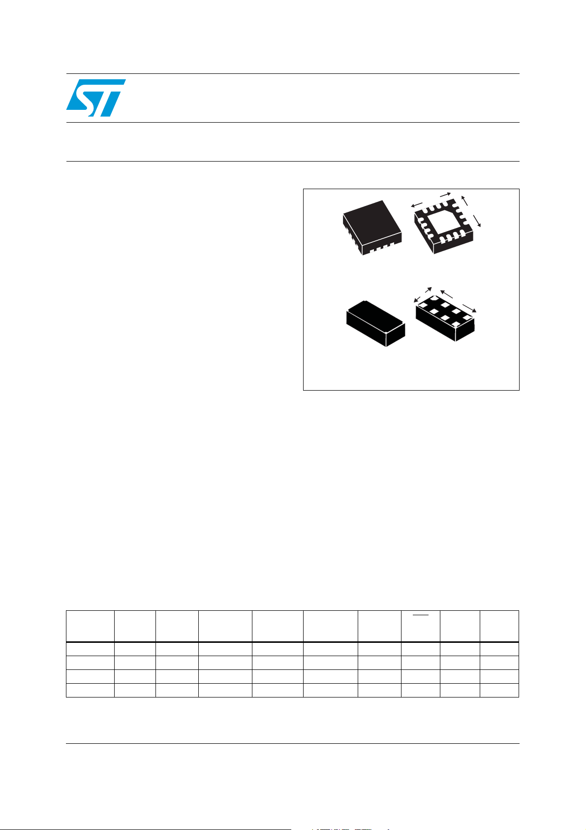
■ Two package options:
– Very small 3 mm x 3 mm, lead-free &
halogen-free (ECOPACK2
– Ultra-small 1.5 mm x 3.2 mm, lead-free &
halogen-free (ECOPACK2
leadless chip carrier with embedded
32 KHz crystal - no external oscillator
components required (M41T62)
QFN16
3 mm x 3 mm
1.5 mm
1.5 mm x 3.2 mm
n ±2 parts per million (±5
3.2 mm
®
) 16-lead QFN
®
) 8-pin ceramic
– 62.5 ms to 31 min timeout
Table 1. Device summary
Basic
RTC
M41T62 ✔✔ ✔ ✔ ✔ ✔✔
M41T63
1. Contact local ST sales office for availability.
(1)
✔✔ ✔ ✔ ✔ ✔ ✔
M41T64 ✔✔ ✔ ✔ ✔ ✔ ✔
M41T65 ✔✔ ✔ ✔ ✔ ✔✔
Alarms
OSC fail
detect
Watchdog
timer
Calibration
SQW
output
IRQ
output
WDO
output
F
32K
output
December 2011 Doc ID 10397 Rev 19 1/44
www.st.com
1

Contents M41T62/63/64/65
Contents
1 Description . . . . . . . . . . . . . . . . . . . . . . . . . . . . . . . . . . . . . . . . . . . . . . . . . 6
2 Operation . . . . . . . . . . . . . . . . . . . . . . . . . . . . . . . . . . . . . . . . . . . . . . . . . 12
2.1 2-wire bus characteristics . . . . . . . . . . . . . . . . . . . . . . . . . . . . . . . . . . . . . 12
2.1.1 Bus not busy . . . . . . . . . . . . . . . . . . . . . . . . . . . . . . . . . . . . . . . . . . . . . 12
2.1.2 Start data transfer . . . . . . . . . . . . . . . . . . . . . . . . . . . . . . . . . . . . . . . . . 12
2.1.3 Stop data transfer . . . . . . . . . . . . . . . . . . . . . . . . . . . . . . . . . . . . . . . . . 12
2.1.4 Data valid . . . . . . . . . . . . . . . . . . . . . . . . . . . . . . . . . . . . . . . . . . . . . . . . 13
2.1.5 Acknowledge . . . . . . . . . . . . . . . . . . . . . . . . . . . . . . . . . . . . . . . . . . . . . 13
2.2 READ mode . . . . . . . . . . . . . . . . . . . . . . . . . . . . . . . . . . . . . . . . . . . . . . . 14
2.3 WRITE mode . . . . . . . . . . . . . . . . . . . . . . . . . . . . . . . . . . . . . . . . . . . . . . 16
3 Clock operation . . . . . . . . . . . . . . . . . . . . . . . . . . . . . . . . . . . . . . . . . . . . 17
3.1 RTC registers . . . . . . . . . . . . . . . . . . . . . . . . . . . . . . . . . . . . . . . . . . . . . . 18
3.2 Calibrating the clock . . . . . . . . . . . . . . . . . . . . . . . . . . . . . . . . . . . . . . . . . 24
3.3 Setting alarm clock registers . . . . . . . . . . . . . . . . . . . . . . . . . . . . . . . . . . 26
3.4 Watchdog timer . . . . . . . . . . . . . . . . . . . . . . . . . . . . . . . . . . . . . . . . . . . . 27
3.5 Watchdog output (WDO - M41T63/65 only) . . . . . . . . . . . . . . . . . . . . . . . 27
3.6 Square wave output (M41T62/63/64) . . . . . . . . . . . . . . . . . . . . . . . . . . . . 28
3.7 Full-time 32 KHz square wave output (M41T64) . . . . . . . . . . . . . . . . . . . 28
3.8 Century bits . . . . . . . . . . . . . . . . . . . . . . . . . . . . . . . . . . . . . . . . . . . . . . . 29
3.9 Output driver pin (M41T62/65) . . . . . . . . . . . . . . . . . . . . . . . . . . . . . . . . . 29
3.10 Oscillator stop detection . . . . . . . . . . . . . . . . . . . . . . . . . . . . . . . . . . . . . . 29
3.11 Initial power-on defaults . . . . . . . . . . . . . . . . . . . . . . . . . . . . . . . . . . . . . . 30
4 Maximum ratings . . . . . . . . . . . . . . . . . . . . . . . . . . . . . . . . . . . . . . . . . . . 31
5 DC and AC parameters . . . . . . . . . . . . . . . . . . . . . . . . . . . . . . . . . . . . . . 32
6 Package mechanical information . . . . . . . . . . . . . . . . . . . . . . . . . . . . . . 36
7 Part numbering . . . . . . . . . . . . . . . . . . . . . . . . . . . . . . . . . . . . . . . . . . . . 42
2/44 Doc ID 10397 Rev 19

M41T62/63/64/65 Contents
8 Revision history . . . . . . . . . . . . . . . . . . . . . . . . . . . . . . . . . . . . . . . . . . . 43
Doc ID 10397 Rev 19 3/44

List of tables M41T62/63/64/65
List of tables
Table 1. Device summary . . . . . . . . . . . . . . . . . . . . . . . . . . . . . . . . . . . . . . . . . . . . . . . . . . . . . . . . . . 1
Table 2. Signal names . . . . . . . . . . . . . . . . . . . . . . . . . . . . . . . . . . . . . . . . . . . . . . . . . . . . . . . . . . . . 9
Table 3. M41T62 register map . . . . . . . . . . . . . . . . . . . . . . . . . . . . . . . . . . . . . . . . . . . . . . . . . . . . . 20
Table 4. M41T63 register map . . . . . . . . . . . . . . . . . . . . . . . . . . . . . . . . . . . . . . . . . . . . . . . . . . . . . 21
Table 5. M41T64 register map . . . . . . . . . . . . . . . . . . . . . . . . . . . . . . . . . . . . . . . . . . . . . . . . . . . . . 22
Table 6. M41T65 register map . . . . . . . . . . . . . . . . . . . . . . . . . . . . . . . . . . . . . . . . . . . . . . . . . . . . . 23
Table 7. Alarm repeat modes . . . . . . . . . . . . . . . . . . . . . . . . . . . . . . . . . . . . . . . . . . . . . . . . . . . . . . 26
Table 8. Square wave output frequency . . . . . . . . . . . . . . . . . . . . . . . . . . . . . . . . . . . . . . . . . . . . . . 28
Table 9. Initial power-on default values . . . . . . . . . . . . . . . . . . . . . . . . . . . . . . . . . . . . . . . . . . . . . . 30
Table 10. Century bits examples . . . . . . . . . . . . . . . . . . . . . . . . . . . . . . . . . . . . . . . . . . . . . . . . . . . . 30
Table 11. Absolute maximum ratings . . . . . . . . . . . . . . . . . . . . . . . . . . . . . . . . . . . . . . . . . . . . . . . . . 31
Table 12. Operating and AC measurement conditions. . . . . . . . . . . . . . . . . . . . . . . . . . . . . . . . . . . . 32
Table 13. Capacitance . . . . . . . . . . . . . . . . . . . . . . . . . . . . . . . . . . . . . . . . . . . . . . . . . . . . . . . . . . . . 33
Table 14. DC characteristics. . . . . . . . . . . . . . . . . . . . . . . . . . . . . . . . . . . . . . . . . . . . . . . . . . . . . . . . 33
Table 15. Crystal electrical characteristics . . . . . . . . . . . . . . . . . . . . . . . . . . . . . . . . . . . . . . . . . . . . . 34
Table 16. Crystals suitable for use with M41T6x series RTCs . . . . . . . . . . . . . . . . . . . . . . . . . . . . . . 34
Table 17. Oscillator characteristics. . . . . . . . . . . . . . . . . . . . . . . . . . . . . . . . . . . . . . . . . . . . . . . . . . . 35
Table 18. AC characteristics . . . . . . . . . . . . . . . . . . . . . . . . . . . . . . . . . . . . . . . . . . . . . . . . . . . . . . . . 35
Table 19. QFN16 – 16-pin, quad, flat package, no-lead, 3 mm x 3 mm body size, mechanical data. 37
Table 20. LCC8 — 8-pin, 1.5 mm x 3.2 mm leadless chip carrier, mechanical data . . . . . . . . . . . . . 39
Table 21. Carrier tape dimensions for QFN16 3 mm x 3 mm package. . . . . . . . . . . . . . . . . . . . . . . . 40
Table 22. Reel dimensions for 12 mm carrier tape - QFN16 and LCC8 packages. . . . . . . . . . . . . . . 41
Table 23. Ordering information scheme . . . . . . . . . . . . . . . . . . . . . . . . . . . . . . . . . . . . . . . . . . . . . . . 42
Table 24. Document revision history . . . . . . . . . . . . . . . . . . . . . . . . . . . . . . . . . . . . . . . . . . . . . . . . . 43
4/44 Doc ID 10397 Rev 19

M41T62/63/64/65 List of figures
List of figures
Figure 1. M41T62 logic diagram . . . . . . . . . . . . . . . . . . . . . . . . . . . . . . . . . . . . . . . . . . . . . . . . . . . . . 6
Figure 2. M41T63 logic diagram . . . . . . . . . . . . . . . . . . . . . . . . . . . . . . . . . . . . . . . . . . . . . . . . . . . . . 7
Figure 3. M41T64 logic diagram . . . . . . . . . . . . . . . . . . . . . . . . . . . . . . . . . . . . . . . . . . . . . . . . . . . . . 7
Figure 4. M41T65 logic diagram . . . . . . . . . . . . . . . . . . . . . . . . . . . . . . . . . . . . . . . . . . . . . . . . . . . . . 7
Figure 5. M41T62 connections . . . . . . . . . . . . . . . . . . . . . . . . . . . . . . . . . . . . . . . . . . . . . . . . . . . . . . 8
Figure 6. M41T63 connections . . . . . . . . . . . . . . . . . . . . . . . . . . . . . . . . . . . . . . . . . . . . . . . . . . . . . . 8
Figure 7. M41T64 connections . . . . . . . . . . . . . . . . . . . . . . . . . . . . . . . . . . . . . . . . . . . . . . . . . . . . . . 8
Figure 8. M41T65 connections . . . . . . . . . . . . . . . . . . . . . . . . . . . . . . . . . . . . . . . . . . . . . . . . . . . . . . 9
Figure 9. M41T62 block diagram . . . . . . . . . . . . . . . . . . . . . . . . . . . . . . . . . . . . . . . . . . . . . . . . . . . . . 9
Figure 10. M41T63 block diagram . . . . . . . . . . . . . . . . . . . . . . . . . . . . . . . . . . . . . . . . . . . . . . . . . . . . 10
Figure 11. M41T64 block diagram . . . . . . . . . . . . . . . . . . . . . . . . . . . . . . . . . . . . . . . . . . . . . . . . . . . . 10
Figure 12. M41T65 block diagram . . . . . . . . . . . . . . . . . . . . . . . . . . . . . . . . . . . . . . . . . . . . . . . . . . . . 10
Figure 13. Hardware hookup for SuperCap™ backup operation . . . . . . . . . . . . . . . . . . . . . . . . . . . . . 11
Figure 14. Serial bus data transfer sequence . . . . . . . . . . . . . . . . . . . . . . . . . . . . . . . . . . . . . . . . . . . 13
Figure 15. Acknowledgement sequence . . . . . . . . . . . . . . . . . . . . . . . . . . . . . . . . . . . . . . . . . . . . . . . 14
Figure 16. Slave address location . . . . . . . . . . . . . . . . . . . . . . . . . . . . . . . . . . . . . . . . . . . . . . . . . . . . 14
Figure 17. READ mode sequence . . . . . . . . . . . . . . . . . . . . . . . . . . . . . . . . . . . . . . . . . . . . . . . . . . . . 15
Figure 18. Alternative READ mode sequence . . . . . . . . . . . . . . . . . . . . . . . . . . . . . . . . . . . . . . . . . . . 15
Figure 19. WRITE mode sequence . . . . . . . . . . . . . . . . . . . . . . . . . . . . . . . . . . . . . . . . . . . . . . . . . . . 16
Figure 20. Buffer/transfer registers . . . . . . . . . . . . . . . . . . . . . . . . . . . . . . . . . . . . . . . . . . . . . . . . . . . 18
Figure 21. Crystal accuracy across temperature . . . . . . . . . . . . . . . . . . . . . . . . . . . . . . . . . . . . . . . . . 25
Figure 22. Calibration waveform . . . . . . . . . . . . . . . . . . . . . . . . . . . . . . . . . . . . . . . . . . . . . . . . . . . . . 25
Figure 23. Alarm interrupt reset waveform . . . . . . . . . . . . . . . . . . . . . . . . . . . . . . . . . . . . . . . . . . . . . . 26
Figure 24. AC measurement I/O waveform . . . . . . . . . . . . . . . . . . . . . . . . . . . . . . . . . . . . . . . . . . . . . 32
Figure 25. Crystal isolation example . . . . . . . . . . . . . . . . . . . . . . . . . . . . . . . . . . . . . . . . . . . . . . . . . . 32
Figure 26. Bus timing requirements sequence . . . . . . . . . . . . . . . . . . . . . . . . . . . . . . . . . . . . . . . . . . 35
Figure 27. QFN16 – 16-pin, quad, flat package, no-lead, 3 mm x 3 mm body size, outline . . . . . . . . 37
Figure 28. QFN16 – 16-pin, quad, flat package, no-lead, 3 x 3 mm, recommended footprint . . . . . . . 38
Figure 29. LCC8 — 8-pin, 1.5 mm x 3.2 mm leadless chip carrier, outline . . . . . . . . . . . . . . . . . . . . . 38
Figure 30. LCC8 — 8-pin, 1.5 mm x 3.2 mm leadless chip carrier, recommended footprint . . . . . . . . 39
Figure 31. Carrier tape for QFN16 3 mm x 3 mm package . . . . . . . . . . . . . . . . . . . . . . . . . . . . . . . . . 40
Figure 32. Carrier tape for LCC8 1.5 mm x 3.2 mm package . . . . . . . . . . . . . . . . . . . . . . . . . . . . . . . 40
Figure 33. Reel schematic . . . . . . . . . . . . . . . . . . . . . . . . . . . . . . . . . . . . . . . . . . . . . . . . . . . . . . . . . . 41
Doc ID 10397 Rev 19 5/44

Description M41T62/63/64/65
1 Description
The M41T6x is a low-power serial real-time clock (RTC) with a built-in 32.768 kHz oscillator.
Eight registers are used for the clock/calendar function and are configured in binary coded
decimal (BCD) format. An additional 8 registers provide status/control of alarm, 32 KHz
output, calibration, and watchdog functions. Addresses and data are transferred serially via
a two line, bidirectional I
automatically after each WRITE or READ data byte.
Functions available to the user include a time-of-day clock/calendar, alarm interrupts
(M41T62/65), 32 KHz output (M41T62/63/64), programmable square wave output
(M41T62/63/64), and watchdog output (M41T63/65). The eight clock address locations
contain the century, year, month, date, day, hour, minute, second and tenths/hundredths of a
second in 24 hour BCD format. Corrections for 28-, 29- (leap year), 30- and 31-day months
are made automatically.
The M41T6x is supplied in two very small packages: a tiny, 3 mm x 3 mm 16-pin QFN which
requires a user-supplied 32 KHz crystal, and an ultra-small 1.5 mm x 3.2 mm LCC with
embedded crystal - no external crystal is required.
Figure 1. M41T62 logic diagram
2
C interface. The built-in address register is incremented
V
CC
1. Open drain.
2. Defaults to 32 KHz on power-up.
3. Not bonded on LCC package.
XI
XO
SCL
SDA
(3)
(3)
M41T62
V
SS
IRQ/OUT
(2)
SQW
(1)
AI09103
6/44 Doc ID 10397 Rev 19

M41T62/63/64/65 Description
Figure 2. M41T63 logic diagram
V
CC
XI
XO
SCL
M41T63
WDO
SQW
(1)
(2)
SDA
V
SS
AI09189
1. Open drain.
2. Defaults to 32 KHz on power-up.
Figure 3. M41T64 logic diagram
V
CC
XI
XO
SCL
SDA
1. Open drain.
2. Defaults to 32 KHz on power-up.
Figure 4. M41T65 logic diagram
XI
XO
SCL
SDA
M41T64
V
SS
V
CC
M41T65
(1)
SQW
(2)
F
32K
(1)
WDO
IRQ/FT/OUT
AI09108
(1)
1. Open drain.
V
SS
AI09109
Doc ID 10397 Rev 19 7/44

Description M41T62/63/64/65
Figure 5. M41T62 connections
CC
15
NC
14
V
NC
13
12
NC
SDA
1
8
SCL
NC
16
XI
1
SQW
V
XO
SS
2
QFN
3
(1)
4
6
5
SS
V
7
NC
NC
11
IRQ/OUT
SCL
10
9
SDA
8
NC
1. SQW output defaults to 32 KHz upon power-up.
2. Open drain.
Figure 6. M41T63 connections
NC
16
XI
1
XO
2
V
3
SS
(1)
SQW
4
5
V
SS
15
14
7
SQW
CC
V
NC
13
V
NC
8
(1)
SS
NC
NC
12
11
10
2
LCC
3
4
7
6
5
NC
IRQ/OUT
V
CC
(2)
AI09100
NC
(2)
WDO
SCL
9
SDA
AI09190
(2)
NC
6
NC
1. SQW output defaults to 32 KHz upon power-up.
2. Open drain.
Figure 7. M41T64 connections
NC
NC
15
14
6
NC
16
XI
1
XO
2
V
3
SS
(1)
32K
4
F
5
SS
V
1. Enabled on power-up.
2. Open drain.
8/44 Doc ID 10397 Rev 19
CC
NC
V
13
NC
12
(2)
SQW
11
SCL
10
9
SDA
8
7
NC
NC
AI09101

M41T62/63/64/65 Description
Figure 8. M41T65 connections
15
CC
NC
V
14
6
7
NC
NC
WDO
NC
16
XI
1
XO
2
3
V
SS
(1)
4
5
SS
V
1. Open drain.
Table 2. Signal names
XI Oscillator input
XO Oscillator output
SDA Serial data input/output
SCL Serial clock input
IRQ/OUT Interrupt or OUT output (open drain)
/FT/OUT Interrupt, frequency test, or OUT output (open drain)
IRQ
SQW
F
32K
Programmable square wave - defaults to 32 KHz on power-up (open drain for
M41T64 only)
Dedicated 32 KHz output (M41T64 only)
WDO Watchdog timer output (open drain)
V
CC
V
SS
Supply voltage
Ground
13
NC
8
NC
NC
12
11
IRQ/FT/OUT
SCL
10
9
SDA
(1)
AI09102
Figure 9. M41T62 block diagram
(3)
XTAL
SDA
SCL
(3)
1. Open drain.
2. Defaults to 32 KHz on power-up.
3. Not bonded on embedded crystal (LCC) package.
32KHz
OSCILLATOR
I2C
INTERFACE
Doc ID 10397 Rev 19 9/44
REAL TIME CLOCK
CALENDAR
OSCILLATOR FAIL
DETECT
RTC W/ALARM
WATCHDOG
SQUARE WAVE
OFIE
AFE
SQWE
IRQ/OUT
(2)
SQW
AI08899a
(1)

Description M41T62/63/64/65
Figure 10. M41T63 block diagram
REAL TIME CLOCK
CALENDAR
OSCILLATOR FAIL
XTAL
32KHz
OSCILLATOR
DETECT
RTC W/ALARM
SDA
I2C
INTERFACE
SCL
1. Open drain.
2. Defaults to 32 KHz on power-up.
Figure 11. M41T64 block diagram
XTAL
SDA
SCL
1. Defaults enabled on power-up.
2. Open drain.
32KHz
OSCILLATOR
I2C
INTERFACE
WATCHDOG
SQUARE WAVE
REAL TIME CLOCK
CALENDAR
OSCILLATOR FAIL
DETECT
RTC W/ALARM
WATCHDOG
SQUARE WAVE
SQWE
32KE
SQWE
WDO
SQW
F
32K
SQW
(1)
(2)
AI09191
(1)
(2)
AI09192
Figure 12. M41T65 block diagram
XTAL
SDA
SCL
1. Open drain.
10/44 Doc ID 10397 Rev 19
32KHz
OSCILLATOR
I2C
INTERFACE
REAL TIME CLOCK
CALENDAR
OSCILLATOR FAIL
DETECT
RTC W/ALARM
WATCHDOG
OFIE
FT
AFE
IRQ/FT/OUT
(1)
WDO
AI09193
(1)

M41T62/63/64/65 Description
Figure 13. Hardware hookup for SuperCap™ backup operation
V
CC
(1)
MCU
V
CC
Por t
Reset Input
SQWIN
Serial Clock Line
Serial Data Line
32KHz CLKIN
AI10400b
V
XI
XO
V
CC
SS
M41T6x
IRQ/FT/OUT
WDO
SQW
F
(2)
(3)
(4)
SCL
SDA
32K
1. Diode required on open drain pin (M41T65 only) for SuperCap (or battery) backup. Low threshold BAT42
diode recommended.
2. For M41T62 and M41T65 (open drain).
3. For M41T63 and M41T65 (open drain).
4. For M41T64 (open drain).
Doc ID 10397 Rev 19 11/44

Operation M41T62/63/64/65
2 Operation
The M41T6x clock operates as a slave device on the serial bus. Access is obtained by
implementing a start condition followed by the correct slave address (D0h). The 16 bytes
contained in the device can then be accessed sequentially in the following order:
st
● 1
● 2
● 3
● 4
● 5
● 6
● 7
● 8
● 9
● 10
● 11
● 16th byte: flags register
byte: tenths/hundredths of a second register
nd
byte: seconds register
rd
byte: minutes register
th
byte: hours register
th
byte: square wave/day register
th
byte: date register
th
byte: century/month register
th
byte: year register
th
byte: calibration register
th
byte: watchdog register
th
- 15th bytes: alarm registers
2.1 2-wire bus characteristics
The bus is intended for communication between different ICs. It consists of two lines: a bidirectional data signal (SDA) and a clock signal (SCL). Both the SDA and SCL lines must be
connected to a positive supply voltage via a pull-up resistor.
The following protocol has been defined:
● Data transfer may be initiated only when the bus is not busy.
● During data transfer, the data line must remain stable whenever the clock line is high.
● Changes in the data line, while the clock line is high, will be interpreted as control
signals.
Accordingly, the following bus conditions have been defined:
2.1.1 Bus not busy
Both data and clock lines remain high.
2.1.2 Start data transfer
A change in the state of the data line, from high to low, while the clock is high, defines the
START condition.
2.1.3 Stop data transfer
A change in the state of the data line, from low to high, while the clock is high, defines the
STOP condition.
12/44 Doc ID 10397 Rev 19

M41T62/63/64/65 Operation
2.1.4 Data valid
The state of the data line represents valid data when after a start condition, the data line is
stable for the duration of the high period of the clock signal. The data on the line may be
changed during the Low period of the clock signal. There is one clock pulse per bit of data.
Each data transfer is initiated with a start condition and terminated with a stop condition.
The number of data bytes transferred between the start and stop conditions is not limited.
The information is transmitted byte-wide and each receiver acknowledges with a ninth bit.
By definition a device that gives out a message is called “transmitter,” the receiving device
that gets the message is called “receiver.” The device that controls the message is called
“master.” The devices that are controlled by the master are called “slaves.”
2.1.5 Acknowledge
Each byte of eight bits is followed by one acknowledge bit. This acknowledge bit is a low
level put on the bus by the receiver whereas the master generates an extra acknowledge
related clock pulse. A slave receiver which is addressed is obliged to generate an
acknowledge after the reception of each byte that has been clocked out of the slave
transmitter.
The device that acknowledges has to pull down the SDA line during the acknowledge clock
pulse in such a way that the SDA line is a stable Low during the high period of the
acknowledge related clock pulse. Of course, setup and hold times must be taken into
account. A master receiver must signal an end of data to the slave transmitter by not
generating an acknowledge on the last byte that has been clocked out of the slave. In this
case the transmitter must leave the data line high to enable the master to generate the
STOP condition.
Figure 14. Serial bus data transfer sequence
DATA LINE
STABLE
DATA VALID
CLOCK
DATA
STA RT
CONDITION
CHANGE OF
DATA ALLOWED
STOP
CONDITION
AI00587
Doc ID 10397 Rev 19 13/44

Operation M41T62/63/64/65
Figure 15. Acknowledgement sequence
CLOCK PULSE FOR
ACKNOWLEDGEMENT
SCL FROM
MASTER
START
12 89
DATA OUTPUT
BY TRANSMITTER
DATA OUTPUT
BY RECEIVER
2.2 READ mode
In this mode the master reads the M41T6x slave after setting the slave address (see
Figure 17 on page 15). Following the WRITE mode control bit (R/W
acknowledge bit, the word address 'An' is written to the on-chip address pointer. Next the
START condition and slave address are repeated followed by the READ mode control bit
(R/W
=1). At this point the master transmitter becomes the master receiver. The data byte
which was addressed will be transmitted and the master receiver will send an acknowledge
bit to the slave transmitter. the address pointer is only incremented on reception of an
acknowledge clock. The M41T6x slave transmitter will now place the data byte at address
An+1 on the bus, the master receiver reads and acknowledges the new byte and the
address pointer is incremented to “An+2.”
This cycle of reading consecutive addresses will continue until the master receiver sends a
STOP condition to the slave transmitter.
The system-to-user transfer of clock data will be halted whenever the address being read is
a clock address (00h to 07h). The update will resume due to a stop condition or when the
pointer increments to any non-clock address (08h-0Fh).
MSB LSB
AI00601
=0) and the
Note: This is true both in READ mode and WRITE mode.
An alternate READ mode may also be implemented whereby the master reads the M41T6x
slave without first writing to the (volatile) address pointer. The first address that is read is the
last one stored in the pointer (see Figure 18 on page 15).
Figure 16. Slave address location
STA RT A
14/44 Doc ID 10397 Rev 19
SLAVE ADDRESS
MSB
0100 011
R/W
LSB
AI00602
 Loading...