

M41ST87Y
M41ST87W
5.0 V and 3.3/3.0 V secure serial RTC and NVRAM supervisor
with tamper detection and 128 bytes of clearable NVRAM
Features
■ 5.0, 3.3, or 3.0 V operation
■ 400 kHz I
■ NVRAM supervisor to non-volatize external
LPSRAM
■ 2.5 to 5.5 V oscillator operating voltage
■ Automatic switchover and deselect circuitry
■ Choice of power-fail deselect voltages
– M41ST87Y:
– M41ST87W:
■ Two independent power-fail comparators
(1.25 V reference)
■ Counters for tenths/hundredths of seconds,
seconds, minutes, hours, day, date, month,
year, and century
■ 128 bytes of clearable, general purpose
NVRAM
■ Programmable alarm and interrupt function
(valid even during battery backup mode)
■ Programmable watchdog timer
■ Unique electronic serial number (8-byte)
■ 32 kHz frequency output available upon power-
on
■ Microprocessor power-on reset output
■ Battery low flag
■ Ultra-low battery supply current of 500 nA (typ)
2
C bus
(not recommended for new design, contact
ST sales office for availability)
THS = 1: V
THS = 0: V
THS = 1: V
THS = 0: V
≈ 4.63 V; VCC = 4.75 to 5.5 V
PFD
≈ 4.37 V; VCC = 4.5 to 5.5 V
PFD
≈ 2.9 V; VCC = 3.0 to 3.6 V
PFD
≈ 2.63 V; VCC = 2.7 to 3.6 V
PFD
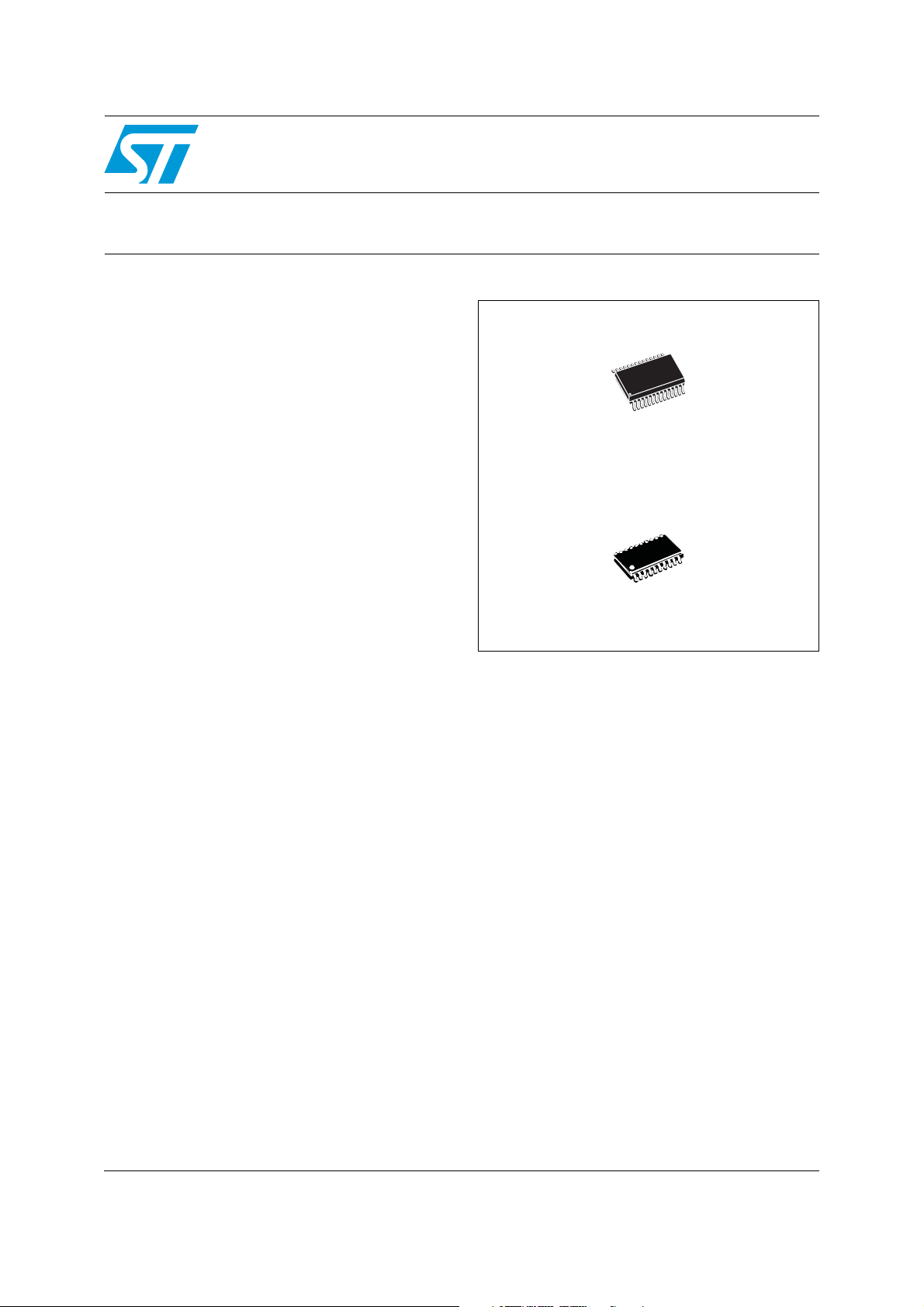
Embedded crystal
28-pin, (300 mil)
SOX28
SSOP20
Security features
■ Tamper indication circuits with timestamp and
RAM clear
■ LPSRAM clear function (TP
■ Packaging includes a 28-lead, embedded
crystal SOIC and a 20-lead SSOP
■ Oscillator stop detection
CLR
)
October 2011 Doc ID 9497 Rev 10 1/54
www.st.com
1

Contents M41ST87Y, M41ST87W
Contents
1 Description . . . . . . . . . . . . . . . . . . . . . . . . . . . . . . . . . . . . . . . . . . . . . . . . . 6
1.1 Security features . . . . . . . . . . . . . . . . . . . . . . . . . . . . . . . . . . . . . . . . . . . . 6
2 Operating modes . . . . . . . . . . . . . . . . . . . . . . . . . . . . . . . . . . . . . . . . . . . 12
2.1 2-wire bus characteristics . . . . . . . . . . . . . . . . . . . . . . . . . . . . . . . . . . . . . 13
2.1.1 Bus not busy . . . . . . . . . . . . . . . . . . . . . . . . . . . . . . . . . . . . . . . . . . . . . 13
2.1.2 Start data transfer . . . . . . . . . . . . . . . . . . . . . . . . . . . . . . . . . . . . . . . . . 13
2.1.3 Stop data transfer . . . . . . . . . . . . . . . . . . . . . . . . . . . . . . . . . . . . . . . . . 13
2.1.4 Data valid . . . . . . . . . . . . . . . . . . . . . . . . . . . . . . . . . . . . . . . . . . . . . . . . 13
2.1.5 Acknowledge . . . . . . . . . . . . . . . . . . . . . . . . . . . . . . . . . . . . . . . . . . . . . 13
2.2 READ mode . . . . . . . . . . . . . . . . . . . . . . . . . . . . . . . . . . . . . . . . . . . . . . . 15
2.3 WRITE mode . . . . . . . . . . . . . . . . . . . . . . . . . . . . . . . . . . . . . . . . . . . . . . 17
2.4 Data retention mode . . . . . . . . . . . . . . . . . . . . . . . . . . . . . . . . . . . . . . . . . 17
2.5 Tamper detection circuit . . . . . . . . . . . . . . . . . . . . . . . . . . . . . . . . . . . . . . 18
2.6 Tamper register bits (tamper 1 and tamper 2) . . . . . . . . . . . . . . . . . . . . . 18
2.6.1 Tamper enable bits (TEB1 and TEB2) . . . . . . . . . . . . . . . . . . . . . . . . . . 18
2.6.2 Tamper bits (TB1 and TB2) . . . . . . . . . . . . . . . . . . . . . . . . . . . . . . . . . . 19
2.6.3 Tamper interrupt enable bits (TIE1 and TIE2) . . . . . . . . . . . . . . . . . . . . 19
2.6.4 Tamper connect mode bit (TCM1 and TCM2) . . . . . . . . . . . . . . . . . . . . 19
2.6.5 Tamper polarity mode bits (TPM1 and TPM2) . . . . . . . . . . . . . . . . . . . . 19
2.6.6 Tamper detect sampling (TDS1 and TDS2) . . . . . . . . . . . . . . . . . . . . . . 22
2.6.7 Tamper current high/tamper current low (TCHI/TCLO1 and
TCHI/TCLO2) . . . . . . . . . . . . . . . . . . . . . . . . . . . . . . . . . . . . . . . . . . . . . 22
2.6.8 RAM clear (CLR1 and CLR2) . . . . . . . . . . . . . . . . . . . . . . . . . . . . . . . . 22
2.6.9 RAM clear external (CLR1
package only . . . . . . . . . . . . . . . . . . . . . . . . . . . . . . . . . . . . . . . . . . . . . 22
and CLR2
EXT
) - available in SOX28
EXT
2.7 Tamper detection operation . . . . . . . . . . . . . . . . . . . . . . . . . . . . . . . . . . . 26
2.8 Sampling . . . . . . . . . . . . . . . . . . . . . . . . . . . . . . . . . . . . . . . . . . . . . . . . . 26
2.9 Internal tamper pull-up/down current . . . . . . . . . . . . . . . . . . . . . . . . . . . . 27
2.10 Avoiding inadvertent tampers (normally closed configuration) . . . . . . . . . 27
2.11 Tamper event time-stamp . . . . . . . . . . . . . . . . . . . . . . . . . . . . . . . . . . . . . 28
3 Clock operation . . . . . . . . . . . . . . . . . . . . . . . . . . . . . . . . . . . . . . . . . . . . 29
3.0.1 Power-down time-stamp . . . . . . . . . . . . . . . . . . . . . . . . . . . . . . . . . . . . 29
2/54 Doc ID 9497 Rev 10

M41ST87Y, M41ST87W Contents
3.1 TIMEKEEPER® registers . . . . . . . . . . . . . . . . . . . . . . . . . . . . . . . . . . . . . 30
3.2 Calibrating the clock . . . . . . . . . . . . . . . . . . . . . . . . . . . . . . . . . . . . . . . . . 31
3.3 Setting alarm clock registers . . . . . . . . . . . . . . . . . . . . . . . . . . . . . . . . . . 33
3.4 Watchdog timer . . . . . . . . . . . . . . . . . . . . . . . . . . . . . . . . . . . . . . . . . . . . 35
3.5 Square wave output . . . . . . . . . . . . . . . . . . . . . . . . . . . . . . . . . . . . . . . . . 36
3.6 Full-time 32 kHz square wave output . . . . . . . . . . . . . . . . . . . . . . . . . . . . 37
3.7 Power-on reset . . . . . . . . . . . . . . . . . . . . . . . . . . . . . . . . . . . . . . . . . . . . . 37
3.8 Reset inputs (RSTIN1
3.9 Power-fail comparators (1 and 2) . . . . . . . . . . . . . . . . . . . . . . . . . . . . . . . 38
3.10 Power-fail outputs . . . . . . . . . . . . . . . . . . . . . . . . . . . . . . . . . . . . . . . . . . . 38
3.11 Century bits . . . . . . . . . . . . . . . . . . . . . . . . . . . . . . . . . . . . . . . . . . . . . . . 39
3.12 Output driver pin . . . . . . . . . . . . . . . . . . . . . . . . . . . . . . . . . . . . . . . . . . . . 39
3.13 Battery low warning . . . . . . . . . . . . . . . . . . . . . . . . . . . . . . . . . . . . . . . . . 39
3.14 t
3.15 Electronic serial number . . . . . . . . . . . . . . . . . . . . . . . . . . . . . . . . . . . . . . 40
3.16 Oscillator stop detection . . . . . . . . . . . . . . . . . . . . . . . . . . . . . . . . . . . . . . 40
3.17 Initial power-on defaults . . . . . . . . . . . . . . . . . . . . . . . . . . . . . . . . . . . . . . 41
bit . . . . . . . . . . . . . . . . . . . . . . . . . . . . . . . . . . . . . . . . . . . . . . . . . . . . 40
rec
& RSTIN2) . . . . . . . . . . . . . . . . . . . . . . . . . . . . . . 37
4 Maximum ratings . . . . . . . . . . . . . . . . . . . . . . . . . . . . . . . . . . . . . . . . . . . 42
5 DC and AC parameters . . . . . . . . . . . . . . . . . . . . . . . . . . . . . . . . . . . . . . 43
6 Package mechanical data . . . . . . . . . . . . . . . . . . . . . . . . . . . . . . . . . . . . 47
7 Part numbering . . . . . . . . . . . . . . . . . . . . . . . . . . . . . . . . . . . . . . . . . . . . 51
8 References . . . . . . . . . . . . . . . . . . . . . . . . . . . . . . . . . . . . . . . . . . . . . . . . 52
9 Revision history . . . . . . . . . . . . . . . . . . . . . . . . . . . . . . . . . . . . . . . . . . . 53
Doc ID 9497 Rev 10 3/54

List of tables M41ST87Y, M41ST87W
List of tables
Table 1. Signal names . . . . . . . . . . . . . . . . . . . . . . . . . . . . . . . . . . . . . . . . . . . . . . . . . . . . . . . . . . . . 9
Table 2. AC characteristics . . . . . . . . . . . . . . . . . . . . . . . . . . . . . . . . . . . . . . . . . . . . . . . . . . . . . . . . 15
Table 3. Tamper detection truth table . . . . . . . . . . . . . . . . . . . . . . . . . . . . . . . . . . . . . . . . . . . . . . . . 20
Table 4. Tamper detection current (normally closed - TCM
Table 5. Tamper detect timing . . . . . . . . . . . . . . . . . . . . . . . . . . . . . . . . . . . . . . . . . . . . . . . . . . . . . 25
Table 6. Calculated cut-off frequency for typical capacitance and resistance values. . . . . . . . . . . . 27
Table 7. TIMEKEEPER
Table 8. Alarm repeat modes . . . . . . . . . . . . . . . . . . . . . . . . . . . . . . . . . . . . . . . . . . . . . . . . . . . . . . 34
Table 9. Square wave output frequency . . . . . . . . . . . . . . . . . . . . . . . . . . . . . . . . . . . . . . . . . . . . . . 36
Table 10. Reset AC characteristics . . . . . . . . . . . . . . . . . . . . . . . . . . . . . . . . . . . . . . . . . . . . . . . . . . 38
Table 11. Century bits examples . . . . . . . . . . . . . . . . . . . . . . . . . . . . . . . . . . . . . . . . . . . . . . . . . . . . 39
Table 12. t
Table 13. Default values . . . . . . . . . . . . . . . . . . . . . . . . . . . . . . . . . . . . . . . . . . . . . . . . . . . . . . . . . . . 41
Table 14. Absolute maximum ratings . . . . . . . . . . . . . . . . . . . . . . . . . . . . . . . . . . . . . . . . . . . . . . . . . 42
Table 15. DC and AC measurement conditions . . . . . . . . . . . . . . . . . . . . . . . . . . . . . . . . . . . . . . . . . 43
Table 16. Capacitance . . . . . . . . . . . . . . . . . . . . . . . . . . . . . . . . . . . . . . . . . . . . . . . . . . . . . . . . . . . . 43
Table 17. DC characteristics. . . . . . . . . . . . . . . . . . . . . . . . . . . . . . . . . . . . . . . . . . . . . . . . . . . . . . . . 44
Table 18. Crystal electrical characteristics . . . . . . . . . . . . . . . . . . . . . . . . . . . . . . . . . . . . . . . . . . . . . 45
Table 19. Power down/up AC characteristics . . . . . . . . . . . . . . . . . . . . . . . . . . . . . . . . . . . . . . . . . . . 46
Table 20. SOX28 – 28-lead plastic small outline, 300 mils, embedded crystal mechanical data . . . . 47
Table 21. SSOP20 – 20-lead, shrink, small outline package mechanical data. . . . . . . . . . . . . . . . . . 48
Table 22. Carrier tape dimensions for SOX28 package . . . . . . . . . . . . . . . . . . . . . . . . . . . . . . . . . . . 49
Table 23. Reel dimensions for 24 mm carrier tape (SOX28 package) and 16 mm carrier tape
Table 24. Ordering information scheme . . . . . . . . . . . . . . . . . . . . . . . . . . . . . . . . . . . . . . . . . . . . . . . 51
Table 25. Document revision history . . . . . . . . . . . . . . . . . . . . . . . . . . . . . . . . . . . . . . . . . . . . . . . . . 53
definitions . . . . . . . . . . . . . . . . . . . . . . . . . . . . . . . . . . . . . . . . . . . . . . . . . . . . . . . . . . . 40
rec
(SSOP20 package) . . . . . . . . . . . . . . . . . . . . . . . . . . . . . . . . . . . . . . . . . . . . . . . . . . . . . . . 50
®
register map . . . . . . . . . . . . . . . . . . . . . . . . . . . . . . . . . . . . . . . . . . . . . . . 30
= '0') . . . . . . . . . . . . . . . . . . . . . . . . . . 23
X
4/54 Doc ID 9497 Rev 10

M41ST87Y, M41ST87W List of figures
List of figures
Figure 1. Logic diagram . . . . . . . . . . . . . . . . . . . . . . . . . . . . . . . . . . . . . . . . . . . . . . . . . . . . . . . . . . . . 7
Figure 2. 28-pin, 300 mil SOIC connections . . . . . . . . . . . . . . . . . . . . . . . . . . . . . . . . . . . . . . . . . . . . 8
Figure 3. 20-pin, SSOP connections . . . . . . . . . . . . . . . . . . . . . . . . . . . . . . . . . . . . . . . . . . . . . . . . . . 8
Figure 4. Block diagram . . . . . . . . . . . . . . . . . . . . . . . . . . . . . . . . . . . . . . . . . . . . . . . . . . . . . . . . . . . 10
Figure 5. Hardware hookup . . . . . . . . . . . . . . . . . . . . . . . . . . . . . . . . . . . . . . . . . . . . . . . . . . . . . . . . 11
Figure 6. Serial bus data transfer sequence . . . . . . . . . . . . . . . . . . . . . . . . . . . . . . . . . . . . . . . . . . . 14
Figure 7. Acknowledgement sequence . . . . . . . . . . . . . . . . . . . . . . . . . . . . . . . . . . . . . . . . . . . . . . . 14
Figure 8. Bus timing requirements sequence . . . . . . . . . . . . . . . . . . . . . . . . . . . . . . . . . . . . . . . . . . 14
Figure 9. Slave address location . . . . . . . . . . . . . . . . . . . . . . . . . . . . . . . . . . . . . . . . . . . . . . . . . . . . 16
Figure 10. READ mode sequence . . . . . . . . . . . . . . . . . . . . . . . . . . . . . . . . . . . . . . . . . . . . . . . . . . . . 16
Figure 11. Alternate READ mode sequence . . . . . . . . . . . . . . . . . . . . . . . . . . . . . . . . . . . . . . . . . . . . 16
Figure 12. WRITE mode sequence . . . . . . . . . . . . . . . . . . . . . . . . . . . . . . . . . . . . . . . . . . . . . . . . . . . 17
Figure 13. WRITE cycle timing: RTC & external SRAM control signals. . . . . . . . . . . . . . . . . . . . . . . . 17
Figure 14. Tamper detect connection options . . . . . . . . . . . . . . . . . . . . . . . . . . . . . . . . . . . . . . . . . . . 20
Figure 15. Basic tamper detect options . . . . . . . . . . . . . . . . . . . . . . . . . . . . . . . . . . . . . . . . . . . . . . . . 21
Figure 16. Tamper detect output options . . . . . . . . . . . . . . . . . . . . . . . . . . . . . . . . . . . . . . . . . . . . . . . 21
Figure 17. Tamper detect sampling options. . . . . . . . . . . . . . . . . . . . . . . . . . . . . . . . . . . . . . . . . . . . . 23
Figure 18. Tamper current options. . . . . . . . . . . . . . . . . . . . . . . . . . . . . . . . . . . . . . . . . . . . . . . . . . . . 24
Figure 19. Tamper output timing (with CLR1
package only. . . . . . . . . . . . . . . . . . . . . . . . . . . . . . . . . . . . . . . . . . . . . . . . . . . . . . . . . . . . 24
Figure 20. RAM clear hardware hookup (SOX28 package only) . . . . . . . . . . . . . . . . . . . . . . . . . . . . . 25
Figure 21. Low-pass filter implementation for noise immunity . . . . . . . . . . . . . . . . . . . . . . . . . . . . . . . 27
Figure 22. Crystal accuracy across temperature . . . . . . . . . . . . . . . . . . . . . . . . . . . . . . . . . . . . . . . . . 33
Figure 23. Calibration waveform . . . . . . . . . . . . . . . . . . . . . . . . . . . . . . . . . . . . . . . . . . . . . . . . . . . . . 33
Figure 24. Alarm interrupt reset waveform . . . . . . . . . . . . . . . . . . . . . . . . . . . . . . . . . . . . . . . . . . . . . . 34
Figure 25. Backup mode alarm waveform . . . . . . . . . . . . . . . . . . . . . . . . . . . . . . . . . . . . . . . . . . . . . . 35
Figure 26. RSTIN1
Figure 27. AC testing input/output waveforms . . . . . . . . . . . . . . . . . . . . . . . . . . . . . . . . . . . . . . . . . . . 43
Figure 28. Power down/up mode AC waveforms. . . . . . . . . . . . . . . . . . . . . . . . . . . . . . . . . . . . . . . . . 46
Figure 29. SOX28 – 28-lead plastic small outline, 300 mils, embedded crystal outline. . . . . . . . . . . . 47
Figure 30. SSOP20 – 20-lead, shrink, small outline package outline . . . . . . . . . . . . . . . . . . . . . . . . . 48
Figure 31. Carrier tape for SOX28 package . . . . . . . . . . . . . . . . . . . . . . . . . . . . . . . . . . . . . . . . . . . . 49
Figure 32. Carrier tape for SSOP20 package . . . . . . . . . . . . . . . . . . . . . . . . . . . . . . . . . . . . . . . . . . . 49
Figure 33. Reel schematic . . . . . . . . . . . . . . . . . . . . . . . . . . . . . . . . . . . . . . . . . . . . . . . . . . . . . . . . . . 50
& RSTIN2 timing waveforms . . . . . . . . . . . . . . . . . . . . . . . . . . . . . . . . . . . . . . . . . 37
or CLR2
EXT
= '1') - available in SOX28
EXT
Doc ID 9497 Rev 10 5/54

Description M41ST87Y, M41ST87W
1 Description
The M41ST87Y/W secure serial RTC and NVRAM supervisor is a low power 1280-bit, static
CMOS SRAM organized as 160 bytes by 8 bits. A built-in 32.768 kHz oscillator (internal
crystal-controlled) and 8 bytes of the SRAM are used for the clock/calendar function and are
configured in binary coded decimal (BCD) format.
An additional 11 bytes of RAM provide calibration, status/control of alarm, watchdog,
tamper, and square wave functions. 8 bytes of ROM and finally 128 bytes of user RAM are
also provided. Addresses and data are transferred serially via a two line, bidirectional I
interface. The built-in address register is incremented automatically after each WRITE or
READ data byte. The M41ST87Y/W has a built-in power sense circuit which detects power
failures and automatically switches to the battery supply when a power failure occurs. The
energy needed to sustain the SRAM and clock operations can be supplied by a small lithium
button-cell supply when a power failure occurs.
Functions available to the user include a non-volatile, time-of-day clock/calendar, alarm
interrupts, tamper detection, watchdog timer, and programmable square wave output. Other
features include a power-on reset as well as two additional debounced inputs (RSTIN1
RSTIN2
contain the century, year, month, date, day, hour, minute, second and tenths/hundredths of a
second in 24-hour BCD format. Corrections for 28, 29 (leap year), 30 and 31 day months are
made automatically.
) which can also generate an output reset (RST). The eight clock address locations
2
C
and
1.1 Security features
Two fully independent tamper detection Inputs allow monitoring of multiple locations within
the system. User programmable bits provide both normally open and normally closed switch
monitoring. Time stamping of the tamper event is automatically provided. There is also an
option allowing data stored in either internal memory (128 bytes), and/or external memory to
be cleared, protecting sensitive information in the event tampering occurs. By embedding
the 32 kHz crystal in the SOX28 package, the clock is completely isolated from external
tampering. An oscillator fail bit (OF) is also provided to ensure correct operation of the
oscillator.
The M41ST87Y/W is supplied in a 28-pin, 300 mil SOIC package which includes an
embedded 32 kHz crystal and a 20-pin SSOP package for use with an external crystal.
The SOIC and SSOP packages are shipped in plastic anti-static tubes or in tape & reel form.
The 300 mil, embedded crystal SOIC requires only a user-supplied battery to provide non-
volatile operation.
6/54 Doc ID 9497 Rev 10
M41ST87Y, M41ST87W Description
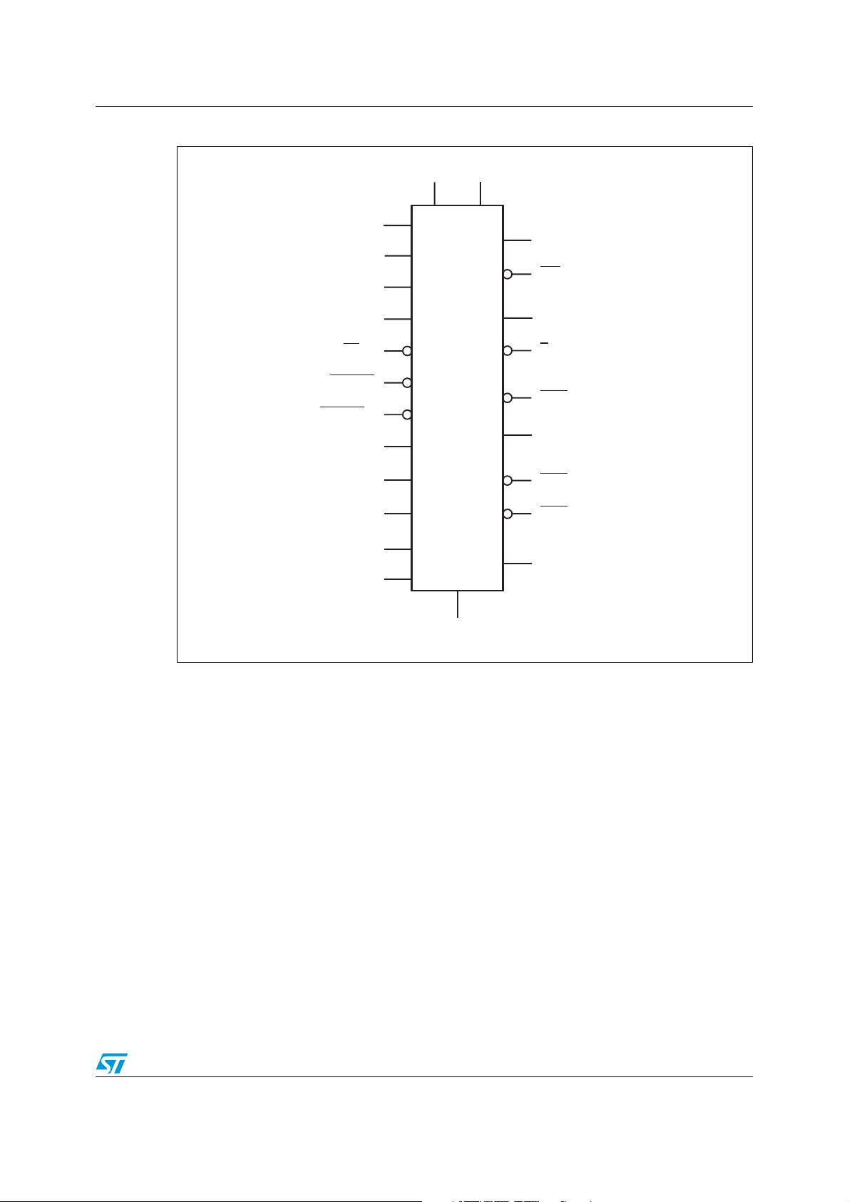
Figure 1. Logic diagram
XI
XO
SCL
SDA
EX
RSTIN1
RSTIN2
WDI
PFI
PFI
TP1
TP2
(4)
(4)
(3)
IN
IN
(3)
(3)
1
2
CC
V
BAT
V
M41ST87Y
M41ST87W
V
OUT
IRQ/OUT
SQW/FT
(3)
E
CON
(1)
RST
(1)
F
32k
(2)
PFO
1
(2)
PFO
2
(3)
TP
CLR
(1)
(2)
V
SS
1. Open drain output.
2. Programmable output (open drain or full-CMOS). Defaults to open drain on first power-up.
3. Available in SOX28 package only.
4. Available in SSOP package only.
AI07023
Doc ID 9497 Rev 10 7/54
Description M41ST87Y, M41ST87W
Figure 2. 28-pin, 300 mil SOIC connections
V
NF
NF
NF
NF
NC
NC
PFO
SQW/FT
WDI
RSTIN1
RSTIN2
PFO
PFI
V
SS
1
2
3
4
5
6
7
2
M41ST87Y
8
M41ST87W
9
10
11
12
1
13
2
14
28
27
26
25
24
23
22
21
20
19
18
17
16
15
CC
EX
IRQ/OUT
V
OUT
TP2
IN
PFI
1
SCL
F
32k
TP1
IN
RST
TP
CLR
SDA
E
CON
V
BAT
AI07025b
Note: No function (NF) and no connect (NC) pins should be tied to V
internally shorted together.
Figure 3. 20-pin, SSOP connections
V
CC
X1
X2
NC
PFO
SQW/FT
RSTIN1
PFO
PFI
V
SS
Note: No connect (NC) pin should be tied to V
1
2
3
4
5
2
M41ST87Y
M41ST87W
6
7
8
1
9
2
10
.
SS
20
19
18
17
16
15
14
13
12
11
IRQ/OUT
V
OUT
TP2
PFI
SCL
F
32k
TP1
RST
SDA
V
BAT
AI07025c
. Pins 1, 2, 3, and 4 are
SS
IN
1
IN
8/54 Doc ID 9497 Rev 10

M41ST87Y, M41ST87W Description
Table 1. Signal names
(1)
XI
(1)
XO
(2)
E
CON
(2)
EX
IRQ/OUT
(3)
Oscillator input
Oscillator output
Conditioned chip enable output
External chip enable
Interrupt/out output (open drain)
PFI
PFI
PFO
PFO
RST
1
2
(4)
1
(4)
2
(3)
Power fail input 1
Power fail input 2
Power fail output 1
Power fail output 2
Reset output (open drain)
RSTIN1 Reset 1 input
RSTIN2
(2)
Reset 2 input
SCL Serial clock input
SDA Serial data input/output
CC
OUT
SS
32k
CLR
BAT
(5)
(5)
(4)
(2)
Square wave output/frequency test
Watchdog input
Supply voltage
Voltage output
Ground
(3)
IN
IN
(2)
32 kHz square wave output (open drain)
Tamper pin 1 input
Tamper pin 2 input
Tamper pin RAM clear
Positive battery pin input
No function
No connect
SQW/FT
WDI
V
V
V
F
TP1
TP2
TP
V
NF
NC
1. Available in SSOP package only.
2. Available in SOX28 package only.
3. Open drain output.
4. Programmable output (open drain or full-CMOS).
5. Should be connected to VSS.
Doc ID 9497 Rev 10 9/54
Description M41ST87Y, M41ST87W
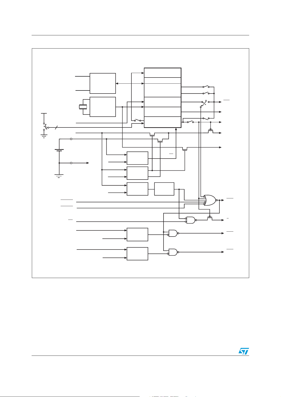
Figure 4. Block diagram
REAL TIME CLOCK
CALENDAR
128 BYTES
SDA
I2C
INTERFACE
SCL
(4)
Crystal
V
OUT
WDI
2
TPX
V
IN
CC
V
BAT
V
SS
XI
32KHz
OSCILLATOR
XO
(3)
V
BL
CLR
COMPARE
USER RAM
8 BYTES ROM
RTC w/ALARM
& CALIBRATION
WATCHDOG
SQUARE WAVE
X
TAMPER
BL
OFIE
AFE
WDS
CLRX
EXT
TIE
OUT
32k
CLR
(1)
(2)
(3)
(1)
IRQ/OUT
X
SQW/FT
TP
V
F
SO
PFD
COMPARE
COMPARE
COMPARE
POR
RST
E
CON
PFO
RSTIN1
RSTIN2
EX
PFI
V
V
(3)
(3)
1
1.25V
(Internal)
PFI
2
COMPARE
PFO
1.25V
(Internal)
AI07026
1. Open drain output.
2. Programmable output (open drain or full-CMOS); if open drain option is selected and if pulled-up to supply other than V
this supply must be equal to, or less than V
when VCC = 0 V (during battery backup mode).
BAT
3. Available in SOX28 package only.
4. Crystal is external on SSOP package and internal for the SOX28 package.
(1)
(3)
(2)
1
(2)
2
,
CC
10/54 Doc ID 9497 Rev 10
M41ST87Y, M41ST87W Description
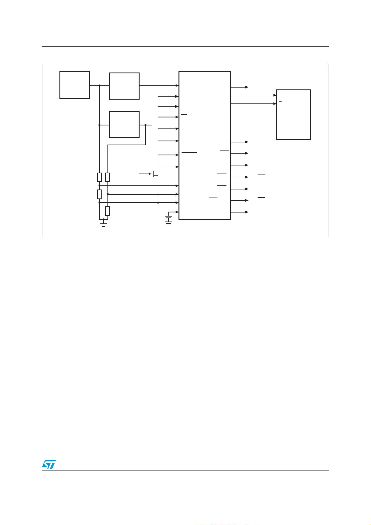
Figure 5. Hardware hookup
Unregulated
Voltage
V
IN
Regulator
V
IN
3.3V
Regulator
For monitoring
of additional
voltage sources
Pushbutton
R1
R3
R2
R4
1. Available in SOX28 package only.
5V
Reset
M41ST87Y/W
V
CC
V
CC
V
CC
TP1
TP2
EX
SCL
WDI
IN
IN
(1)
(1)
RSTIN1
(1)
RSTIN2
PFI
1
PFI
2
V
SS
V
BAT
TP
CLR
V
OUT
E
CON
SDA
RST
SQW/FT
PFO
PFO
IRQ/OUT
F
32k
(1)
V
(1)
CC
E
Low-Power
SRAM
To Microprocessor
To LED Display
1
2
To NMI
To INT
To 32kHz
AI07027
Doc ID 9497 Rev 10 11/54

Operating modes M41ST87Y, M41ST87W
2 Operating modes
The M41ST87Y/W clock operates as a slave device on the serial bus. Access is obtained by
implementing a start condition followed by the correct slave address (D0h). The 160 bytes
contained in the device can then be accessed sequentially in the following order:
00h. Tenths/hundredths of a second register
01h. Seconds register
02h. Minutes register
03h. Century/hours register
04h. Day register
05h. Date register
06h. Month register
07h. Year register
08h. Control register
09h. Watchdog register
0Ah-0Eh. Alarm registers
0Fh. Flag register
10h-12h. Reserved
13h. Square wave
14h. Tamper register 1
15h. Tamper register 2
16h-1Dh. Serial number (8 bytes)
1Eh-1Fh. Reserved (2 bytes)
20h-9Fh. User RAM (128 bytes)
The M41ST87Y/W clock continually monitors V
V
fall below V
CC
, the device terminates an access in progress and resets the device
PFD
for an out-of-tolerance condition. Should
CC
address counter. Inputs to the device will not be recognized at this time to prevent erroneous
data from being written to the device from a an out-of-tolerance system. When V
below V
, the device automatically switches over to the battery and powers down into an
SO
CC
falls
ultra low current mode of operation to conserve battery life. As system power returns and
V
rises above VSO, the battery is disconnected, and the device is switched to external
CC
V
.
CC
Write protection continues until t
(min) elapses after VCC reaches V
rec
PFD
(min).
For more information on battery storage life refer to application note AN1012.
12/54 Doc ID 9497 Rev 10

M41ST87Y, M41ST87W Operating modes
2.1 2-wire bus characteristics
The bus is intended for communication between different ICs. It consists of two lines: a clock
signal (SCL) and a bidirectional data signal (SDA). The SDA line must be connected to a
positive supply voltage via a pull-up resistor.
The following protocol has been defined:
● Data transfer may be initiated only when the bus is not busy.
● During data transfer, the data line must remain stable whenever the clock line is high.
● Changes in the data line, while the clock line is high, will be interpreted as control
signals.
Accordingly, the following bus conditions have been defined:
2.1.1 Bus not busy
Both data and clock lines remain high.
2.1.2 Start data transfer
A change in the state of the data line, from high to low, while the clock is high, defines the
START condition.
2.1.3 Stop data transfer
A change in the state of the data line, from low to high, while the clock is high, defines the
STOP condition.
2.1.4 Data valid
The state of the data line represents valid data when, after a start condition, the data line is
stable for the duration of the high period of the clock signal. The data on the line may be
changed during the low period of the clock signal. There is one clock pulse per bit of data.
Each data transfer is initiated with a start condition and terminated with a stop condition.
The number of data bytes transferred between the start and stop conditions is not limited.
The information is transmitted byte-wide and each receiver acknowledges with a ninth bit.
By definition a device that gives out a message is called “transmitter,” the receiving device
that gets the message is called “receiver.” The device that controls the message is called
“master.” The devices that are controlled by the master are called “slaves.”
2.1.5 Acknowledge
Each byte of eight bits is followed by one acknowledge bit. This acknowledge bit is a low
level put on the bus by the receiver whereas the master generates an extra acknowledge
related clock pulse. A slave receiver which is addressed is obliged to generate an
acknowledge after the reception of each byte that has been clocked out of the transmitter.
The device that acknowledges has to pull down the SDA line during the acknowledge clock
pulse in such a way that the SDA line is a stable low during the high period of the
acknowledge related clock pulse. Of course, setup and hold times must be taken into
account. A master receiver must signal an end of data to the slave transmitter by not
generating an acknowledge on the last byte that has been clocked out of the slave. In this
Doc ID 9497 Rev 10 13/54
Operating modes M41ST87Y, M41ST87W
case the transmitter must leave the data line high to enable the master to generate the
STOP condition.
Figure 6. Serial bus data transfer sequence
DATA LINE
STABLE
DATA VALID
CLOCK
DATA
START
CONDITION
DATA ALLOWED
Figure 7. Acknowledgement sequence
START
SCL FROM
MASTER
DATA OUTPUT
BY TRANSMITTER
DATA OUTPUT
BY RECEIVER
12 89
MSB LSB
Figure 8. Bus timing requirements sequence
SDA
CHANGE OF
STOP
CONDITION
AI00587
CLOCK PULSE FOR
ACKNOWLEDGEMENT
AI00601
t
HD:STA
t
t
LOW
t
F
HIGH
t
t
HD:DAT
t
R
SP
SCL
t
BUF
14/54 Doc ID 9497 Rev 10
SU:DAT
SR
t
t
SU:STA
HD:STA
P
AI00589
t
SU:STO
M41ST87Y, M41ST87W Operating modes
Table 2. AC characteristics
Symbol Parameter
f
SCL
t
BUF
t
EXPD
t
F
t
HD:DAT
t
HD:STA
t
HIGH
t
LOW
t
R
t
SU:DAT
t
SU:STA
t
SU:STO
1. Valid for ambient operating temperature: TA = –40 to 85 °C; VCC = 4.5 to 5.5 V or 2.7 to 3.6 V (except where noted).
2. Available in SOX28 package only.
3. Transmitter must internally provide a hold time to bridge the undefined region (300 ns max) of the falling edge of SCL.
SCL clock frequency 0 400 kHz
Time the bus must be free before a new transmission can start 1.3 µs
(2)
EX to E
propagation delay
CON
SDA and SCL fall time 300 ns
(3)
Data hold time 0 µs
START condition hold time
(after this period the first clock pulse is generated)
Clock high period 600 ns
Clock low period 1.3 µs
SDA and SCL rise time 300 ns
Data setup time 100 ns
START condition setup time
(only relevant for a repeated start condition)
STOP condition setup time 600 ns
(1)
Min Max Unit
M41ST87Y 10 ns
M41ST87W 15 ns
600 ns
600 ns
2.2 READ mode
In this mode the master reads the M41ST87Y/W slave after setting the slave address (see
Figure 9 on page 16). Following the WRITE mode control bit (R/W
bit, the word address 'An' is written to the on-chip address pointer. Next the START condition
and slave address are repeated followed by the READ mode control bit (R/W
point the master transmitter becomes the master receiver.
The data byte which was addressed will be transmitted and the master receiver will send an
acknowledge bit to the slave transmitter. The address pointer is only incremented on
reception of an acknowledge clock. The M41ST87Y/W slave transmitter will now place the
data byte at address An+1 on the bus, the master receiver reads and acknowledges the new
byte and the address pointer is incremented to An+2.
This cycle of reading consecutive addresses will continue until the master receiver sends a
STOP condition to the slave transmitter (see Figure 10 on page 16).
The system-to-user transfer of clock data will be halted whenever the address being read is
a clock address (00h to 07h). The update will resume either due to a stop condition or when
the pointer increments to a non-clock or RAM address.
Note: This is true both in READ mode and WRITE mode.
An alternate READ mode may also be implemented whereby the master reads the
M41ST87Y/W slave without first writing to the (volatile) address pointer. The first address
that is read is the last one stored in the pointer (see Figure 11 on page 16).
=0) and the acknowledge
=1). At this
Doc ID 9497 Rev 10 15/54

Operating modes M41ST87Y, M41ST87W
Figure 9. Slave address location
R/W
START A
Figure 10. READ mode sequence
BUS ACTIVITY:
MASTER
SDA LINE
BUS ACTIVITY:
START
S
SLAVE
ADDRESS
R/W
ADDRESS (An)
ACK
WORD
SLAVE ADDRESS
MSB
0100 011
START
S
ACK
ADDRESS
STOP
SLAVE
LSB
AI00602
R/W
DATA n DATA n+1
ACK
ACK
ACK
DATA n+X
P
NO ACK
Figure 11. Alternate READ mode sequence
BUS ACTIVITY:
MASTER
BUS ACTIVITY:
16/54 Doc ID 9497 Rev 10
START
S
SLAVE
ADDRESS
R/W
DATA n DATA n+1 DATA n+X
ACK
ACK
AI00899
STOP
PSDA LINE
ACK
ACK
NO ACK
AI00895
M41ST87Y, M41ST87W Operating modes
2.3 WRITE mode
In this mode the master transmitter transmits to the M41ST87Y/W slave receiver. Bus
protocol is shown in Figure 12. Following the START condition and slave address, a logic '0'
(R/W
= 0) is placed on the bus and indicates to the addressed device that word address An
will follow and is to be written to the on-chip address pointer. The data word to be written to
the memory is strobed in next and the internal address pointer is incremented to the next
memory location within the RAM on the reception of an acknowledge clock. The
M41ST87Y/W slave receiver will send an acknowledge clock to the master transmitter after
it has received the slave address (see Figure 9 on page 16) and again after it has received
the word address and each data byte.
Figure 12. WRITE mode sequence
BUS ACTIVITY:
MASTER
BUS ACTIVITY:
START
S
SLAVE
ADDRESS
R/W
WORD
ADDRESS (An)
ACK
DATA n DATA n+1 DATA n+X
ACK
ACK
Figure 13. WRITE cycle timing: RTC & external SRAM control signals
(1)
EX
t
EXPD
t
(1)
E
CON
1. Available in SOX28 package only.
EXPD
STOP
PSDA LINE
ACK
AI00591
ACK
AI03663
2.4 Data retention mode
With valid VCC applied, the M41ST87Y/W can be accessed as described above with READ
or WRITE cycles. Should the supply voltage decay, the M41ST87Y/W will automatically
deselect, write protecting itself (and any external SRAM) when V
(max) and V
accomplished by internally inhibiting access to the clock registers. At this time, the reset pin
(RST
) is driven active and will remain active until VCC returns to nominal levels. External
RAM access is inhibited in a similar manner by forcing E
within 0.2 volts of the V
of-tolerance condition. When V
(min) (see Figure 28 on page 46, Table 19 on page 46). This is
PFD
. E
BAT
falls between V
CC
to a high level. This level is
will remain at this level as long as VCC remains at an out-
CON
falls below the battery backup switchover voltage (VSO),
CC
CON
PFD
Doc ID 9497 Rev 10 17/54
 Loading...