

5.0 or 3.0V, 512 bit (64 x8) Serial RTC
FEAT URES SUMMARY
■ 5.0 OR 3.0V OPERATING VOLTAGE
■ SERIAL INTERFACE SUP PORT S I
(400kHz)
■ OPTIMI ZE D FOR MINIMAL
INTERCONNECT TO MCU
■ 2.5 TO 5.5V OSCILLATOR OPERATING
VOLTAGE
■ AUTOMATIC SWITCH-OVER AND
DESELECT CIRCUITRY
■ CHOICE OF POWER-FAIL DESEL ECT
VOLTAGES:
PFD
PFD
= 4.5 to 5.5V;
CC
≤ 4.50V
= 2.7 to 3.6V;
CC
≤ 2.70V
– M41ST84Y: V
4.20V ≤ V
– M41ST84W: V
2.55V ≤ V
■ 1.25V REFERENCE (for PFI/PFO)
■ COUNTERS FOR TENTHS/HUNDREDTHS
OF SECONDS, SECONDS, MINUTES,
HOURS, DAY, DATE, MONTH, YEAR, AND
CENTURY
■ 44 BYTES OF GENERAL PURPOSE RAM
■ PROGRAMMABLE ALAR M AN D
INTERRUPT FUNCTION (VALID EVEN
DURING BATTERY BACK-UP MODE)
■ WATCHDOG TIMER
■ MICROPROCESSOR POWER-ON RESET
■ BATTERY LOW FLAG
■ POWER-DOWN TIME-STAMP (H T Bit)
■ ULTRA-LOW BATTER Y SUPPLY CURRE NT
OF 500 nA (max)
■ OPTIONAL PACKAGING INCLUDES A 28-
LEAD SOIC and SNAPHAT
®
ordered separately)
■ SNAPHAT PACKAGE PROVIDES DIRECT
CONNECTION FOR A SNAPHAT TOP,
WHICH CONTAINS THE BATTERY AND
CRYSTAL
2
C BUS
TOP (to be
M41ST84Y
M41ST84W
with Supervisory Functions
Figure 1. 16-pi n S O I C Package
16
1
SO16 (MQ)
Figure 2. 28-pi n S O I C Package*
SNAPHAT (SH)
Battery & Crystal
28
1
SOH28 (MH)
* Contact Local Sales Office
1/31October 2004

M41ST84Y, M41ST84W
TABLE OF CONTENTS
FEATURES SUMMARY . . . . . . . . . . . . . . . . . . . . . . . . . . . . . . . . . . . . . . . . . . . . . . . . . . . . . . . . . . . . . 1
Figure 1. 16-pin SOIC Package . . . . . . . . . . . . . . . . . . . . . . . . . . . . . . . . . . . . . . . . . . . . . . . . . . . . 1
Figure 2. 28-pin SOIC Package*. . . . . . . . . . . . . . . . . . . . . . . . . . . . . . . . . . . . . . . . . . . . . . . . . . . . 1
SUMMARY DESCRIPTION. . . . . . . . . . . . . . . . . . . . . . . . . . . . . . . . . . . . . . . . . . . . . . . . . . . . . . . . . . . 4
Figure 3. Logic Diagram . . . . . . . . . . . . . . . . . . . . . . . . . . . . . . . . . . . . . . . . . . . . . . . . . . . . . . . . . . 4
Table 1. Signal Names . . . . . . . . . . . . . . . . . . . . . . . . . . . . . . . . . . . . . . . . . . . . . . . . . . . . . . . . . . 4
Figure 4. 16-pin SOIC Connections . . . . . . . . . . . . . . . . . . . . . . . . . . . . . . . . . . . . . . . . . . . . . . . . .5
Figure 5. 28-pin SOIC Connections . . . . . . . . . . . . . . . . . . . . . . . . . . . . . . . . . . . . . . . . . . . . . . . . .5
Figure 6. Block Diagram . . . . . . . . . . . . . . . . . . . . . . . . . . . . . . . . . . . . . . . . . . . . . . . . . . . . . . . . . . 5
Figure 7. Hardware Hookup . . . . . . . . . . . . . . . . . . . . . . . . . . . . . . . . . . . . . . . . . . . . . . . . . . . . . . . 6
OPERATING MODES . . . . . . . . . . . . . . . . . . . . . . . . . . . . . . . . . . . . . . . . . . . . . . . . . . . . . . . . . . . . . . . 7
2-Wire Bus Characteristics. . . . . . . . . . . . . . . . . . . . . . . . . . . . . . . . . . . . . . . . . . . . . . . . . . . . . . . 7
Bus not busy. . . . . . . . . . . . . . . . . . . . . . . . . . . . . . . . . . . . . . . . . . . . . . . . . . . . . . . . . . . . . . . . . . . . 7
Start data transfer.. . . . . . . . . . . . . . . . . . . . . . . . . . . . . . . . . . . . . . . . . . . . . . . . . . . . . . . . . . . . . . .7
Stop data transfer.. . . . . . . . . . . . . . . . . . . . . . . . . . . . . . . . . . . . . . . . . . . . . . . . . . . . . . . . . . . . . . . 7
Data Valid.. . . . . . . . . . . . . . . . . . . . . . . . . . . . . . . . . . . . . . . . . . . . . . . . . . . . . . . . . . . . . . . . . . . . . 7
Acknowledge. . . . . . . . . . . . . . . . . . . . . . . . . . . . . . . . . . . . . . . . . . . . . . . . . . . . . . . . . . . . . . . . . . . 7
Figure 8. Serial Bus Data Transfer Sequence . . . . . . . . . . . . . . . . . . . . . . . . . . . . . . . . . . . . . . . . . 8
Figure 9. Acknowledgement Sequence . . . . . . . . . . . . . . . . . . . . . . . . . . . . . . . . . . . . . . . . . . . . . . 8
Figure 10.Bus Timing Requirements Sequence . . . . . . . . . . . . . . . . . . . . . . . . . . . . . . . . . . . . . . . . 9
Table 2. AC Characteristics . . . . . . . . . . . . . . . . . . . . . . . . . . . . . . . . . . . . . . . . . . . . . . . . . . . . . . . 9
READ Mode . . . . . . . . . . . . . . . . . . . . . . . . . . . . . . . . . . . . . . . . . . . . . . . . . . . . . . . . . . . . . . . . . . 10
Figure 11.Slave Address Location. . . . . . . . . . . . . . . . . . . . . . . . . . . . . . . . . . . . . . . . . . . . . . . . . . 10
Figure 12.READ Mode Sequence . . . . . . . . . . . . . . . . . . . . . . . . . . . . . . . . . . . . . . . . . . . . . . . . . .10
Figure 13.Alternate READ Mode Sequence . . . . . . . . . . . . . . . . . . . . . . . . . . . . . . . . . . . . . . . . . . 11
WRITE Mode. . . . . . . . . . . . . . . . . . . . . . . . . . . . . . . . . . . . . . . . . . . . . . . . . . . . . . . . . . . . . . . . . . 11
Data Retention Mode. . . . . . . . . . . . . . . . . . . . . . . . . . . . . . . . . . . . . . . . . . . . . . . . . . . . . . . . . . . 11
Figure 14.WRITE Mode Sequence . . . . . . . . . . . . . . . . . . . . . . . . . . . . . . . . . . . . . . . . . . . . . . . . . 11
CLOCK OPERATION . . . . . . . . . . . . . . . . . . . . . . . . . . . . . . . . . . . . . . . . . . . . . . . . . . . . . . . . . . . . . . 12
Power-down Time-Stamp . . . . . . . . . . . . . . . . . . . . . . . . . . . . . . . . . . . . . . . . . . . . . . . . . . . . . . . 12
TIMEKEEPER® Registers. . . . . . . . . . . . . . . . . . . . . . . . . . . . . . . . . . . . . . . . . . . . . . . . . . . . . . . 12
Table 3. TIMEKEEPER® Register Map . . . . . . . . . . . . . . . . . . . . . . . . . . . . . . . . . . . . . . . . . . . . 13
Calibrating the Clock. . . . . . . . . . . . . . . . . . . . . . . . . . . . . . . . . . . . . . . . . . . . . . . . . . . . . . . . . . . 1 4
Figure 15.Crystal Accuracy Across Temperature . . . . . . . . . . . . . . . . . . . . . . . . . . . . . . . . . . . . . . 15
Figure 16.Clock Calibration. . . . . . . . . . . . . . . . . . . . . . . . . . . . . . . . . . . . . . . . . . . . . . . . . . . . . . . 15
Setting Alarm Clock Registers. . . . . . . . . . . . . . . . . . . . . . . . . . . . . . . . . . . . . . . . . . . . . . . . . . . 16
Figure 17.Alarm Interrupt Reset Waveform . . . . . . . . . . . . . . . . . . . . . . . . . . . . . . . . . . . . . . . . . . .16
Table 4. A larm Repeat Modes. . . . . . . . . . . . . . . . . . . . . . . . . . . . . . . . . . . . . . . . . . . . . . . . . . . .16
Figure 18.Back-Up Mode Alarm Waveform. . . . . . . . . . . . . . . . . . . . . . . . . . . . . . . . . . . . . . . . . . .17
Watchdog Timer . . . . . . . . . . . . . . . . . . . . . . . . . . . . . . . . . . . . . . . . . . . . . . . . . . . . . . . . . . . . . . 17
2/31

M41ST84Y, M41ST84W
Square Wave Output . . . . . . . . . . . . . . . . . . . . . . . . . . . . . . . . . . . . . . . . . . . . . . . . . . . . . . . . . . . 1 8
Table 5. S quare Wav e Output Frequen cy . . . . . . . . . . . . . . . . . . . . . . . . . . . . . . . . . . . . . . . . . . .18
Power-on Reset . . . . . . . . . . . . . . . . . . . . . . . . . . . . . . . . . . . . . . . . . . . . . . . . . . . . . . . . . . . . . . . 19
Reset Input (RSTIN). . . . . . . . . . . . . . . . . . . . . . . . . . . . . . . . . . . . . . . . . . . . . . . . . . . . . . . . . . . . 19
Figure 19.RSTIN
Table 6. Reset AC Characteristics. . . . . . . . . . . . . . . . . . . . . . . . . . . . . . . . . . . . . . . . . . . . . . . . .19
Power-fail INPUT/OUTPUT . . . . . . . . . . . . . . . . . . . . . . . . . . . . . . . . . . . . . . . . . . . . . . . . . . . . . . 20
Century Bit. . . . . . . . . . . . . . . . . . . . . . . . . . . . . . . . . . . . . . . . . . . . . . . . . . . . . . . . . . . . . . . . . . . 20
Output Driver Pin . . . . . . . . . . . . . . . . . . . . . . . . . . . . . . . . . . . . . . . . . . . . . . . . . . . . . . . . . . . . . . 20
Battery Low Warning. . . . . . . . . . . . . . . . . . . . . . . . . . . . . . . . . . . . . . . . . . . . . . . . . . . . . . . . . . . 20
t
Bit . . . . . . . . . . . . . . . . . . . . . . . . . . . . . . . . . . . . . . . . . . . . . . . . . . . . . . . . . . . . . . . . . . . . . . 20
REC
Initial Power-on Defaults. . . . . . . . . . . . . . . . . . . . . . . . . . . . . . . . . . . . . . . . . . . . . . . . . . . . . . . . 20
Table 7. t
Table 8. Default Values. . . . . . . . . . . . . . . . . . . . . . . . . . . . . . . . . . . . . . . . . . . . . . . . . . . . . . . . . 21
MAXIMUM RATING. . . . . . . . . . . . . . . . . . . . . . . . . . . . . . . . . . . . . . . . . . . . . . . . . . . . . . . . . . . . . . . . 21
Table 9. Absolute Maximum Ratings. . . . . . . . . . . . . . . . . . . . . . . . . . . . . . . . . . . . . . . . . . . . . . . 21
DC AND AC PARAMETERS. . . . . . . . . . . . . . . . . . . . . . . . . . . . . . . . . . . . . . . . . . . . . . . . . . . . . . . . . 22
Timing Waveform . . . . . . . . . . . . . . . . . . . . . . . . . . . . . . . . . . . . . . . . . . . . . . . . 19
Definitions . . . . . . . . . . . . . . . . . . . . . . . . . . . . . . . . . . . . . . . . . . . . . . . . . . . . . . . . 21
REC
Table 10. DC and AC Measurement Conditions . . . . . . . . . . . . . . . . . . . . . . . . . . . . . . . . . . . . . . . 22
Figure 20.AC Testing Input/Output Waveforms. . . . . . . . . . . . . . . . . . . . . . . . . . . . . . . . . . . . . . . . 22
Table 11.Capacitance. . . . . . . . . . . . . . . . . . . . . . . . . . . . . . . . . . . . . . . . . . . . . . . . . . . . . . . . . . . 22
Table 12.DC Characteristics . . . . . . . . . . . . . . . . . . . . . . . . . . . . . . . . . . . . . . . . . . . . . . . . . . . . . . 23
Table 13. Crystal Electrical Characteristics (Externally Supplied) . . . . . . . . . . . . . . . . . . . . . . . . . 23
Figure 21.Power Down/Up Mode AC Waveforms . . . . . . . . . . . . . . . . . . . . . . . . . . . . . . . . . . . . . . 24
Table 14.Power Down/Up AC Characteristics . . . . . . . . . . . . . . . . . . . . . . . . . . . . . . . . . . . . . . . . 24
PACKAGE MECHANICAL INFORMATION . . . . . . . . . . . . . . . . . . . . . . . . . . . . . . . . . . . . . . . . . . . . . 25
Figure 22.SO16 – 16-lead Plastic Small Outline, Package Outline. . . . . . . . . . . . . . . . . . . . . . . . . 25
Table 15. SO16 – 16-lead Plastic Small Outline, Package Mechanical Data . . . . . . . . . . . . . . . . . 25
Figure 23.SOH28 – 28-lead Plastic Small Outline, Battery SNAPHAT, Package Outline. . . . . . . . 26
Table 16. SOH28 – 28-lead Plastic Small Outline, battery SNAPHAT, Package Mechanical Data 26
Figure 24.SH – 4-pin SNAPHAT Housing for 48mAh Battery & Crystal, Package Outline . . . . . . . 27
Table 17. SH – 4-pin SNAPHAT Housing for 48mAh Battery & Crystal, Package Mechanical Data27
Figure 25.SH – 4-pin SNAPHAT Housing for 120mAh Battery & Crystal, Package Outline . . . . . . 28
Table 18. SH – 4-pin SNAPHAT Housing for 120mAh Battery & Crystal, Package Mech. Data. . . 28
PART NUMBERING . . . . . . . . . . . . . . . . . . . . . . . . . . . . . . . . . . . . . . . . . . . . . . . . . . . . . . . . . . . . . . . 29
Table 19.Ordering Information Scheme . . . . . . . . . . . . . . . . . . . . . . . . . . . . . . . . . . . . . . . . . . . . . 29
Table 20.SNAPHAT Battery Table . . . . . . . . . . . . . . . . . . . . . . . . . . . . . . . . . . . . . . . . . . . . . . . . .29
REVISION HISTORY . . . . . . . . . . . . . . . . . . . . . . . . . . . . . . . . . . . . . . . . . . . . . . . . . . . . . . . . . . . . . . . 30
Table 21.Document Revision History. . . . . . . . . . . . . . . . . . . . . . . . . . . . . . . . . . . . . . . . . . . . . . . 30
3/31
M41ST84Y, M41ST84W
SUMMARY DESCRIPTION
The M4 1S T84 Y/W Serial supervi so r y TIMEKEE P-
®
SRAM is a low power 512-bit static CMOS
ER
SRAM organized as 64 words by 8 bi ts. A built-in
32.768kHz oscillator (external crystal controlled)
and 8 bytes of the SRAM (see Table 3., page 13)
are used for the c lock/calendar function and are
configured in binary coded decimal (BCD) format.
An additional 12 bytes of RAM provide status/control of Alarm, Watchdog and Square Wav e functions. Addresses and data are transferred serially
via a two line, bi-directional I2C interface. The
built-in address register is incremented automatically after each WRITE or READ data byte.
The M41ST84Y/W has a built-in power sense circuit which detects power failures and automatically switches to the battery supply when a power
failure occurs. The energy needed to sus tain the
SRAM and clock operations can be supplied by a
small lithium button-cell supply when a power failure occurs. Functions available to the user include
a non-volatile, time-of-day clock/calendar, Alarm
interrupts, Watchdog Timer and programmable
Square Wave output. Other features include a
Power-On Reset as well as an additional input
(RSTIN
(RST
the century, year, month, date, day, hour, minute,
second and tenths/hun dredths of a second in 24
) which can also generate an output Reset
). The eight clock address locations contain
hour BCD format. Corrections for 28, 29 (leap year
- valid until year 2100), 30 and 31 day months are
made automatically.
The M41ST84Y/W is supplied in a 28-lead SOIC
SNAPHAT
®
package (which integrates b oth crystal and battery in a single SNAP HA T top) o r a 16pin SOIC. The 28-pin, 330mil SOIC provides sockets with gold plated contacts at both ends for direct
connection to a separate SNAPHAT housing containing the battery and crystal. The unique design
allows the SNAPHAT battery/crystal package to
be mounted on top of th e S OIC package after the
completion of the surface mount process.
Insertion of the SNAPHAT housing after reflow
prevents potential battery and crystal damage due
to the high temperatures required for device surface-mounting. The SNAPHAT housing is also
keyed to prevent reverse insertion.
The 28-pin SOIC and battery/crystal packages are
shipped separately in plastic anti-static tubes or in
Tape & Reel form. For the 2 8-lead SOIC, t he ba ttery/crystal package (e.g., SNAPHAT) part number is “M4TXX-BR12SH” (see Table
20., page 29).
Caution: Do not place the SNAPHAT battery/crystal top in conductive foam, as this will drain the lithium button-cell battery.
Figure 3. Logic Diagram
V
V
CC
(1)
XI
(1)
XO
SCL
SDA
RSTIN
WDI
PFI
Note: 1. For SO16 package o nl y.
M41ST84Y
M41ST84W
V
SS
BAT
(1)
RST
IRQ/FT/OUT
SQW
PFO
AI03677
Table 1. Signal Names
(1)
XI
(1)
XO
IRQ/FT/OUT
PFI Power Fail Input
PFO
RST Reset Output (Open Drain)
RSTIN
SCL Serial Clock Input
SDA Serial Data Input/Output
SQW Square Wave Output
WDI Watchdog Input
V
CC
(1)
V
BA T
V
SS
Note: 1. For SO16 package o nl y.
Oscillator Input
Oscillator Output
Interrupt/Frequency Test/Out
Output (Open Drain)
Power Fail Output
Reset Input
Supply Voltage
Battery Supply Voltage
Ground
4/31
M41ST84Y, M41ST84W
Figure 4. 16-pi n S O I C Co nnections Figure 5. 28-pi n S O I C C onnections
XI V
1
XO
RST
WDI
RSTIN
PFO
V
BAT
V
SS
2
3
4
M41ST84Y
M41ST84W
5
6
7
8
Figure 6. Block Diagram
SDA
SCL
Crystal
16
15
14
13
12
11
10
9
AI03678
I2C
INTERFACE
32KHz
OSCILLATOR
CC
NC
IRQ/FT/OUT
NC
PFI
SQW
SCL
SDA
SQW V
NC
NC
NC
NC
NC
NC
WDI
RSTIN
NC
NC
1
2
3
4
5
6
M41ST84Y
7
M41ST84W
8
9
10
11
12
PFO
V
SS
REAL TIME CLOCK
CALENDAR
44 BYTES
USER RAM
RTC w/ALARM
& CALIBRATION
WATCHDOG
SQUARE W AVE
13
14
AF
WDF
28
27
26
25
24
23
22
21
20
19
18
17
16
15
AI03679
CC
NC
IRQ/FT/OUT
NC
NC
NC
PFI
NC
SCL
NC
RST
NCNC
SDA
NC
IRQ/FT/OUT
SQW
(1)
WDI
V
CC
V
BAT
RSTIN
PFI
1.25V
(Internal)
Note: 1. Open drain output
VBL= 2.5V
V
SO
V
PFD
COMPARE
= 2.5V
= 4.4V
COMPARE
COMPARE
(2.65V for ST84W)
COMPARE
POR
BL
POWER
(1)
RST
PFO
AI03931
5/31
M41ST84Y, M41ST84W
Figure 7. Hardware Hookup
Unregulated
Voltage
R1
R2
Regulator
V
IN
M41ST84Y/W
V
CC
From MCU
V
CC
SCL
WDI
RSTIN
PFI
V
SS
IRQ/FT/OUT
SDA
RST
SQW
PFO
To INT
To RST
To LED Display
To NMI
AI03680
6/31

OPERAT IN G MODES
The M41ST84Y/W clock operates as a slave device on the serial bus. Access is obtained by implementing a start condition followed by the
correct slave address (D0h). The 64 bytes contained in the device can then be accessed sequentially in the following order:
1. Tenths/Hundredths of a Second Register
2. Seconds Register
3. Minutes Register
4. Century/Hours Register
5. Day Register
6. Date Register
7. Month Register
8. Year Register
9. Control Register
10. Watchdog Register
11 - 16. Alarm Registers
17 - 19. Reserved
20. Square Wave Register
21 - 64. User RAM
The M41ST84Y/W clock continually monitors V
for an out-of tolerance condition. Should VCC fall
below V
, the device terminates an access in
PFD
progress and resets t he device address counter.
Inputs to the device will not be recognized at this
time to prevent erroneous data f rom bei ng wri tten
to the device from a an out-of-tolerance system.
When V
falls below VSO, the device a utomati-
CC
cally switches over to the battery and powers
down into an ultra low current mode of operation to
conserve batte ry life. As system p ower returns and
rises above VSO, the battery is disconnected,
V
CC
and the power supply is switched to external V
Write protection continues until V
V
PFD
(min) plus t
REC
(min).
reaches
CC
For more information on Battery Storage Life refer
to Application Note AN1012.
2-Wire Bus Characteristics
The bus is intended for communication between
different ICs. It consists of two lines: a bi-directional data signal (SDA) and a clock signal (SCL).
Both the SDA and SCL lines must be connected to
a positive supply voltage via a pull-up resistor.
The following protocol has been defined:
– Data transfer may be initiated only when the
bus is not busy.
– During data transfer, the data line must remain
stable whenever the clock line is High.
CC
CC
M41ST84Y, M41ST84W
– Changes in the data line, while the clock line is
High, will be interpreted as control signals.
Accordingly, the following bus conditions have
been defined:
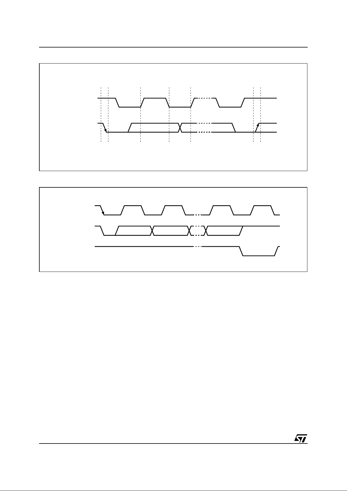
Bus not busy. Both data and clock li nes remain
High.
Start data transfer. A change in the s tate of the
data line, from High t o Low, while the c lock is High,
defines the START condition.
Stop data transfer. A c hange in the state of the
data line, from Low to High, while the clock is High,
defines the STOP condition.
Data Valid. T he state of the data line rep resents
valid data when after a start condition, the data line
is stable for the duration of the high period of the
clock signal. The data on the line may be changed
during the Low period of the clock signal. There is
one clock pulse per bit of data.
Each data transfer is initiated with a start condition
and terminated with a stop condition. The number
of data bytes transferred between the start and
stop conditions is not limited. The information is
transmitted byte-wide and each receiver acknowledges with a ninth bit.
By definition a device that gives o ut a m essag e is
called “transmitter”, the receiving device that gets
the message is called “rec eiver”. The device that
controls the message is called “master”. T he devices that are controlled by the master are cal led
“slaves”.
Acknowledge. E ac h byte of eight bits is followed
by one Acknowledge Bit. This Acknowledge Bit is
a low level put on the bus by the receiver whereas
the master generates an extra acknowledge relat-
.
ed clock pulse. A slave receiver which is addressed is obliged to generate an acknowledge
after the reception of each byte that has been
clocked out of the slave transmitter.
The device that acknowledges has to pull down
the SDA line during the acknowledge clock pulse
in such a way that the SDA line is a stable Low during the High period of the acknowledge related
clock pulse. Of course, setup and hold times must
be taken into account. A master receiver must signal an end of data to the slave transm itter by not
generating an acknowledge on the last byte that
has been clocked out of the slave. In this case the
transmitter must leave the data line High to enable
the master to generate the STOP condition.
7/31
M41ST84Y, M41ST84W
Figure 8. Serial Bus Data Transfer Sequence
DATA LINE
STABLE
DATA VALID
CLOCK
DATA
START
CONDITION
Figure 9. Acknowledgement Sequence
START
SCLK FROM
MASTER
DATA OUTPUT
BY TRANSMITTER
DATA OUTPUT
BY RECEIVER
12 89
MSB LSB
CHANGE OF
DATA ALLOWED
STOP
CONDITION
AI00587
CLOCK PULSE FOR
ACKNOWLEDGEMENT
AI00601
8/31
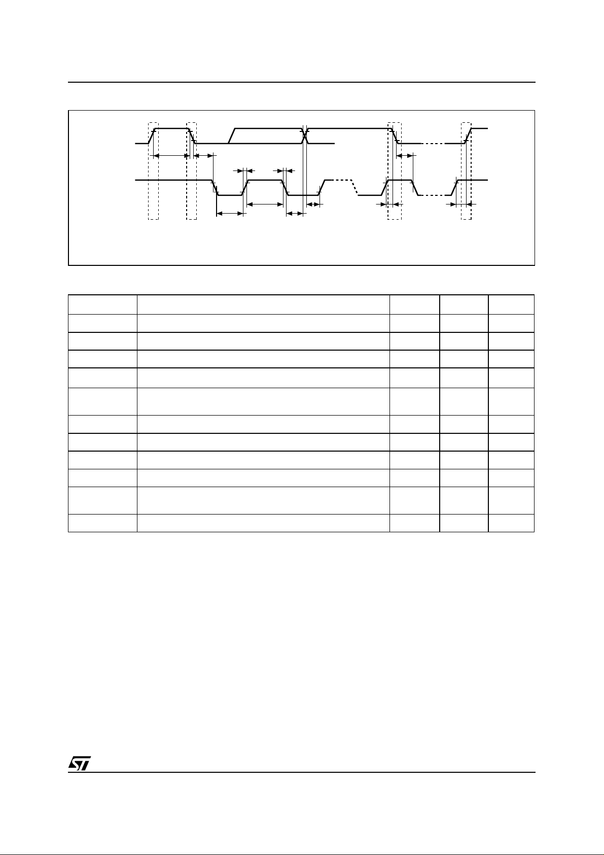
Figure 10. Bus Timing Requirements Sequence
SDA
M41ST84Y, M41ST84W
tHD:STA
P
AI00589
SCL
tHD:STAtBUF
tHIGH
tLOW
tF
tSU:DAT
tHD:DAT
SR
tR
SP
Table 2. AC Characteristics
Symbol
f
SCL
t
BUF
t
F
t
HD:DAT
t
HD:STA
t
HIGH
t
LOW
t
R
t
SU:DAT
t
SU:STA
t
SU:STO
Note: 1. Vali d for Ambient Op erating Temperature: TA = –40 to 85°C; VCC = 2.7 to 3.6V or 4. 5 to 5.5V (except where noted).
2. Transmitter must internal l y provide a hold time to brid ge t he undefined region (300ns max) of the fa lli ng edge of SCL.
SCL Clock Frequency 0 400 kHz
Time the bus must be free before a new transmission can start 1.3 µs
SDA and SCL Fall Time 300 ns
(2)
Data Hold Time 0 µs
START Condition Hold Time
(after this period the first clock pulse is generated)
Clock High Period 600 ns
Clock Low Period 1.3 µs
SDA and SCL Rise Time 300 ns
Data Setup Time 100 ns
START Condition Setup Time
(only relevant for a repeated start condition)
STOP Condition Setup Time 600 ns
Parameter
(1)
Min Max Unit
600 ns
600 ns
tSU:STOtSU:STA
9/31
M41ST84Y, M41ST84W
READ Mode
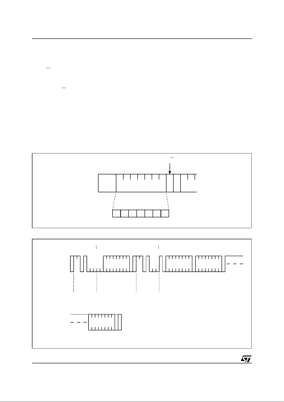
In this mode the master reads the M 41ST84Y/W
slave after setting the slave address (see Figure
11., page 10). Following the WRITE Mode Control
Bit (R/W
address ‘An’ is written to the on-chip address
pointer. Next the START condition and slave address are repeated followed by the READ Mode
Control Bit (R/W
mitter becomes the master receiver. The data byte
which was addressed will be transmitted and the
master receiver will send an A cknowledge Bit to
the slave transmitter. The address pointe r is only
incremented on reception of an Acknowledge
Clock. The M41ST84Y/W slave transmitter will
now place the data byte at address An+1 on the
bus, the master receiver reads and acknowledges
the new byte and the address pointer is
incremented to “An+2.”
Figure 11. Slave Address Location
=0) and the Acknowledge Bit, the word
=1). At this point the master trans-
This cycle of reading con secutive addresses will
continue until the master rec eiver sends a STOP
condition to the slave transmitter (see Figure
12., page 10).
The system-to-user transfer of clock data will be
halted whenever the address being read is a clock
address (00h to 07h). The update will resum e either due to a Stop Condition or when the pointer
increments to a non-clock or RAM address.
Note: This is true both in READ Mode and WRITE
Mode.
An alternate READ Mode may also be implemented whereby the master reads the M41ST84Y/W
slave without first writing to the (volatile) addres s
pointer. The first address that is read is the l ast
one stored in the pointer (see Figure
13., page 11).
R/W
START A
Figure 12. RE A D Mo de S equence
BUS ACTIVITY:
MASTER
SDA LINE
BUS ACTIVITY:
START
S
ADDRESS
R/W
SLAVE
DATA n+X
MSB
WORD
ADDRESS (An)
ACK
STOP
P
SLAVE ADDRESS
0100011
START
S
ACK
SLAVE
ADDRESS
LSB
AI00602
R/W
DATA n DATA n+1
ACK
ACK
ACK
10/31
AI00899
NO ACK
 Loading...