

ST M36L0R7050T0, M36L0R7050B0 User Manual
查询M36L0R7050供应商
128 Mbit (Multiple Bank, Multi-Level, Burst) Flash Memory
32 Mbit (2M x16) PSRAM, 1.8V Supply Multi-Chip Package
FEATURES SUMMARY
■ MULTI-CHIP PACKAGE
– 1 die of 128 Mbit (8Mb x16, Multiple Bank,
Multi-level, Burst) Flash Memory
– 1 die of 32 Mbit (2Mb x16) Asynchronous
Pseudo SRAM
■ SUPPLY VOLTAGE
–V
–V
■ ELECTRONIC SIGNATURE
= V
DDF
= 9V for fast program (12V tolerant)
PPF
– Manufacturer Code: 20h
– Device Code (Top Flash Configuration)
M36L0R7050T0: 88C4h
– Device Code (Bottom Flas h
Configuration) M36L0R7050B0: 88C5h
■ PACKAGE
– Compliant with Lead-Free Soldering
Processes
– Lead-Free Versions
FLASH MEMORY
■ SYNCHRONOUS / ASYNCHRONOUS READ
– Synchronous Burst Read mode: 54MHz
– Asynchronous Page Read mode
– Random Access: 85ns
■ SYNCHRONOUS BURST READ SUSPEND
■ PROGRAMMING TIME
– 10µs typical Word program time using
Buffer Program
■ MEMORY ORGANIZATION
– Multiple Bank Memory Array: 8 Mbit
Banks
– Parameter Blocks (Top or Bottom
location)
■ DUAL OPERATIONS
– program/erase in one Ban k whi le read in
others
– No delay between read and write
operations
■ SECURITY
– 64 bit unique device number
– 2112 bit user programmable OTP Cells
DDP
= V
= 1.7 to 1.95V
DDQ
M36L0R7050T0
M36L0R7050B0
Figure 1. Package
FBGA
TFBGA88 (ZAQ)
8 x 10mm
■ BLOCK LOCKING
– All blocks lock ed at power -up
– Any combination of blocks can be locked
with zero latency
–WP
– Absolute Write Protection with V
■ COMMON FLASH INTERFACE (CFI)
■ 100,000 PROGRAM/ERASE CYCLES per
BLOCK
PSRAM
■ ACCESS TIME: 85ns
■ LOW STANDBY CURRENT: 100µA
■ DEEP POWER-DOWN CURRENT: 10µA
■ BYTE CONTROL: UB
■ PROGRAMMABLE PARTIAL ARRAY
■ 8 WORD PAGE ACCESS CAPABILITY: 25ns
■ PARTIAL POWER-DOWN MODES
– Deep Power-Down
– 4 Mbit Partial Power-Down
– 8 Mbit Partial Power-Down
– 16 Mbit Partial Power-Down
for Block Lock-Down
F
/LB
P
= V
PPF
P
SS
1/18December 2004

M36L0R7050T0, M36L0R7050B0
TABLE OF CONTENTS
FEATURES SUMMARY . . . . . . . . . . . . . . . . . . . . . . . . . . . . . . . . . . . . . . . . . . . . . . . . . . . . . . . . . . . . . 1
FLASH MEMORY . . . . . . . . . . . . . . . . . . . . . . . . . . . . . . . . . . . . . . . . . . . . . . . . . . . . . . . . . . . . . . . 1
Figure 1. Package. . . . . . . . . . . . . . . . . . . . . . . . . . . . . . . . . . . . . . . . . . . . . . . . . . . . . . . . . . . . . . . 1
PSRAM . . . . . . . . . . . . . . . . . . . . . . . . . . . . . . . . . . . . . . . . . . . . . . . . . . . . . . . . . . . . . . . . . . . . . . . 1
SUMMARY DESCRIPTION. . . . . . . . . . . . . . . . . . . . . . . . . . . . . . . . . . . . . . . . . . . . . . . . . . . . . . . . . . . 4
Figure 2. Logic Diagram . . . . . . . . . . . . . . . . . . . . . . . . . . . . . . . . . . . . . . . . . . . . . . . . . . . . . . . . . . 4
Table 1. Signal Names . . . . . . . . . . . . . . . . . . . . . . . . . . . . . . . . . . . . . . . . . . . . . . . . . . . . . . . . . . 4
Figure 3. TFBGA Connections (Top view through package) . . . . . . . . . . . . . . . . . . . . . . . . . . . . . . 5
SIGNAL DESCRIPTIONS . . . . . . . . . . . . . . . . . . . . . . . . . . . . . . . . . . . . . . . . . . . . . . . . . . . . . . . . . . . . 6
Address Inputs (A0-A22). . . . . . . . . . . . . . . . . . . . . . . . . . . . . . . . . . . . . . . . . . . . . . . . . . . . . . . . . . 6
Data Input/Output (DQ0-DQ15). . . . . . . . . . . . . . . . . . . . . . . . . . . . . . . . . . . . . . . . . . . . . . . . . . . . . 6
Flash Chip Enable (E
Flash Output Enable (G
Flash Write Enable (W
Flash Write Protect (WP
Flash Reset (RP
Flash Latch Enable (L
Flash Clock (K
F
Flash Wait (WAIT
PSRAM Chip Enable (E1
PSRAM Chip Enable (E2
PSRAM Output Enable (G
PSRAM Write Enable (W
PSRAM Upper Byte Enable (UB
PSRAM Lower Byte Enable (LB
V
Supply Voltage . . . . . . . . . . . . . . . . . . . . . . . . . . . . . . . . . . . . . . . . . . . . . . . . . . . . . . . . . . . . . 7
DDF
V
Supply Voltage. . . . . . . . . . . . . . . . . . . . . . . . . . . . . . . . . . . . . . . . . . . . . . . . . . . . . . . . . . . . . 7
DDP
Supply Voltage. . . . . . . . . . . . . . . . . . . . . . . . . . . . . . . . . . . . . . . . . . . . . . . . . . . . . . . . . . . . . 7
V
DDQ
V
Program Supply Voltage. . . . . . . . . . . . . . . . . . . . . . . . . . . . . . . . . . . . . . . . . . . . . . . . . . . . . . 7
PPF
Ground.. . . . . . . . . . . . . . . . . . . . . . . . . . . . . . . . . . . . . . . . . . . . . . . . . . . . . . . . . . . . . . . . . . . . 7
V
SS
).. . . . . . . . . . . . . . . . . . . . . . . . . . . . . . . . . . . . . . . . . . . . . . . . . . . . . . . . . . . 6
F
).. . . . . . . . . . . . . . . . . . . . . . . . . . . . . . . . . . . . . . . . . . . . . . . . . . . . . . . . . 6
F
).. . . . . . . . . . . . . . . . . . . . . . . . . . . . . . . . . . . . . . . . . . . . . . . . . . . . . . . . . . 6
F
). . . . . . . . . . . . . . . . . . . . . . . . . . . . . . . . . . . . . . . . . . . . . . . . . . . . . . . . . 6
F
). . . . . . . . . . . . . . . . . . . . . . . . . . . . . . . . . . . . . . . . . . . . . . . . . . . . . . . . . . . . . . . 6
F
). . . . . . . . . . . . . . . . . . . . . . . . . . . . . . . . . . . . . . . . . . . . . . . . . . . . . . . . . . . 6
F
). . . . . . . . . . . . . . . . . . . . . . . . . . . . . . . . . . . . . . . . . . . . . . . . . . . . . . . . . . . . . . . . .6
).. . . . . . . . . . . . . . . . . . . . . . . . . . . . . . . . . . . . . . . . . . . . . . . . . . . . . . . . . . . . . . 6
F
).. . . . . . . . . . . . . . . . . . . . . . . . . . . . . . . . . . . . . . . . . . . . . . . . . . . . . . . . 6
P
).. . . . . . . . . . . . . . . . . . . . . . . . . . . . . . . . . . . . . . . . . . . . . . . . . . . . . . . . 6
P
).. . . . . . . . . . . . . . . . . . . . . . . . . . . . . . . . . . . . . . . . . . . . . . . . . . . . . . . 7
P
).. . . . . . . . . . . . . . . . . . . . . . . . . . . . . . . . . . . . . . . . . . . . . . . . . . . . . . . . 7
P
). . . . . . . . . . . . . . . . . . . . . . . . . . . . . . . . . . . . . . . . . . . . . . . . . . . 7
P
). . . . . . . . . . . . . . . . . . . . . . . . . . . . . . . . . . . . . . . . . . . . . . . . . . . 7
P
FUNCTIONAL DESCRIPTION . . . . . . . . . . . . . . . . . . . . . . . . . . . . . . . . . . . . . . . . . . . . . . . . . . . . . . . . 8
Figure 4. Functional Block Diagram . . . . . . . . . . . . . . . . . . . . . . . . . . . . . . . . . . . . . . . . . . . . . . . . . 8
Table 2. Main Operating Modes . . . . . . . . . . . . . . . . . . . . . . . . . . . . . . . . . . . . . . . . . . . . . . . . . . . 9
FLASH MEMORY DEVICE . . . . . . . . . . . . . . . . . . . . . . . . . . . . . . . . . . . . . . . . . . . . . . . . . . . . . . . . . . 10
PSRAM DEVICE . . . . . . . . . . . . . . . . . . . . . . . . . . . . . . . . . . . . . . . . . . . . . . . . . . . . . . . . . . . . . . . . . . 10
Table 3. Power-Down Configuration Data. . . . . . . . . . . . . . . . . . . . . . . . . . . . . . . . . . . . . . . . . . . 10
MAXIMUM RATING. . . . . . . . . . . . . . . . . . . . . . . . . . . . . . . . . . . . . . . . . . . . . . . . . . . . . . . . . . . . . . . . 11
2/18

M36L0R7050T0, M36L0R7050B0
Table 4. Absolute Maximum Ratings. . . . . . . . . . . . . . . . . . . . . . . . . . . . . . . . . . . . . . . . . . . . . . . 11
DC AND AC PARAMETERS. . . . . . . . . . . . . . . . . . . . . . . . . . . . . . . . . . . . . . . . . . . . . . . . . . . . . . . . . 12
Table 5. Operating and AC Measurement Conditions. . . . . . . . . . . . . . . . . . . . . . . . . . . . . . . . . . 12
Figure 5. AC Measurement I/O Waveform . . . . . . . . . . . . . . . . . . . . . . . . . . . . . . . . . . . . . . . . . . . 12
Figure 6. AC Measurement Load Circuit. . . . . . . . . . . . . . . . . . . . . . . . . . . . . . . . . . . . . . . . . . . . . 12
Table 6. Device Capacitance. . . . . . . . . . . . . . . . . . . . . . . . . . . . . . . . . . . . . . . . . . . . . . . . . . . . . 12
Table 7. Flash Memory DC Characteristics - Currents . . . . . . . . . . . . . . . . . . . . . . . . . . . . . . . . . 13
Table 8. Flash Memory DC Characteristics - Voltages . . . . . . . . . . . . . . . . . . . . . . . . . . . . . . . . . 14
Table 9. PSRAM DC Characteristics . . . . . . . . . . . . . . . . . . . . . . . . . . . . . . . . . . . . . . . . . . . . . . 14
PACKAGE MECHANICAL . . . . . . . . . . . . . . . . . . . . . . . . . . . . . . . . . . . . . . . . . . . . . . . . . . . . . . . . . . 15
Figure 7. Stacked TFBGA88 8x10mm - 8x10 active ball array, 0.8mm pitch, Bottom View Outline15
Table 10. Stacked TFBGA88 8x10mm - 8x10 active ball array, 0.8mm pitch, Package Data. . . . . 15
PART NUMBERING . . . . . . . . . . . . . . . . . . . . . . . . . . . . . . . . . . . . . . . . . . . . . . . . . . . . . . . . . . . . . . . 16
Table 11. Ordering Information Scheme . . . . . . . . . . . . . . . . . . . . . . . . . . . . . . . . . . . . . . . . . . . . . 16
REVISION HISTORY. . . . . . . . . . . . . . . . . . . . . . . . . . . . . . . . . . . . . . . . . . . . . . . . . . . . . . . . . . . . . . . 17
Table 12. Document Revision History . . . . . . . . . . . . . . . . . . . . . . . . . . . . . . . . . . . . . . . . . . . . . . . 17
3/18
M36L0R7050T0, M36L0R7050B0
SUMMARY DESCRIPTION
The M36L0R7050T0 and M36L0R7050B0 combine two memory devices in a Multi-Chip Package:
a 128-Mbit, Multiple Bank Flash memory, the
M30L0R7000T0 or M30L0R7000B0, and a 32Mbit PseudoSRAM, the M69AR048B. Recommended operating conditions do not allow more
than one memory to be active at the same time.
The memory is offered in a Stacked TFBGA88
(8x10mm, 8x10 ball array, 0.8mm pitch) package.
In addition to the stan dard version, the pac kages
are also available in Lead- free version , in comp liance with JEDEC Std J-STD-020 B, the ST ECOPACK 7191395 Specification, and the RoHS
(Restriction of Hazardous Substances) directive.
All packages are c omp lia nt with Le ad- fr ee so ld er ing processes.
The memory is supplied with all the bits erased
(set to ‘1’).
Table 1. Signal Names
A0-A22
(1)
DQ0-DQ15 Common Data Input/Output
V
DDF
V
DDQ
V
PPF
V
SS
V
DDP
NC Not Connected Internally
DU Do Not Use as Internally Connected
Address Inputs
Power Supply for Flash Memory
Flash Memory Power Supply for I/O
Buffers
Flash Optional Supply Voltage for Fast
Program and Erase
Ground
PSRAM Power Supply
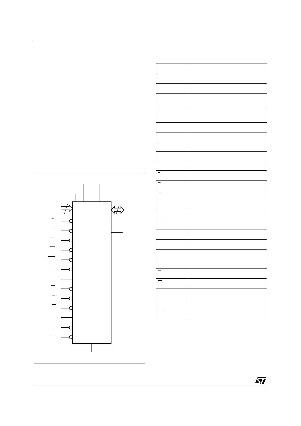
Figure 2. Logic Diagram
V
DDQ
V
DDF
23
A0-A22
E
F
G
F
W
F
RP
F
WP
E1
E2
UB
LB
G
W
F
L
F
K
F
P
P
P
P
P
P
M36L0R7050T0
M36L0R7050B0
Flash Memory
L
V
PPF
V
DDP
16
DQ0-DQ15
WAIT
F
F
E
F
G
F
W
F
RP
F
WP
K
F
WAIT
F
F
Latch Enable Input
Chip Enable Input
Output Enable Input
Write Enable Input
Reset Input
Write Protect Input
Burst Clock
Wait Data in Burst Mode
PSRAM
E1
P
G
P
W
P
E2
P
UB
P
LB
P
Note: 1. A22-A21 are not connected to the PSRAM component.
Chip Enable Input
Output Enable Input
Write Enable Input
Power-down Input
Upper Byte Enable Inp ut
Lower Byte Enable Inp ut
4/18
V
SS
AI08731
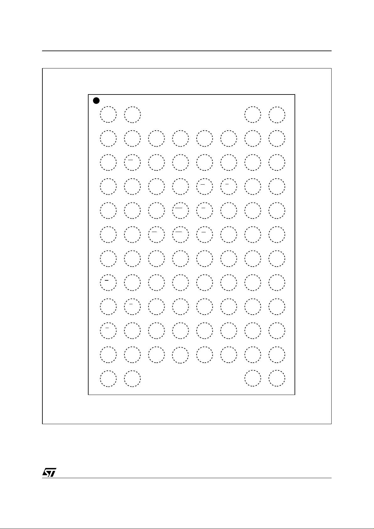
Figure 3. TFBGA Connections (Top view through package)
M36L0R7050T0, M36L0R7050B0
87654321
A
B A21
C
D
E
F
G
H
DU
A4
A5
A3
A2
A1
A0
G
DU
A19A18
LB
P
A6
P
NC
NCA17
NCA7
UB
DQ2DQ8
DQ1DQ0
V
SS
V
SS
V
PPF
WP
RP
P
DQ10
DQ3
V
DDF
NC
W
P
L
F
F
F
W
F
DQ5
DQ12
NC
K
F
E
P
DQ13
DU
A22
A9
A10A20
A14A8
WAIT
DQ7DQ14
DU
A11
A12
A13
A15
A16
NC
F
NC
J
K
L
M
V
NC
E
DU
SS
DQ9G
F
F
DU DU NC
V
SS
DU
V
DDQ
DQ11
V
DDF
V
V
DDP
SS
NC
V
SS
DQ15DQ6DQ4
V
V
DDQ
SS
DU
V
E2
V
DDQ
P
SS
DU
AI08732
5/18

M36L0R7050T0, M36L0R7050B0
SIGNAL DESCRIPTIONS
See Figure 2., Logic Diagram and Table 1., Signal
Names, for a brief overview of the signals connect-
ed to this device.
Address Inputs (A0-A22). Addresses A0-A20
are common inputs fo r th e Fl as h Mem ory an d the
PSRAM components. The other lines (A21-A22)
are inputs for the Flash Memory components only.
The Address Inputs select the cells in the memory
array to access during Bus Read operations. During Bus Write operations they control the commands sent to the Command Interface of the Flash
memory Program/Eras e Controller or they select
the cells to access in the PSRAM.
The Flash memory component is accessed
through the Chip Enable s ignal (E
the Write Enable (W
) signal, while the PSRAM is
F
accessed through two Chip E nable signals (E1
and E2P) and the Write Enable signal (WP).
Data Input/Output (DQ0-DQ15). In the Flash
memory the Data I/O outputs the data stored at the
selected address du ring a Bus Read operati on or
inputs a command or the data to be pro grammed
during a Write Bus operation.
In the PSRAM the Lower Byte Data Inputs/Outputs, DQ0-DQ7, carry the data to or from the lower
part of the selected address during a Write or
Read operation, when Lower Byte Enable (LB
driven Low.
The Upper Byte Data Inputs/Outputs, DQ8-DQ15,
carry the data to or from the upper part of the selected address dur ing a Write or Rea d operation,
when Upper Byte Enable (UB
Flash Chip Enable (E
). The Chip Enable input
F
activates the memory cont rol logic, input buffers,
decoders and sense amplifiers. When Chip Enable is Low, V
, and Reset is High, VIH, the device
IL
is in active mode. W hen Chi p E nab le i s at V
Flash memory is deselect ed, the out puts ar e high
impedance and the power consumption is reduced
to the standby level.
Flash Output Enable (G
). The Output Enable
F
input controls data output during Flash memory
Bus Read operations.
Flash Write Enable (
W
). The Write Enable
F
controls the Bus Write operation of the Flash
memories’ Command Int erface. The data an d address inputs are latched on the rising edge of Chip
Enable or Write Enable whichever occurs first.
Flash Write Protect (WP
). Write Protect is an
F
input that gives an additio nal hardware protection
for each block. When Write Protect is Low, V
Lock-Down is enabled and the protection status of
the Locked-Down blocks cannot be changed.
When Write Protect is a t High, V
disabled and the Locked-Down blocks can be
) and through
F
) is driven Low.
P
, Lock-Down is
IH
IH
) is
P
the
IL
locked or unlocked. (See the Lock Status Table in
the M30L0R7000T0 datasheet).
Flash Reset (RP
). The Reset input prov ides a
F
hardware reset of the m emory. When Reset is at
, the memory is in Reset mode: the outputs are
V
IL
high impedance and the current consumption is
reduced to the Reset Supply Current I
Table 7.,Flash Memory DC Characteristics - Currents, for th e value o f I
. After Reset all b locks
DD2
are in the Locked state and the Configuration Register is reset. When Reset is at V
, the device is in
IH
normal operation. Exiti ng Reset mode the devic e
enters Asynchronous Read mode, but a nega tive
transition of Chip Enable or Latch Enable is required to ensure valid data outputs.
The Reset pin can be interfaced with 3V logic without any additional circui try. It can be tied to V
P
(refer to Table 8., Flash Memory DC Characteris-
tics - Voltages).
Flash Latch Enable (L
). Latch Enable latches
F
the address bits on its rising edge. The address
latch is transparent when Latch Enable is Low, V
and it is inhibited when Latch Enable i s H igh , V
Latch Enable can be kept Low (also at board level)
when the Latch Enable func tion is not requ ired or
supported.
Flash Clock (K
). The Clock input sy nchronizes
F
the Flash memory to the microcontroller during
synchronous read operations; the address is
latched on a Clock edge (r ising o r falling, according to the configurat ion settings) when Latch En able is at V
. Clock is don't care during
IL
Asynchronous Read and in write operations.
Flash Wait (WAIT
). WAIT is a Flash output sig-
F
nal used during Synchronous Read to indicate
whether the data on the output bus are valid. This
output is high impedance when Flash Chip Enable
is at V
or Flash Reset is at VIL. It can be config-
IH
ured to be active during the wait cycle or one clock
cycle in advance. The WA IT
signal is not gated
F
by Output Enable.
PSRAM Chip Enable (E1
(Low), the Chip Enable, E1
). When asserted
P
, activates the memo-
P
ry state machine, address buffers and decod ers,
allowing Read and Write operations to be performed. When de-asserted (High), all other pins
are ignored, and the device is put, automatically, in
low-power Standby mode.
It is not allowed to set E
at V
at the same time.
IH
PSRAM Chip Enable (E2
,
, puts the device in Power-down mode (Deep
E2
P
at V
F
E1P at VIL and E2
IL,
). The Chip Enable,
P
Power-Down or a Partial Power-Down mode)
when it is drive n Low. De ep Po wer- down m ode i s
the lowest power mode.
DD2
. Refer to
RPH
IL
IH
,
.
P
6/18
 Loading...