

Page 1
32 Kbit, 256-byte page, fast program EEPROM memory
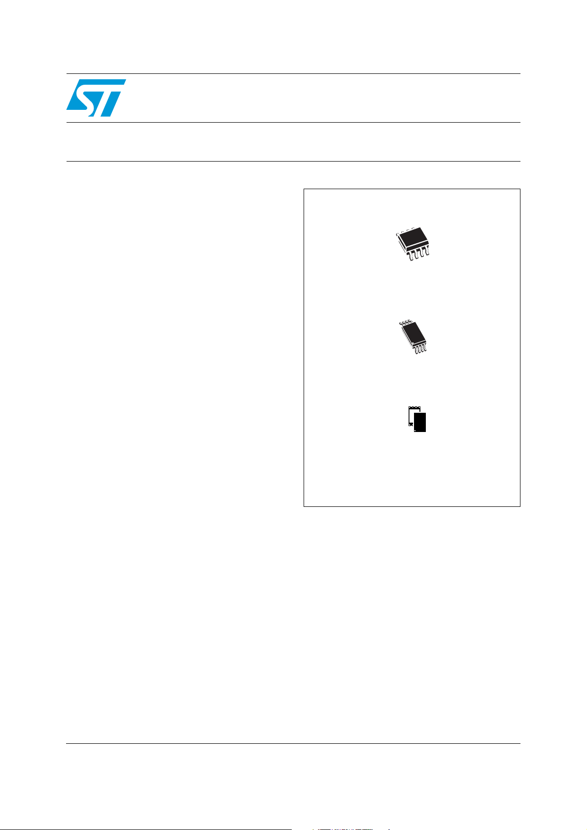
SO8 (MN)
150 mil width
TSSOP8 (DW)
169 mil width
UFDFPN8 (MC)
2 x 3 mm
Features
■ SPI bus compatible serial interface
■ 32 Kbit of EEPROM divided into two sectors:
– Data sector
– Event sector
■ Large page size: 256 bytes
■ Fast programming:
– Event sector: 256 bytes programmed in
less than 1 ms
– Data sector: 256 bytes written in less than
5ms
■ Low energy EEPROM in either Read, Write,
Program or Erase modes
■ 2.5 V to 5.5 V single supply voltage
■ Operating temperature range:
– –40°C to +85°C
– –40°C to +125°C
■ Operating frequency, f
■ Electronic signature: 20 10 0Ch
■ Data cycling:
– Data sector: more than 1 Million write
cycles
– Event sector: more than 10 000 write
cycles
■ Data retention:
– Data sector: more than 40 years’ data
retention
– Event sector: 1 year
■ Packages
–ECOPACK
® (RoHS compliant)
= 20 MHz
C
M35B32
accessed by SPI bus interface
Target specification
May 2011 Doc ID 18391 Rev 3 1/42
This is preliminary information on a new product foreseen to be developed. Details are subject to change without notice.
www.st.com
1
Page 2

Contents M35B32
Contents
1 Description . . . . . . . . . . . . . . . . . . . . . . . . . . . . . . . . . . . . . . . . . . . . . . . . . 6
2 Signal description . . . . . . . . . . . . . . . . . . . . . . . . . . . . . . . . . . . . . . . . . . . 8
2.1 Serial Data output (Q) . . . . . . . . . . . . . . . . . . . . . . . . . . . . . . . . . . . . . . . . 8
2.2 Serial Data input (D) . . . . . . . . . . . . . . . . . . . . . . . . . . . . . . . . . . . . . . . . . . 8
2.3 Serial Clock (C) . . . . . . . . . . . . . . . . . . . . . . . . . . . . . . . . . . . . . . . . . . . . . 8
2.4 Chip Select (S
2.5 Reset (RESET
2.6 Write Protect (W
2.7 V
2.8 V
supply voltage . . . . . . . . . . . . . . . . . . . . . . . . . . . . . . . . . . . . . . . . . . . 9
CC
ground . . . . . . . . . . . . . . . . . . . . . . . . . . . . . . . . . . . . . . . . . . . . . . . . . 9
SS
) . . . . . . . . . . . . . . . . . . . . . . . . . . . . . . . . . . . . . . . . . . . . . . 8
) . . . . . . . . . . . . . . . . . . . . . . . . . . . . . . . . . . . . . . . . . . . . . . 8
) . . . . . . . . . . . . . . . . . . . . . . . . . . . . . . . . . . . . . . . . . . . . 9
3 SPI modes . . . . . . . . . . . . . . . . . . . . . . . . . . . . . . . . . . . . . . . . . . . . . . . . 10
4 Operating features . . . . . . . . . . . . . . . . . . . . . . . . . . . . . . . . . . . . . . . . . 12
4.1 An easy way to modify data . . . . . . . . . . . . . . . . . . . . . . . . . . . . . . . . . . . 12
4.2 A fast way to store data . . . . . . . . . . . . . . . . . . . . . . . . . . . . . . . . . . . . . . 12
4.3 Polling during a write, program or erase cycle . . . . . . . . . . . . . . . . . . . . . 12
4.4 Protection modes . . . . . . . . . . . . . . . . . . . . . . . . . . . . . . . . . . . . . . . . . . . 13
5 Memory organization . . . . . . . . . . . . . . . . . . . . . . . . . . . . . . . . . . . . . . . 14
6 Instructions . . . . . . . . . . . . . . . . . . . . . . . . . . . . . . . . . . . . . . . . . . . . . . . 16
6.1 Write Enable (WREN) . . . . . . . . . . . . . . . . . . . . . . . . . . . . . . . . . . . . . . . 17
6.2 Write Disable (WRDI) . . . . . . . . . . . . . . . . . . . . . . . . . . . . . . . . . . . . . . . . 17
6.3 Read Identification (RDID) . . . . . . . . . . . . . . . . . . . . . . . . . . . . . . . . . . . . 18
6.4 Read Status Register (RDSR) . . . . . . . . . . . . . . . . . . . . . . . . . . . . . . . . . 19
6.4.1 WIP bit . . . . . . . . . . . . . . . . . . . . . . . . . . . . . . . . . . . . . . . . . . . . . . . . . . 19
6.4.2 WEL bit . . . . . . . . . . . . . . . . . . . . . . . . . . . . . . . . . . . . . . . . . . . . . . . . . 19
6.4.3 BPi bits . . . . . . . . . . . . . . . . . . . . . . . . . . . . . . . . . . . . . . . . . . . . . . . . . . 20
6.5 Write Status Register (WRSR) . . . . . . . . . . . . . . . . . . . . . . . . . . . . . . . . . 21
6.6 Read Data Bytes (READ) . . . . . . . . . . . . . . . . . . . . . . . . . . . . . . . . . . . . . 22
6.7 Page Write (PW) . . . . . . . . . . . . . . . . . . . . . . . . . . . . . . . . . . . . . . . . . . . 23
2/42 Doc ID 18391 Rev 3
Page 3

M35B32 Contents
6.8 Page Program (PP) . . . . . . . . . . . . . . . . . . . . . . . . . . . . . . . . . . . . . . . . . 25
6.9 ECC (error correction code) and write cycling . . . . . . . . . . . . . . . . . . . . . 26
6.10 Page Erase (PE) . . . . . . . . . . . . . . . . . . . . . . . . . . . . . . . . . . . . . . . . . . . 27
6.11 Sector Erase (SE) . . . . . . . . . . . . . . . . . . . . . . . . . . . . . . . . . . . . . . . . . . 28
7 Power-up and power-down . . . . . . . . . . . . . . . . . . . . . . . . . . . . . . . . . . . 29
7.1 Supply voltage (VCC) . . . . . . . . . . . . . . . . . . . . . . . . . . . . . . . . . . . . . . . . 29
7.1.1 Operating supply voltage V
7.1.2 Power-up conditions . . . . . . . . . . . . . . . . . . . . . . . . . . . . . . . . . . . . . . . 29
7.1.3 Internal reset during power up . . . . . . . . . . . . . . . . . . . . . . . . . . . . . . . . 29
7.1.4 Power-down . . . . . . . . . . . . . . . . . . . . . . . . . . . . . . . . . . . . . . . . . . . . . . 30
CC . . . . . . . . . . . . . . . . . . . . . . . . . . . . . . . . . . . . . . . . . 29
8 Initial delivery state . . . . . . . . . . . . . . . . . . . . . . . . . . . . . . . . . . . . . . . . . 31
9 Maximum rating . . . . . . . . . . . . . . . . . . . . . . . . . . . . . . . . . . . . . . . . . . . . 31
10 DC and AC parameters . . . . . . . . . . . . . . . . . . . . . . . . . . . . . . . . . . . . . . 32
11 Package mechanical data . . . . . . . . . . . . . . . . . . . . . . . . . . . . . . . . . . . . 37
12 Part numbering . . . . . . . . . . . . . . . . . . . . . . . . . . . . . . . . . . . . . . . . . . . . 40
13 Revision history . . . . . . . . . . . . . . . . . . . . . . . . . . . . . . . . . . . . . . . . . . . 41
Doc ID 18391 Rev 3 3/42
Page 4

List of tables M35B32
List of tables
Table 1. Signal names . . . . . . . . . . . . . . . . . . . . . . . . . . . . . . . . . . . . . . . . . . . . . . . . . . . . . . . . . . . . 7
Table 2. Instruction set . . . . . . . . . . . . . . . . . . . . . . . . . . . . . . . . . . . . . . . . . . . . . . . . . . . . . . . . . . . 16
Table 3. Read Identification (RDID) data-out sequence . . . . . . . . . . . . . . . . . . . . . . . . . . . . . . . . . . 18
Table 4. Value of the WEL bit after decoding a Page Write, Page Program, Page
Erase or Sector Erase instruction . . . . . . . . . . . . . . . . . . . . . . . . . . . . . . . . . . . . . . . . . . . . 19
Table 5. Absolute maximum ratings . . . . . . . . . . . . . . . . . . . . . . . . . . . . . . . . . . . . . . . . . . . . . . . . . 31
Table 6. Operating conditions (range 6) . . . . . . . . . . . . . . . . . . . . . . . . . . . . . . . . . . . . . . . . . . . . . . 32
Table 7. Operating conditions (range 3) . . . . . . . . . . . . . . . . . . . . . . . . . . . . . . . . . . . . . . . . . . . . . . 32
Table 8. AC measurement conditions. . . . . . . . . . . . . . . . . . . . . . . . . . . . . . . . . . . . . . . . . . . . . . . . 32
Table 9. Capacitance . . . . . . . . . . . . . . . . . . . . . . . . . . . . . . . . . . . . . . . . . . . . . . . . . . . . . . . . . . . . 32
Table 10. DC characteristics. . . . . . . . . . . . . . . . . . . . . . . . . . . . . . . . . . . . . . . . . . . . . . . . . . . . . . . . 33
Table 11. AC characteristics . . . . . . . . . . . . . . . . . . . . . . . . . . . . . . . . . . . . . . . . . . . . . . . . . . . . . . . . 34
Table 12. SO8N – 8-lead plastic small outline, 150 mils body width, mechanical data . . . . . . . . . . . 37
Table 13. TSSOP8 – 8-lead thin shrink small outline, package mechanical data. . . . . . . . . . . . . . . . 38
Table 14. UFDFPN8 (MLP8) 8-lead ultra thin fine pitch dual flat package no lead
2 x 3 mm, data . . . . . . . . . . . . . . . . . . . . . . . . . . . . . . . . . . . . . . . . . . . . . . . . . . . . . . . . . . 39
Table 15. Ordering information scheme . . . . . . . . . . . . . . . . . . . . . . . . . . . . . . . . . . . . . . . . . . . . . . . 40
Table 16. Document revision history . . . . . . . . . . . . . . . . . . . . . . . . . . . . . . . . . . . . . . . . . . . . . . . . . 41
4/42 Doc ID 18391 Rev 3
Page 5

M35B32 List of figures
List of figures
Figure 1. Logic diagram . . . . . . . . . . . . . . . . . . . . . . . . . . . . . . . . . . . . . . . . . . . . . . . . . . . . . . . . . . . . 6
Figure 2. 8-pin package connections . . . . . . . . . . . . . . . . . . . . . . . . . . . . . . . . . . . . . . . . . . . . . . . . . . 7
Figure 3. SPI modes supported . . . . . . . . . . . . . . . . . . . . . . . . . . . . . . . . . . . . . . . . . . . . . . . . . . . . . 10
Figure 4. Bus master and memory devices on the SPI bus. . . . . . . . . . . . . . . . . . . . . . . . . . . . . . . . 11
Figure 5. Memory organization . . . . . . . . . . . . . . . . . . . . . . . . . . . . . . . . . . . . . . . . . . . . . . . . . . . . . 14
Figure 6. Block diagram . . . . . . . . . . . . . . . . . . . . . . . . . . . . . . . . . . . . . . . . . . . . . . . . . . . . . . . . . . . 15
Figure 7. Write Enable (WREN) instruction sequence . . . . . . . . . . . . . . . . . . . . . . . . . . . . . . . . . . . . 17
Figure 8. Write Disable (WRDI) instruction sequence . . . . . . . . . . . . . . . . . . . . . . . . . . . . . . . . . . . . 17
Figure 9. Read Identification (RDID) instruction sequence and data-out sequence . . . . . . . . . . . . . 18
Figure 10. Read Status Register (RDSR) instruction sequence and data-out sequence . . . . . . . . . . 20
Figure 11. Write Status Register (WRSR) instruction sequence . . . . . . . . . . . . . . . . . . . . . . . . . . . . . 21
Figure 12. Read Data Bytes (READ) instruction sequence and data-out sequence . . . . . . . . . . . . . . 22
Figure 13. Page Write (PW) instruction sequence . . . . . . . . . . . . . . . . . . . . . . . . . . . . . . . . . . . . . . . . 24
Figure 14. Page Program (PP) instruction sequence . . . . . . . . . . . . . . . . . . . . . . . . . . . . . . . . . . . . . 26
Figure 15. Page Erase (PE) instruction sequence . . . . . . . . . . . . . . . . . . . . . . . . . . . . . . . . . . . . . . . . 27
Figure 16. Sector Erase (SE) instruction sequence . . . . . . . . . . . . . . . . . . . . . . . . . . . . . . . . . . . . . . . 28
Figure 17. AC measurement I/O waveform . . . . . . . . . . . . . . . . . . . . . . . . . . . . . . . . . . . . . . . . . . . . . 32
Figure 18. Serial input timing . . . . . . . . . . . . . . . . . . . . . . . . . . . . . . . . . . . . . . . . . . . . . . . . . . . . . . . . 35
Figure 19. Write Protect setup and hold timing . . . . . . . . . . . . . . . . . . . . . . . . . . . . . . . . . . . . . . . . . . 35
Figure 20. Output timing . . . . . . . . . . . . . . . . . . . . . . . . . . . . . . . . . . . . . . . . . . . . . . . . . . . . . . . . . . . 36
Figure 21. Reset AC waveforms . . . . . . . . . . . . . . . . . . . . . . . . . . . . . . . . . . . . . . . . . . . . . . . . . . . . . 36
Figure 22. SO8N – 8-lead plastic small outline, 150 mils body width, package outline. . . . . . . . . . . . 37
Figure 23. TSSOP8 – 8-lead thin shrink small outline, package outline . . . . . . . . . . . . . . . . . . . . . . . 38
Figure 24. Ultra thin Fine pitch Dual Flat Package No lead (UFDFPN8), 2 × 3mm
package outline. . . . . . . . . . . . . . . . . . . . . . . . . . . . . . . . . . . . . . . . . . . . . . . . . . . . . . . . . . 39
Doc ID 18391 Rev 3 5/42
Page 6
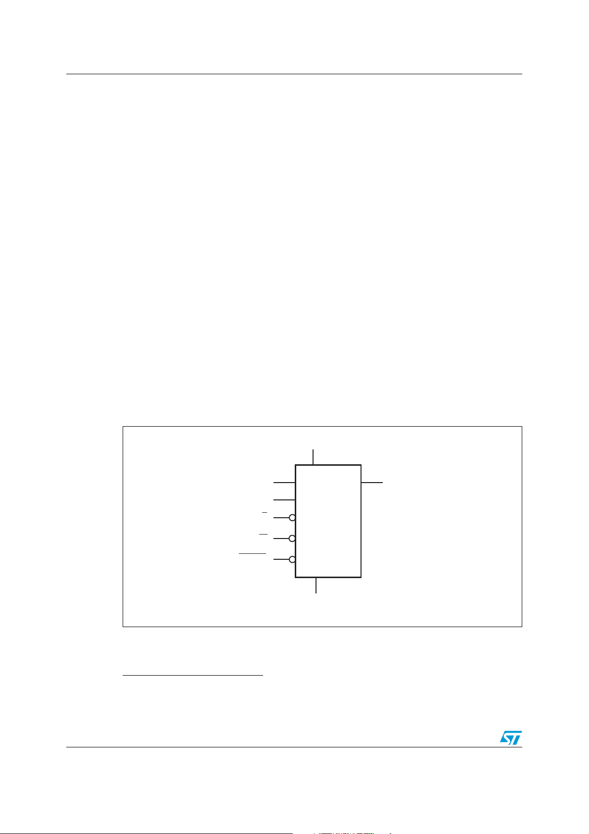
Description M35B32
RESET
AI15472
S
V
CC
M35B32
V
SS
W
Q
C
D
1 Description
The M35B32 is a 32-Kbit electrically erasable programmable memory (EEPROM) accessed
through the SPI bus.
The M35B32 is able to save and store up to 256 bytes within a very short time with the help
of the Event sector, this feature being convenient in cases of an unexpected power loss or if
an urgent data storage is required. The fast storage is performed with a very low energy
budget as the Program time lasts less than 1 ms and as the supply voltage can be as low as
2.5 V associated with a low Programming current (the M35B32 is based on EEPROM cells,
energy-saving technology when compared to the Flash technology).
Memory organization
The M35B32 is split into two sectors:
● the Data sector: standard EEPROM which can be written
a time) with a standard write time and a standard retention time,
● the Event sector: data bytes which can be programmed
time) with a fast programming time and a limited retention time.
The time required to update data is significantly reduced by the Page size (256 bytes) as a
page is updated in a single shot.
(a)
by page (1 to 256 bytes at
(b)
by page (1 to 256 bytes at a
Both Data sector and Event sector can be erased either a page at a time (using the Page
Erase instruction) or a sector at a time (using the Sector Erase instruction).
The size of each sector is defined by the user.
Figure 1. Logic diagram
a. Write cycle = 2 cycles = Erase + Program
b. Program cycle = single cycle (a Write cycle includes two cycles: Erase cycle + Program cycle)
6/42 Doc ID 18391 Rev 3
Page 7
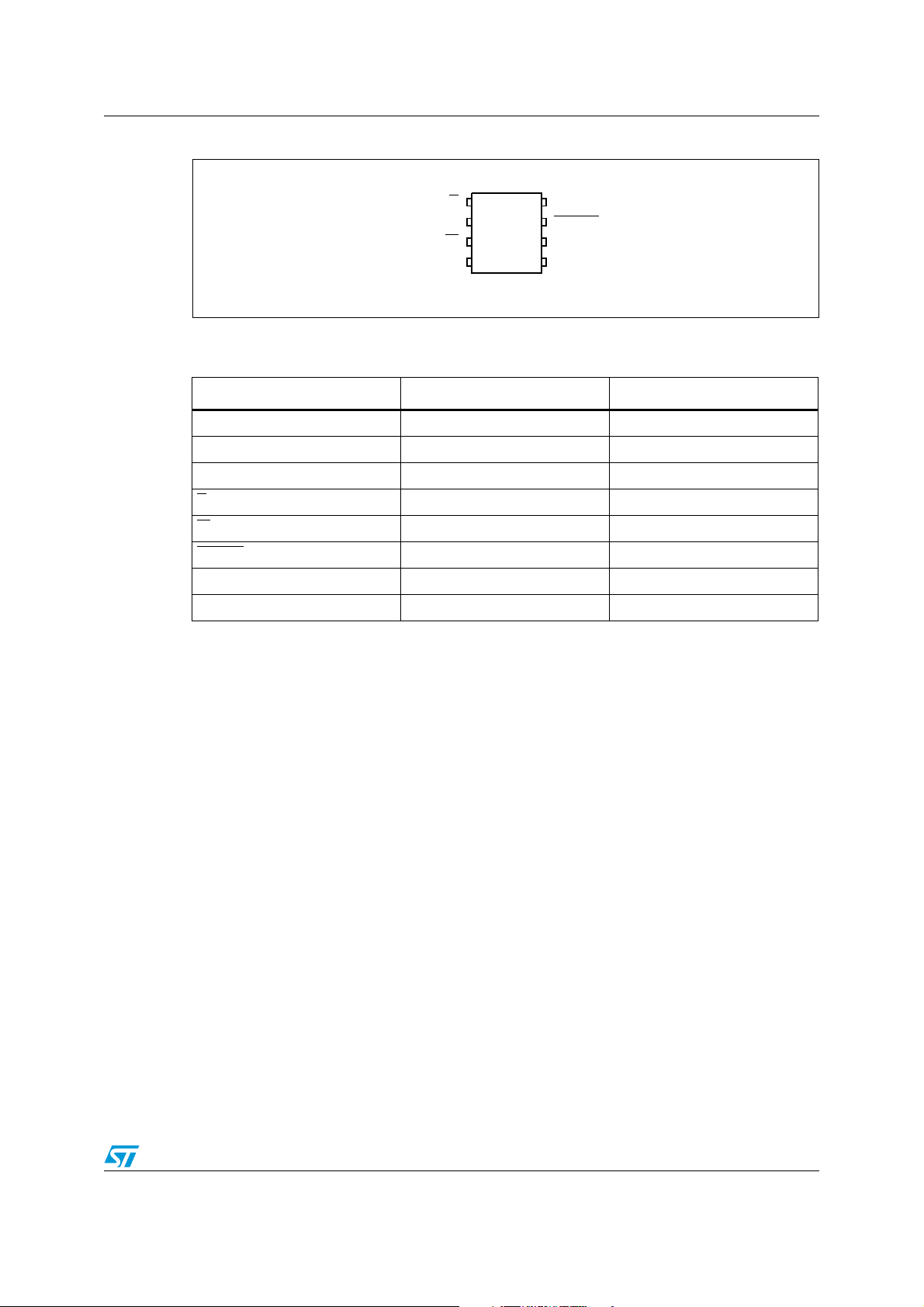
M35B32 Description
1
AI14872
2
3
4
8
7
6
5
RESET
DV
SS
C
Q
S
V
CC
W
Figure 2. 8-pin package connections
1. See Package mechanical data section for package dimensions, and how to identify pin-1.
Table 1. Signal names
Signal name Function Direction
C Serial Clock Input
D Serial Data input Input
Q Serial Data output Output
S Chip Select Input
W
RESET
Write Protect Input
Reset Input
V
CC
V
SS
Supply voltage
Ground
Doc ID 18391 Rev 3 7/42
Page 8

Signal description M35B32
2 Signal description
During all operations, VCC must be held stable and within the specified valid range:
V
(min) to VCC(max).
CC
All of the input and output signals must be held high or low (according to voltages of V
V
, VIL or VOL, as specified in Ta bl e 1 0 ). These signals are described below.
OH
2.1 Serial Data output (Q)
This output signal is used to transfer data serially out of the device. Data is shifted out on the
falling edge of Serial Clock (C).
2.2 Serial Data input (D)
This input signal is used to transfer data serially into the device. It receives instructions,
addresses, and the data to be programmed. Values are latched on the rising edge of Serial
Clock (C).
,
IH
2.3 Serial Clock (C)
This input signal provides the timing of the serial interface. Instructions, addresses, or data
present at Serial Data Input (D) are latched on the rising edge of Serial Clock (C). Data on
Serial Data Output (Q) changes after the falling edge of Serial Clock (C).
2.4 Chip Select (S)
When this input signal is high, the device is deselected and Serial Data Output (Q) is at high
impedance. Unless an internal Read, Program, Erase or Write cycle is in progress, the
device will be in the Standby Power mode (this is not the Deep Power-down mode). Driving
Chip Select (S
After Power-up, a falling edge on Chip Select (S
instruction.
) low selects the device, placing it in the Active Power mode.
2.5 Reset (RESET)
The Reset (RESET) input provides a hardware reset for the memory. In this mode, the
device is in Standby mode, the WEL and WIP bits are reset (to 0) and the outputs are high
impedance.
When Reset (RESET
Reset (RESET
) is driven high, the memory is in the normal operating mode. When
) is driven low, the memory will enter the Reset mode
) is required prior to the start of any
(c)
.
c. If the M35A32 is executing a Write (pr program) cycle), the RESET pin driven active (low) does not stop an on
going Program or Write cycle.
8/42 Doc ID 18391 Rev 3
Page 9

M35B32 Signal description
2.6 Write Protect (W)
This input signal puts the device in the Hardware Protected mode, when Write Protect (W) is
driven low (V
write, program and erase operations). When Write Protect (W
Kbytes of EEPROM memory can be accessed in Read and Write mode.
), causing the Event sector to become read-only (by protecting them from
IL
) is driven high (VIH), the 4
2.7 VCC supply voltage
VCC is the supply voltage. (See also Section 7 for more)
2.8 VSS ground
VSS is the reference for the VCC supply voltage.
Doc ID 18391 Rev 3 9/42
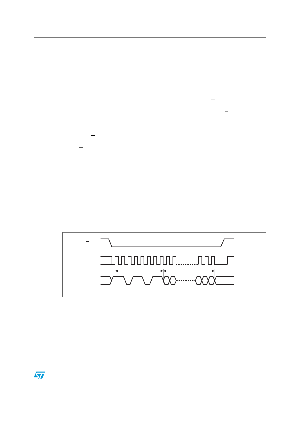
Page 10
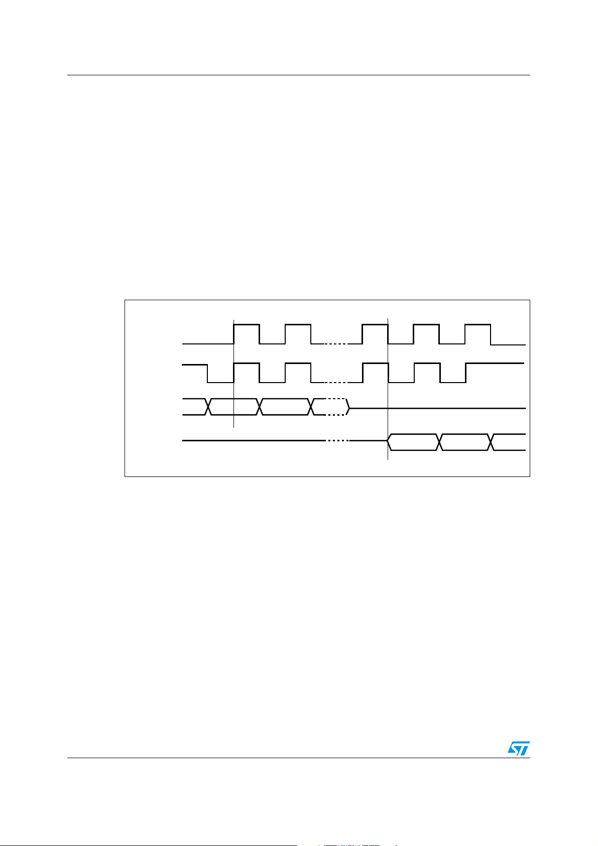
SPI modes M35B32
AI01438B
C
MSB
CPHA
D
0
1
CPOL
0
1
Q
C
MSB
3 SPI modes
These devices can be driven by a microcontroller with its SPI peripheral running in either of
the two following modes:
● CPOL=0, CPHA=0
● CPOL=1, CPHA=1
For these two modes, input data is latched in on the rising edge of Serial Clock (C), and
output data is available from the falling edge of Serial Clock (C).
The difference between the two modes, as shown in Figure 3, is the clock polarity when the
bus master is in Standby mode and not transferring data:
● C remains at 0 for (CPOL=0, CPHA=0)
● C remains at 1 for (CPOL=1, CPHA=1)
Figure 3. SPI modes supported
10/42 Doc ID 18391 Rev 3
Page 11
M35B32 SPI modes
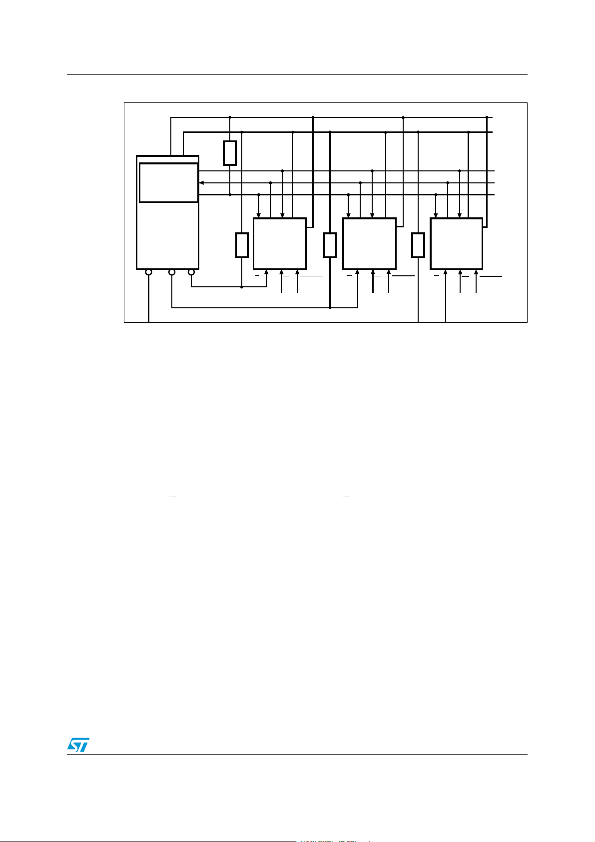
30)"US-ASTER
30)-EMORY
$EVICE
3$/
3$)
3#+
#1$
3
30)-EMORY
$EVICE
#1$
3
30)-EMORY
$EVICE
#1$
3
#3 #3 #3
30))NTERFACEWITH
#0/,#0(!
OR
7
2%3%4
7
2%3%4
7
2%3%4
22 2
6
##
6
##
6
##
6
##
6
33
6
33
6
33
6
33
2
2EFERTO.OTE 2EFERTO.OTE
2EFERTO.OTE
Figure 4. Bus master and memory devices on the SPI bus
Note: 1 The /W and /RESET inputs are CMOS inputs and have also to be driven high or low if/when the SPI
bus master leaves the lines in high impedance. This has to be done with the help of pull up or pull
down resistors (depending on the application requirements).
Figure 4 shows an example of three devices connected to an MCU, on an SPI bus. Only one
device is selected at a time, so only one device drives the Serial Data Output (Q) line at a
time, the other devices are high impedance.
A pull-up resistor connected on each /S input (represented in Figure 4) ensures that each
slave device on the SPI bus is not selected if the bus master leaves the /S line in the high
impedance state.
In applications where the bus master might enter a state where all inputs/outputs SPI lines
are in high impedance at the same time (for example, if the Bus Master is reset during the
transmission of an instruction), the clock line (C) must be connected to an external pulldown resistor so that, if all inputs/outputs become high impedance, the C line is pulled low
(while the S
time, and so, that the t
line is pulled high). This ensures that S and C do not become high at the same
requirement is met.
SHCH
Doc ID 18391 Rev 3 11/42
Page 12

Operating features M35B32
4 Operating features
4.1 An easy way to modify data
The Page Write (PW) instruction provides a convenient way of modifying data (1 up to 256
contiguous bytes at a time), and simply requires the start address, and the new data in the
instruction sequence.
4.2 A fast way to store data
The Page Program (PP) instruction provides a fast way of modifying the data (1 up to 256
contiguous bytes at a time) in the Event sector, provided that these data bytes were erased
(by the completion of an earlier Page Erase instruction).
When addressing the Event sector (Sector 0, see Figure 5), the Page Program instruction is
executed in a very short time (t
executing a Page Program (or Page Write) instruction in the Data sector.
To be correctly used, the Event sector has to be first erased. When an event occurs, data
are programmed in the Event sector within a fast time. Later on, when the device receives
less requests from the application, the contents of the Event sector can be copied/written
into the Data sector (to benefit from the standard data retention time of 40 years), after what
the Event sector content can be erased (using only one instruction: the Sector Erase
instruction).
, see Ta bl e 1 1 ), that is about 5 times faster than when
FP
4.3 Polling during a write, program or erase cycle
A further improvement in the write, program or erase time can be achieved by not waiting for
the worst case delay (t
Status Register so that the application program can monitor its value, polling it to establish
when the previous cycle is complete.
, tPP, tPE, or tSE). The write in progress (WIP) bit is provided in the
PW
12/42 Doc ID 18391 Rev 3
Page 13

M35B32 Operating features
4.4 Protection modes
The environments where non-volatile memory devices are used can be very noisy. No SPI
device can operate correctly in the presence of excessive noise. To help combat this, the
M35B32 features the following data protection mechanisms:
● Power on reset can provide protection against inadvertent changes while the power
supply is outside the operating specification.
● Program, Erase and Write instructions are checked that they consist of a number of
clock pulses that is a multiple of eight, before they are accepted for execution.
● All instructions that modify data must be preceded by a Write Enable (WREN)
instruction to set the WEL bit (in the status register). This bit is returned to its reset
state by the following events:
–Power-up
– Reset (RESET
– Write Disable (WRDI) instruction completion
– Page Write (PW) instruction completion
– Page Program (PP) instruction completion
– Page Erase (PE) instruction completion
– Sector Erase (SE) instruction completion
● The Hardware Protected mode is entered when Write Protect (W) is driven low, causing
the Event sector to become read-only. When Write Protect (W
Kbytes of EEPROM memory can be accessed in Read and Write mode.
● The Reset (RESET) signal can be driven low to protect the contents of the memory
during any critical time, not just during Power-up and Power-down. When driven active
(low), the RESET pin does not stop an on going Program or Write cycle.
) driven low
) is driven high, the 4
Doc ID 18391 Rev 3 13/42
Page 14

Memory organization M35B32
!DDRESS&&&H
%VENTSECTOR
.PAGES
CANBE
WRITEPROTECTED
$ATASECTOR
n.PAGES
7THE%VENT
SECTORISWRITEPROTECTED
7THE%VENT
SECTORCANBEWRITTEN
!DDRESSH
.4W
5 Memory organization
The memory is organized as pages (256 bytes each), with a specific mapping shown in
Figure 5.
The M35B32 decodes addresses from 0000h up to 0FFFh. This makes an address range of
4 Kbytes organized as 16 pages of 256 bytes. The M35B32 can also be seen as two sectors
(the Data sector and the Event sector) which boundary is defined by the BPi status register
bits.
● The Data sector (standard EEPROM) is at the top,
● The Event sector (offering a fast programming time tFP) is at the bottom. The Event
sector can be also write-protected with pin W
Both sectors can be erased in a single cycle, with the help of the Sector Erase instruction;
however, each page can be erased using the Page Erase instructions (recommended for the
Data sector).
Figure 5. Memory organization
.
1. N is defined by the BPi bits (see Section 6.4.3).
Each page can be individually:
● programmed (bits are programmed from 1 to 0),
● erased (bits are erased from 0 to 1),
● written (bits are changed to either 0 or 1).
When the Page Program instruction addresses bytes in the Data sector, the instruction is
executed with the programming time t
bytes in the Event sector, the instruction is executed with the fast programming time t
14/42 Doc ID 18391 Rev 3
, when the Page Program instruction addresses
PP
FP
.
Page 15

M35B32 Memory organization
AI14880
S
W
Control logic
High-voltage
generator
I/O shift register
Address Register
and counter
256 byte
data buffer
256 bytes (Page size)
X decoder
Y decoder
C
D
Q
Status
Register
0000h
0FFFh
00FFh
Reset
First N pages can
be made read-only
Figure 6. Block diagram
Doc ID 18391 Rev 3 15/42
Page 16

Instructions M35B32
6 Instructions
All instructions, addresses and data are shifted in and out of the device, most significant bit
first.
Serial Data Input (D) is sampled on the first rising edge of Serial Clock (C) after Chip Select
(S
) is driven low. Then, the one-byte instruction code must be shifted in to the device, most
significant bit first, on Serial Data Input (D), each bit being latched on the rising edges of
Serial Clock (C).
The instruction set is listed in Ta bl e 2 .
Every instruction sequence starts with a one-byte instruction code. Depending on the
instruction, this might be followed by address bytes, or by data bytes, or by both or none.
In the case of a Read Data Bytes (READ) or Read Status Register (RDSR) instruction, the
shifted-in instruction sequence is followed by a data-out sequence. Chip Select (S
driven high after any bit of the data-out sequence is being shifted out.
In the case of a Page Write (PW), Page Program (PP), Page Erase (PE), Sector Erase (SE),
Write Enable (WREN) or Write Disable (WRDI) instruction, Chip Select (S
) must be driven
high exactly at a byte boundary, otherwise the instruction is rejected, and is not executed.
That is, Chip Select (S
(S
) being driven low is an exact multiple of eight.
) must driven high when the number of clock pulses after Chip Select
) can be
All attempts to access the memory array during a Write cycle, Program cycle or Erase cycle
are ignored, and the internal Write cycle, Program cycle or Erase cycle continues
unaffected.
Table 2. Instruction set
Instruction Description
WREN Write Enable 0000 0110 06h 0 0 0
WRDI Write Disable 0000 0100 04h 0 0 0
RDID Read Identification 1001 1111 9Fh 0 0 1 to 3
RDSR Read Status Register 0000 0101 05h 0 0 1 to ∞
WRSR Write Status Register 0000 0001 01h 0 0 1
READ Read Data Bytes 0000 0011 03h 3 0 1 to ∞
PW Page Write 0000 0010 02h 3 0 1 to 256
PP Page Program 0000 1010 0Ah 3 0 1 to 256
PE Page Erase 1101 1011 DBh 3 0 0
SE Sector Erase 1101 1000 D8h 3 0 0
One-byte instruction
code
Address
bytes
Dummy
bytes
Data
bytes
16/42 Doc ID 18391 Rev 3
Page 17

M35B32 Instructions
C
D
AI02281E
S
Q
21 34567
High Impedance
0
Instruction
C
D
AI03750D
S
Q
21 34567
High Impedance
0
Instruction
6.1 Write Enable (WREN)
The Write Enable (WREN) instruction (Figure 7) sets the Write Enable Latch (WEL) bit.
The Write Enable Latch (WEL) bit must be set prior to every Page Write (PW), Page
Program (PP), Page Erase (PE), and Sector Erase (SE) instruction.
The Write Enable (WREN) instruction is entered by driving Chip Select (S
instruction code, and then driving Chip Select (S
Figure 7. Write Enable (WREN) instruction sequence
6.2 Write Disable (WRDI)
The Write Disable (WRDI) instruction (Figure 8) resets the Write Enable Latch (WEL) bit.
The Write Disable (WRDI) instruction is entered by driving Chip Select (S
instruction code, and then driving Chip Select (S
The Write Enable Latch (WEL) bit is reset under the following conditions:
● Power-up
● Write Disable (WRDI) instruction completion
● Page Write (PW) instruction completion
● Page Program (PP) instruction completion
● Page Erase (PE) instruction completion
● Sector Erase (SE) instruction completion
) low, sending the
) high.
) low, sending the
) high.
Figure 8. Write Disable (WRDI) instruction sequence
Doc ID 18391 Rev 3 17/42
Page 18

Instructions M35B32
C
D
S
21 3456789101112131415
Instruction
0
AI06809
Q
Manufacturer Identification
High Impedance
MSB
15 1413 3210
Device Identification
MSB
16 16 18 28 29 30 31
6.3 Read Identification (RDID)
The Read Identification (RDID) instruction allows the 8-bit manufacturer identification to be
read, followed by two bytes of device identification. The manufacturer identification is
assigned by JEDEC, and has the value 20h for STMicroelectronics. The device identification
is assigned by the device manufacturer, and indicates the memory type in the first byte
(58h), and the memory capacity of the device in the second byte (0Ch).
Any Read Identification (RDID) instruction while an Erase or Program cycle is in progress, is
not decoded, and has no effect on the cycle that is in progress.
The device is first selected by driving Chip Select (S
) low. Then, the 8-bit instruction code for
the instruction is shifted in. This is followed by the 24-bit device identification, stored in the
memory, being shifted out on Serial Data Output (Q), each bit being shifted out during the
falling edge of Serial Clock (C).
The instruction sequence is shown in Figure 9.
The Read Identification (RDID) instruction is terminated by driving Chip Select (S
) high at
any time during data output.
When Chip Select (S
) is driven high, the device is put in the Standby Power mode. Once in
the Standby Power mode, the device waits to be selected, so that it can receive, decode and
execute instructions.
Table 3. Read Identification (RDID) data-out sequence
Device Identification
Manufacturer Identification
Memory type Memory capacity
20h 10h 0Ch
Figure 9. Read Identification (RDID) instruction sequence and data-out sequence
18/42 Doc ID 18391 Rev 3
Page 19

M35B32 Instructions
6.4 Read Status Register (RDSR)
b7 b6 b5 b4 b3 b2 b1 b0
0 0 BP3 BP2 BP1 BP0 WEL
EEPROM bits RAM bits
1. WEL and WIP are volatile read-only bits (WEL is set and reset by specific instructions; WIP is
automatically set and reset by the internal logic of the device).
(1)
The Read Status Register (RDSR) instruction allows the Status Register to be read. The
Status Register may be read at any time, even while a Program, Erase or Write cycle is in
progress. When one of these cycles is in progress, it is recommended to check the Write In
Progress (WIP) bit before sending a new instruction to the device. It is also possible to read
the Status Register continuously, as shown in Figure 10.
WIP
(1)
The value read by the RDSR instruction depends on the logical signal applied on the W
input pin:
● if W=0: Status Register = [0, 0, 0, 0, 0, 0, WEL, WIP]
● if W=1: Status Register = [0, 0, BP3, BP2, BP1, BP0, WEL, WIP]
The status bits of the Status Register are as follows:
6.4.1 WIP bit
The Write In Progress (WIP) bit indicates whether the memory is busy with a Write, Program
or Erase cycle. When set to 1, such a cycle is in progress, when reset to 0 no such cycle is
in progress.
6.4.2 WEL bit
The WEL bit is set to 1 after decoding a WREN instruction. When the WEL bit is set to 1, a
Write, Program or Erase instruction is executed; when set to 0, a Write, Program or Erase
instruction is not executed.
The WEL bit is reset to 0 after the completion of a Write, Program or Erase instruction,
unless when /W is driven low when addressing the Event sector (see table4).
Table 4. Value of the WEL bit after decoding a Page Write, Page Program, Page
Targeted M35B32 sector W input = 0 W input = 1
Data sector: (16-N) pages
Event sector: N pages
1. N is defined with BPi bits and (0 < N < 15): Page = 256 bytes.
Erase or Sector Erase instruction
(1)
(1)
WEL is reset to 0
WEL is not reset
WEL is reset to 0
Doc ID 18391 Rev 3 19/42
Page 20

Instructions M35B32
C
D
S
21 3456789101112131415
Instruction
0
AI02031E
Q
7 6543210
Status Register Out
High Impedance
MSB
7 6543210
Status Register Out
MSB
7
6.4.3 BPi bits
BPi bits define the size of the Event sector = N pages (one page = 256 bytes), where N is
the binary value of (BP3,BP2,BP1,BP0) (0 < N < 15).
BPi bits also define the size of the write-protected area.
N0123456789101112131415
BPi 0000 0001 0010 0011 0100 0101 0110 0111 1000 1001 1010 1011 1100 1101 1110 1111
Note: 1 The maximum size of the write-protected area is 15 pages (this means that the top page
cannot be write-protected).
2 When W
WEL, WIP].
Figure 10. Read Status Register (RDSR) instruction sequence and data-out
=0, the BPi bits cannot be read and the Status Register is read as [0, 0, 0, 0, 0, 0,
sequence
20/42 Doc ID 18391 Rev 3
Page 21

M35B32 Instructions
C
D
AI02282D
S
Q
21 3456789101112131415
High Impedance
Instruction Status
Register In
0
765432 0
1
MSB
6.5 Write Status Register (WRSR)
The Write Status Register (WRSR) instruction allows new values to be written to the Status
Register. Before it can be accepted, a Write Enable (WREN) instruction must previously
have been executed. After the Write Enable (WREN) instruction has been decoded and
executed, the device sets the Write Enable Latch (WEL).
The Write Status Register (WRSR) instruction is entered by driving Chip Select (S
) low,
followed by the instruction code and the data byte on Serial Data input (D).
The instruction sequence is shown in Figure 11.
The Write Status Register (WRSR) instruction has no effect on b7, b6, b1 and b0 of the
Status Register.
Chip Select (S
) must be driven high after the eighth bit of the data byte has been latched in.
If not, the Write Status Register (WRSR) instruction is not executed. As soon as Chip Select
(S
) is driven high, the self-timed Write Status Register cycle (whose duration is tW) is
initiated. While the Write Status Register cycle is in progress, the Status Register may still
be read to check the value of the Write In Progress (WIP) bit. The Write In Progress (WIP)
bit is 1 during the self-timed Write Status Register cycle, and is 0 when it is completed. At
some unspecified time before the cycle is completed, the Write Enable Latch (WEL) is reset.
The Write Status Register (WRSR) instruction allows the user to change the values of the
Block Protect (BP3, BP2, BP1, BP0) bits, to define the size of the area that is to be treated
as read only.
● If the Write Protect pin (W) is driven high, it is possible to write to the Status Register
provided that the Write Enable Latch (WEL) bit has previously been set by a Write
Enable (WREN) instruction
● If the Write Protect pin (W) is driven low, attempts to write the Status Register are not
executed (even if the Write Enable Latch (WEL) bit was previously set with a previous
Write Enable instruction). As a consequence, the size and the write protection status of
the Event sector (which size is defined by the (BP3, BP2, BP1, BP0) bits of the Status
Register) cannot be modified.
Figure 11. Write Status Register (WRSR) instruction sequence
Doc ID 18391 Rev 3 21/42
Page 22

Instructions M35B32
C
D
AI01793D
S
Q
15
21 345678910 2021222324252627
1413 3210
28 29 30
76543 1 7
0
High Impedance
Data Out 1
Instruction 16-Bit Address
0
MSB
MSB
2
31
Data Out 2
6.6 Read Data Bytes (READ)
The device is first selected by driving Chip Select (S) low. The instruction code for the Read
Data Bytes (READ) instruction is followed by a 2-byte address (A15-A0), each bit being
latched-in during the rising edge of Serial Clock (C). Then the memory contents, at that
address, is shifted out on Serial Data Output (Q), each bit being shifted out, at a maximum
frequency f
The instruction sequence is shown in Figure 12
The first byte addressed can be at any location. The address is automatically incremented
to the next higher address after each byte of data is shifted out. The whole memory can,
therefore, be read with a single Read Data Bytes (READ) instruction. When the highest
address (0FFFh) is reached, the address counter rolls over to 0000h, allowing the read
sequence to be continued indefinitely.
, during the falling edge of Serial Clock (C).
R
The Read Data Bytes (READ) instruction is terminated by driving Chip Select (S
Select (S
) can be driven high at any time during data output. Any Read Data Bytes (READ)
) high. Chip
instruction, while an Erase, Program or Write cycle is in progress, is rejected without having
any effects on the cycle that is in progress.
Figure 12. Read Data Bytes (READ) instruction sequence and data-out sequence
1. Address bits A15 to A12 are Don’t Care.
22/42 Doc ID 18391 Rev 3
Page 23

M35B32 Instructions
6.7 Page Write (PW)
As shown in Figure 13, to send this instruction to the device, Chip Select (S) is first driven
low. The bits of the instruction byte, address bytes, and at least one data byte are then
shifted in, on Serial Data Input (D). The instruction is terminated by driving Chip Select (S
high at a byte boundary of the input data. In the case of Figure 13, this occurs after the
eighth bit of the data byte has been latched in, indicating that the instruction is being used to
write a single byte. The self-timed Write cycle starts from the rising edge of Chip Select (S
and continues for a period t
(as specified in Ta bl e 1 1 ), at the end of which the Write in
PW
Progress (WIP) bit is reset to 0.
)
),
However, if Chip Select (S
in, so that more than a single byte, starting from the given address towards the end of the
same page, can be written in a single internal Write cycle.
Each time a new data byte is shifted in, the least significant bits of the internal address
counter are incremented. If the number of data bytes sent to the device exceeds the page
boundary, the internal address counter rolls over to the beginning of the page, and the
previous data there are overwritten with the incoming data. (The page size of these devices
is 256 bytes).
The instruction is not accepted, and is not executed, under the following conditions:
● If the Write Enable Latch (WEL) bit has not been set to 1 (by executing a Write Enable
instruction just before)
● If a write cycle is already in progress
● If the device has not been deselected, by Chip Select (S) being driven high, at a byte
boundary (after the eighth bit b0, of the last data byte that has been latched in)
● If the addressed page is in the region protected by the Block Protect (BP3, BP2, BP1,
BP0) bits.
Note: The self-timed write cycle t
events: [Erase addressed byte(s)], followed by [Program addressed byte(s)]. An erased bit is
read as “1” and a programmed bit is read as “0”.
A Page Write (PW) instruction applied to a page that is Hardware Protected is not executed.
Any Page Write (PW) instruction, while an Erase, Program or Write cycle is in progress, is
rejected without having any effects on the cycle that is in progress.
) continues to be driven low, the next byte of input data is shifted
is internally executed as a sequence of two consecutive
PW
Doc ID 18391 Rev 3 23/42
Page 24

Instructions M35B32
Figure 13. Page Write (PW) instruction sequence
S
21 345678910 2021222324252627
0
C
Instruction 16-Bit Address
D
High Impedance
Q
1. Address bits A15 to A12 are Don’t Care
2. 1 ≤ n ≤ 256
15
14 13 3 2 1 0
28 29 30
Data Byte
765432 0
31
1
AI15474
24/42 Doc ID 18391 Rev 3
Page 25

M35B32 Instructions
6.8 Page Program (PP)
The Page Program instruction has be used when addressing erased bytes (see Note:
below).
The Page Program (PP) instruction allows bytes to be programmed in the memory
(changing bits from 1 to 0, only). Before it can be accepted, a Write Enable (WREN)
instruction must have been previously executed. (This sets the Write Enable Latch (WEL)
bit).
The Page Program (PP) instruction is entered by driving Chip Select (S
instruction code, two address bytes and at least one data byte on Serial Data Input (D). The
transmitted data must NOT exceed the addressed page boundary as a wrap round would
corrupt the data from the start address of the same page. Chip Select (S
low for the entire duration of the sequence.
The instruction sequence is shown in Figure 14.
Chip Select (S
in, otherwise the Page Program (PP) instruction is not executed.
As soon as Chip Select (S
The Page Program cycle lasts t
sector is addressed. While the Page Program cycle is in progress, the Status Register may
be read to check the value of the Write In Progress (WIP) bit. The Write In Progress (WIP)
bit is at 1 during the self-timed Page Program cycle, and it is at 0 when the cycle is
completed. The Write Enable Latch (WEL) bit is also reset (or not) once the self-timed Page
Program cycle is complete, depending on the logical level applied on the W
value of the decoded address, as shown in Tab l e 4 .
A Page Program (PP) instruction applied to a page that is Hardware Protected is not
executed.
Any Page Program (PP) instruction, while an Erase, Program or Write cycle is in progress, is
rejected without having any effects on the cycle that is in progress.
Note: The Program instruction does not include an Erase cycle (unlike the Page Write instruction,
which includes two cycles: Erase+ Program). As a consequence, the Page Program
instruction has to be used only when pointing to locations which were previously erased.
In addition, as the M35B32 offers the ECC feature (see Section 6.9), it is important to check,
before programming data with the Page Program instruction, that the addressed bytes are
inside an erased area defined as a multiple of four bytes.
Example: to program data inside locations [003h-011h], the minimum erased area has to be
[000h-013h], because location 003h belongs to the four bytes [000h-003h] and location
011h belongs to the four bytes [010h-013h].
) must be driven high after the eighth bit of the last data byte has been latched
) is driven high, the self-timed Page Program cycle is initiated.
when the Data sector is addressed, or tFP when the Event
PP
) low, followed by the
) must be driven
input pin and the
Doc ID 18391 Rev 3 25/42
Page 26

Instructions M35B32
C
D
AI01795D
S
Q
15
21 345678910 2021222324252627
1413 3210
28 29 30
High Impedance
Instruction 16-Bit Address
0
765432 0
1
Data Byte
31
Figure 14. Page Program (PP) instruction sequence
1. 1 ≤ n ≤ 256.
2. Address bits A15 to A12 are Don’t Care.
6.9 ECC (error correction code) and write cycling
The M35B32 devices offer an ECC (error correction code) logic which compares each 4byte word with its associated 6 EEPROM bits of ECC. As a result, if a single bit out of
4 bytes of data happens to be erroneous during a read operation, the ECC detects it and
replaces it with the correct value. The read reliability is therefore much improved by the use
of this feature.
Note, however, that even if a single byte has to be written, 4 bytes are internally modified
(plus the ECC bits), that is, the addressed byte is cycled together with the other three bytes
making up the word. It is therefore recommended to write data by word (4 bytes) at address
4*N (where N is an integer) in order to benefit from the larger amount of Write cycles.
Those devices are qualified at 1 million (1 000 000) write cycles, using a cycling routine that
writes to the device by multiples of 4-byte packets.
26/42 Doc ID 18391 Rev 3
Page 27
M35B32 Instructions
6.10 Page Erase (PE)
The Page Erase (PE) instruction is mostly dedicated to the Event sector, as this sector must
be erased before executing a Page Program instruction (fast programming time).
The Page Erase instruction resets to 1 (FFh) all bits inside the chosen page. Before it can be
accepted, a Write Enable (WREN) instruction must have been executed previously. After the
Write Enable (WREN) instruction has been decoded, the device sets the Write Enable Latch
(WEL).
The Page Erase (PE) instruction is entered by driving Chip Select (S
) low, followed by the
instruction code, and two address bytes on Serial Data Input (D). Any address inside the
Page is a valid address for the Page Erase (PE) instruction. Chip Select (S
) must be driven
low for the entire duration of the sequence.
The instruction sequence is shown in Figure 15.
Chip Select (S
) must be driven high after the eighth bit of the last address byte has been
latched in, otherwise the Page Erase (PE) instruction is not executed. As soon as Chip
Select (S
) is driven high, the self-timed Page Erase cycle (whose duration is tPE) is initiated.
While the Page Erase cycle is in progress, the Status Register may be read to check the
value of the Write In Progress (WIP) bit. The Write In Progress (WIP) bit is at 1 during the
self-timed Page Erase cycle, and it is at 0 when the cycle is complete. The Write Enable
Latch (WEL) bit is also reset (or not) once the self-timed Page Earse cycle is complete,
depending on the logical level applied on the W
input pin and the value of the decoded
address, as shown in Tab le 4 ).
A Page Erase (PE) instruction applied to a page in Event sector that is Hardware Protected
is not executed.
Any Page Erase (PE) instruction, while an Erase, Program or Write cycle is in progress, is
rejected without having any effects on the cycle that is in progress.
Figure 15. Page Erase (PE) instruction sequence
S
21 3456789 293031
0
C
Instruction
D
3. Address bits A15 to A12 are Don’t Care.
Doc ID 18391 Rev 3 27/42
16-bit address
15 14 2 0
MSB
1
AI15475
Page 28

Instructions M35B32
6.11 Sector Erase (SE)
The M35B32 offers two sectors: the Data sector and the Event sector.
The Sector Erase (SE) instruction sets to 1 (FFh) all bits inside the chosen sector:
● when the transmitted address is inside the Event sector, the data in the Event sector
are erased if the W
● when the transmitted address is inside the Data sector, the data in the top pages are
erased (whatever the state of the W
● when the transmitted address is above 1000h: no action
Before it can be accepted, a Write Enable (WREN) instruction must previously have been
executed.
After the Write Enable, the Sector Erase (SE) instruction is entered by driving Chip Select
(S
) low, followed by the instruction code, and two address bytes on Serial Data Input (D).
Any address inside the Sector is a valid address for the Sector Erase (SE) instruction. Chip
Select (S
) must be driven low for the entire duration of the sequence.
The instruction sequence is shown in Figure 16.
pin is driven high
pin)
Chip Select (S
) must be driven high after the eighth bit of the last address byte has been
latched in, otherwise the Sector Erase (SE) instruction is not executed. As soon as Chip
Select (S
) is driven high, the self-timed Sector Erase cycle (whose duration is tSE) is
initiated. While the Sector Erase cycle is in progress, the Status Register may be read to
check the value of the Write In Progress (WIP) bit. The Write In Progress (WIP) bit is at 1
during the self-timed Sector Erase cycle, and it is at 0 when the cycle is complete. The Write
Enable Latch (WEL) bit is also reset (or not) once the self-timed Sector Erase cycle is
complete, depending on the logical level applied on the W
input pin and the value of the
decoded address, as shown in Tab l e 4 .
A Sector Erase (SE) instruction applied to a sector that contains a page that is Hardware
Protected is not executed.
Any Sector Erase (SE) instruction, while an Erase, Program or Write cycle is in progress, is
rejected without having any effects on the cycle that is in progress.
Figure 16. Sector Erase (SE) instruction sequence
S
21 3456789 293031
0
C
Instruction
D
16-bit address
15 14 2 0
MSB
1
AI15476
1. Address bits A15 to A12 are Don’t Care.
28/42 Doc ID 18391 Rev 3
Page 29

M35B32 Power-up and power-down
7 Power-up and power-down
7.1 Supply voltage (VCC)
7.1.1 Operating supply voltage V
CC
Prior to selecting the memory and issuing instructions to it, a valid and stable VCC voltage
within the specified [V
(min), VCC(max)] range must be applied (see Tab l e 6 ). In order to
CC
secure a stable DC supply voltage, it is recommended to decouple the V
suitable capacitor (usually of the order of 10 nF to 100 nF) close to the V
pins.
This voltage must remain stable and valid until the end of the transmission of the instruction
and, for write, program and erase instructions, until the completion of the internal write,
program or erase cycle, respectively.
7.1.2 Power-up conditions
When the power supply is turned on, VCC continuously rises from VSS to VCC. During this
time, the Chip Select (S
) line is not allowed to float but should follow the VCC voltage, it is
therefore recommended to connect the S
In addition, the Chip Select (S
) input offers a built-in safety feature, as this input is edgesensitive as well as level-sensitive: after power-up, the device does not become selected
until a falling edge has first been detected on Chip Select (S
(S
) must have been high, prior to going low to start the first operation.
The V
rise time must not vary faster than 1 V/µs.
CC
7.1.3 Internal reset during power up
line with a
CC
CC/VSS
package
line to VCC via a suitable pull-up resistor.
). This ensures that Chip Select
In order to prevent inadvertent write operations during power-up (continuous rise of VCC), a
power on reset (POR) circuit is included. At power-up, the device does not respond to any
instruction until the V
lower than the minimum V
Until V
has passed over the POR threshold, the device is reset, then the device is in the
CC
has reached the power on reset threshold voltage (this threshold is
CC
operating voltage defined in Ta bl e 6 ).
CC
following state:
● Standby Power mode
● deselected (at next power-up, a falling edge is required on Chip Select (S) before any
instruction can be started)
● Status register:
– the Write Enable Latch (WEL) is reset to 0
– the Write In Progress (WIP) is reset to 0
The BP3, BP2, BP1 and BP0 bits of the Status Register are unchanged from the previous
power down (they are non-volatile bits).
Doc ID 18391 Rev 3 29/42
Page 30

Power-up and power-down M35B32
7.1.4 Power-down
At power-down (continuous decrease in VCC), as soon as VCC drops from the normal
operating voltage to below the power on reset threshold voltage, the device is reset and
stops responding to any instruction sent to it. During power-down, the device must be
deselected (the Chip Select (S
in Standby Power mode (that is, there should be no internal Write cycle in progress).
) should be allowed to follow the voltage applied on VCC) and
As an extra protection, the Reset (RESET
the power-up and power-down phases.
) signal can be driven low for the whole duration of
30/42 Doc ID 18391 Rev 3
Page 31

M35B32 Initial delivery state
8 Initial delivery state
The device is delivered with the memory array with all bits set to 1. The BPi bits of the
Status Register are programmed with (BP3,BP2,BP1,BP0) = (0, 0, 0, 0).
9 Maximum rating
Stressing the device outside the ratings listed in Ta bl e 5 may cause permanent damage to
the device. These are stress ratings only, and operation of the device at these, or any other
conditions outside those indicated in the operating sections of this specification, is not
implied. Exposure to absolute maximum rating conditions for extended periods may affect
device reliability. Refer also to the STMicroelectronics SURE Program and other relevant
quality documents.
Table 5. Absolute maximum ratings
Symbol Parameter Min. Max. Unit
T
STG
T
LEAD
V
V
CC
V
ESD
1. Compliant with JEDEC Std J-STD-020 (for small body, Sn-Pb or Pb assembly), the ST ECOPACK®
7191395 specification, and the European directive on Restrictions on Hazardous Substances (RoHS)
2002/95/EU.
2. JEDEC Std JESD22-A114A (C1=100 pF, R1=1500 Ω, R2=500 Ω)
Storage temperature –65 150 °C
Lead temperature during soldering See note
Input and output voltage (with respect to Ground) –0.6 VCC + 0.6 V
IO
Supply voltage –0.6 6.5 V
Electrostatic discharge voltage (human body model)
(2)
(1)
4000 V
°C
Doc ID 18391 Rev 3 31/42
Page 32

DC and AC parameters M35B32
AI00825B
0.8V
CC
0.2V
CC
0.7V
CC
0.3V
CC
Input and Output
Timing Reference Levels
Input Levels
10 DC and AC parameters
This section summarizes the operating and measurement conditions, and the DC and AC
characteristics of the device. The parameters in the DC and AC characteristic tables that
follow are derived from tests performed under the measurement conditions summarized in
the relevant tables. Designers should check that the operating conditions in their circuit
match the measurement conditions when relying on the quoted parameters.
Table 6. Operating conditions (range 6)
Symbol Parameter Min. Max. Unit
V
CC
T
Table 7. Operating conditions (range 3)
Supply voltage 2.5 5.5 V
Ambient operating temperature –40 85 °C
A
Symbol Parameter Min. Max. Unit
V
CC
T
Table 8. AC measurement conditions
Supply voltage 2.5 5.5 V
Ambient operating temperature –40 125 °C
A
Symbol Parameter Min. Max. Unit
C
Load capacitance 30 pF
L
Input rise and fall times 5 ns
Input pulse voltages 0.2V
Input and output timing reference voltages 0.3V
1. Output Hi-Z is defined as the point where data out is no longer driven.
to 0.8V
CC
to 0.7V
CC
CC
CC
Figure 17. AC measurement I/O waveform
V
V
Table 9. Capacitance
Symbol Parameter Test condition Min. Max. Unit
C
OUT
C
IN
1. Sampled only, not 100% tested, at TA=25°C.
Output capacitance (Q) V
Input capacitance (other pins) VIN = 0 V 6 pF
32/42 Doc ID 18391 Rev 3
= 0 V 8 pF
OUT
Page 33

M35B32 DC and AC parameters
Table 10. DC characteristics
Symbol Parameter
I
Input leakage current ± 2 µA
LI
Output leakage current ± 2 µA
I
LO
(1)
(in addition to those in Tab l e 6 )
Standby current
I
(Standby and Reset
CC1
modes)
I
I
V
1. Preliminary data.
2. Characterized only, not tested in production.
Operating current (Read)
CC3
Operating current (Write
CC4
or Program)
V
Input low voltage – 0.5 0.3V
IL
Input high voltage 0.7V
V
IH
V
Output low voltage IOL = 1.6 mA 0.4 V
OL
Output high voltage IOH = -0.4 mA 0.8 V
OH
C = 0.1V
Test condition
S = VCC, V
/ 0.9.VCC at 10 MHz,
CC
Q = open
= VSS or V
IN
= V
S
CC
CC
Min. Max. Unit
5µA
4mA
(2)
CCVCC
CC
4
+0.4 V
CC
mA
V
V
Doc ID 18391 Rev 3 33/42
Page 34

DC and AC parameters M35B32
Table 11. AC characteristics
Test conditions specified in Table 6 and Ta ble 8
Min. Max. Min. Max.
Symbol Alt. Parameter
V
CC
f
C
t
SLCH
t
SHCH
t
SHSL
t
CHSH
t
CHSL
t
CH
(1)
t
CL
t
CLCH
t
CHCL
t
DVC H
t
CHDX
t
SHQZ
t
CLQV
t
CLQX
t
QLQH
t
QHQL
t
RLRH
t
RHSL
t
SHRH
t
WHSL
t
SHWL
t
PW
t
PP
t
FP
t
PE
t
SE
t
W
1. tCH + tCL must never be lower than the shortest possible clock period, 1/fC(max).
2. Value guaranteed by characterization, not 100% tested in production.
3. t
CLQV
equal to (or greater than) t
f
Clock frequency D.C. 10 D.C. 20 MHz
SCK
t
t
S active setup time 30 15 ns
CSS1
S not active setup time 30 15 ns
CSS2
t
S deselect time 40 20 ns
CS
t
S active hold time 30 15 ns
CSH
S not active hold time 30 15 ns
(1)
t
Clock high time 40 20 ns
CLH
t
Clock low time 40 20 ns
CLL
(2)
t
Clock rise time 2 2 µs
RC
(2)
t
Clock fall time 2 2 µs
FC
t
Data in setup time 10 5 ns
DSU
t
Data in hold time 10 10 ns
DH
(2)
t
Output disable time 40 20 ns
DIS
(3)
(2)
(2)
(2)
t
Clock low to output valid 40 20 ns
V
t
Output hold time 0 0 ns
HO
t
Output rise time 40 20 ns
RO
t
Output fall time 40 20 ns
FO
t
Reset pulse width 10 10 µs
RST
t
Reset recovery time 3 3 µs
REC
Chip should have been deselected before
Reset is de-asserted
10 10 ns
Write Protect setup time 50 50 ns
Write Protect hold time 100 100 ns
Page Write cycle time 5 5 ms
Page Program cycle time 5 5 ms
Fast Page Program cycle time (when
addressing the Event sector)
Page Erase cycle time 5 5 ms
Sector Erase cycle time 5 5 ms
Write to Status Register cycle time 5 5 ms
must be compatible with tCL (clock low time): if the SPI bus master offers a Read setup time tSU = 0 ns, tCL can be
; in all other cases, tCL must be equal to (or greater than) t
CLQV
= 2.5 to 5.5 V VCC = 4.5 to 5.5 V
11ms
CLQV+tSU
.
Unit
34/42 Doc ID 18391 Rev 3
Page 35

M35B32 DC and AC parameters
C
D
AI01447C
S
MSB IN
Q
tDVCH
High Impedance
LSB IN
tSLCH
tCHDX
tCHCL
tCLCH
tSHCH
tSHSL
tCHSHtCHSL
C
D
S
Q
High Impedance
W
tWHSL
tSHWL
AI07439
Figure 18. Serial input timing
Figure 19. Write Protect setup and hold timing
Doc ID 18391 Rev 3 35/42
Page 36

DC and AC parameters M35B32
C
Q
AI01449e
S
LSB OUT
D
ADDR.LSB IN
tSHQZ
tCH
tCL
tQLQH
tQHQL
tCLQX
tCLQV
tCLQX
tCLQV
AI06808
Reset
tRLRH
S
tRHSLtSHRH
Figure 20. Output timing
Figure 21. Reset AC waveforms
36/42 Doc ID 18391 Rev 3
Page 37

M35B32 Package mechanical data
SO-A
E1
8
ccc
b
e
A
D
c
1
E
h x 45˚
A2
k
0.25 mm
L
L1
A1
GAUGE PLANE
11 Package mechanical data
In order to meet environmental requirements, ST offers these devices in different grades of
ECOPACK
specifications, grade definitions and product status are available at: www.st.com.
ECOPACK
®
packages, depending on their level of environmental compliance. ECOPACK®
®
is an ST trademark.
Figure 22. SO8N – 8-lead plastic small outline, 150 mils body width, package outline
1. Drawing is not to scale.
Table 12. SO8N – 8-lead plastic small outline, 150 mils body width, mechanical data
millimeters inches
Symbol
Typ Min Max Typ Min Max
(1)
A 1.75 0.0689
A1 0.1 0.25 0.0039 0.0098
A2 1.25 0.0492
b 0.28 0.48 0.011 0.0189
c 0.17 0.23 0.0067 0.0091
ccc 0.1 0.0039
D 4.9 4.8 5 0.1929 0.189 0.1969
E 6 5.8 6.2 0.2362 0.2283 0.2441
E1 3.9 3.8 4 0.1535 0.1496 0.1575
e 1.27 - - 0.05 - -
h 0.25 0.5 0.0098 0.0197
k 0°8° 0°8°
L 0.4 1.27 0.0157 0.05
L1 1.04 0.0409
1. Values in inches are converted from mm and rounded to 4 decimal digits.
Doc ID 18391 Rev 3 37/42
Page 38

Package mechanical data M35B32
TSSOP8AM
1
8
CP
c
L
EE1
D
A2A
α
eb
4
5
A1
L1
Figure 23. TSSOP8 – 8-lead thin shrink small outline, package outline
1. Drawing is not to scale.
Table 13. TSSOP8 – 8-lead thin shrink small outline, package mechanical data
millimeters inches
Symbol
Typ Min Max Typ Min Max
(1)
A 1.2 0.0472
A1 0.05 0.15 0.002 0.0059
A2 1 0.8 1.05 0.0394 0.0315 0.0413
b 0.19 0.3 0.0075 0.0118
c 0.09 0.2 0.0035 0.0079
CP 0.1 0.0039
D 3 2.9 3.1 0.1181 0.1142 0.122
e0.65- -0.0256- -
E 6.4 6.2 6.6 0.252 0.2441 0.2598
E1 4.4 4.3 4.5 0.1732 0.1693 0.1772
L 0.6 0.45 0.75 0.0236 0.0177 0.0295
L1 1 0.0394
α 0° 8° 0° 8°
N8 8
1. Values in inches are converted from mm and rounded to 4 decimal digits.
38/42 Doc ID 18391 Rev 3
Page 39

M35B32 Package mechanical data
$
%
-3V
!
!
DDD
,
E
B
$
,
%
,
0IN
+
2%6-#
0IN
Figure 24. Ultra thin Fine pitch Dual Flat Package No lead (UFDFPN8), 2 × 3mm
package outline
1. Drawing is not to scale.
1. The central pad (E2 × D2 area in the above illustration) is internally pulled to V
be connected to any other voltage or signal line on the PCB, for example during the soldering process.
. It must not be allowed to
SS
1. The circle in the top view of the package indicates the position of pin 1.
Table 14. UFDFPN8 (MLP8) 8-lead ultra thin fine pitch dual flat package no lead
2 x 3 mm, data
millimeters inches
Symbol
Typ Min Max Typ Min Max
(1)
A 0.550 0.450 0.600 0.0217 0.0177 0.0236
A1 0.020 0 0.050 0.0008 0 0.0020
b 0.250 0.200 0.300 0.0098 0.0079 0.0118
D 2.000 1.900 2.100 0.0787 0.0748 0.0827
D2 (rev MC) 1.200 1.600 0.0472 0.0630
E 3.000 2.900 3.100 0.1181 0.1142 0.1220
E2 (rev MC) 1.20 1.6 0.0472 0.0630
e 0.500 - - 0.0197 - -
K - 0.300 - - 0.0118 -
L - 0.300 0.500 - 0.0118 0.0197
L1 - - 0.150 - 0.0059
L3 0.300 - - 0.0118 -
(2)
ddd
1. Values in inches are converted from mm and rounded to 4 decimal digits.
2. Applied for exposed die paddle and terminals. Exclude embedding part of exposed die paddle from
measuring.
0.050 - - 0.0020 - -
Doc ID 18391 Rev 3 39/42
Page 40

Part numbering M35B32
12 Part numbering
Table 15. Ordering information scheme
Example: M35B32 –WMN6TG /K
Device type
M35B = Application-specific SPI serial access EEPROM
Device function
32 = 32 Kbits (4 Kb × 8)
Operating voltage
W = V
Package
= 2.5 V to 5.5 V
CC
MN = SO8 (150 mil width)
DW = TSSOP8
MC = UFDFPN8
Device grade
6 = Industrial temperature range, -40 to 85 °C. Device tested with standard test flow
(1)
3 = Device tested with high-reliability certified flow
automotive temperature range
(–40 to 125 °C)
Option
blank = Standard packing
T = Tape and reel packing
Plating technology
®
P or G = ECOPACK
(RoHS compliant)
Process
K= F8H
(2)
1. ST strongly recommends the use of the Automotive Grade devices for use in an automotive environment.
The high reliability certified flow (HRCF) is described in the quality note QNEE9801. Please ask your
nearest ST sales office for a copy.
2. Used only for device grade 3.
For a list of available options (speed, package, etc.), please contact your nearest ST sales
office.
40/42 Doc ID 18391 Rev 3
Page 41

M35B32 Revision history
13 Revision history
Table 16. Document revision history
Date Version Changes
15-Mar-2011 1 Initial release.
Updated:
04-Apr-2011 2
24-May-2011 3 Status of document changed from Internal to Public.
– Section : Typical application
– Note b on page 6
Doc ID 18391 Rev 3 41/42
Page 42

M35B32
Please Read Carefully:
Information in this document is provided solely in connection with ST products. STMicroelectronics NV and its subsidiaries (“ST”) reserve the
right to make changes, corrections, modifications or improvements, to this document, and the products and services described herein at any
time, without notice.
All ST products are sold pursuant to ST’s terms and conditions of sale.
Purchasers are solely responsible for the choice, selection and use of the ST products and services described herein, and ST assumes no
liability whatsoever relating to the choice, selection or use of the ST products and services described herein.
No license, express or implied, by estoppel or otherwise, to any intellectual property rights is granted under this document. If any part of this
document refers to any third party products or services it shall not be deemed a license grant by ST for the use of such third party products
or services, or any intellectual property contained therein or considered as a warranty covering the use in any manner whatsoever of such
third party products or services or any intellectual property contained therein.
UNLESS OTHERWISE SET FORTH IN ST’S TERMS AND CONDITIONS OF SALE ST DISCLAIMS ANY EXPRESS OR IMPLIED
WARRANTY WITH RESPECT TO THE USE AND/OR SALE OF ST PRODUCTS INCLUDING WITHOUT LIMITATION IMPLIED
WARRANTIES OF MERCHANTABILITY, FITNESS FOR A PARTICULAR PURPOSE (AND THEIR EQUIVALENTS UNDER THE LAWS
OF ANY JURISDICTION), OR INFRINGEMENT OF ANY PATENT, COPYRIGHT OR OTHER INTELLECTUAL PROPERTY RIGHT.
UNLESS EXPRESSLY APPROVED IN WRITING BY AN AUTHORIZED ST REPRESENTATIVE, ST PRODUCTS ARE NOT
RECOMMENDED, AUTHORIZED OR WARRANTED FOR USE IN MILITARY, AIR CRAFT, SPACE, LIFE SAVING, OR LIFE SUSTAINING
APPLICATIONS, NOR IN PRODUCTS OR SYSTEMS WHERE FAILURE OR MALFUNCTION MAY RESULT IN PERSONAL INJURY,
DEATH, OR SEVERE PROPERTY OR ENVIRONMENTAL DAMAGE. ST PRODUCTS WHICH ARE NOT SPECIFIED AS "AUTOMOTIVE
GRADE" MAY ONLY BE USED IN AUTOMOTIVE APPLICATIONS AT USER’S OWN RISK.
Resale of ST products with provisions different from the statements and/or technical features set forth in this document shall immediately void
any warranty granted by ST for the ST product or service described herein and shall not create or extend in any manner whatsoever, any
liability of ST.
ST and the ST logo are trademarks or registered trademarks of ST in various countries.
Information in this document supersedes and replaces all information previously supplied.
The ST logo is a registered trademark of STMicroelectronics. All other names are the property of their respective owners.
© 2011 STMicroelectronics - All rights reserved
STMicroelectronics group of companies
Australia - Belgium - Brazil - Canada - China - Czech Republic - Finland - France - Germany - Hong Kong - India - Israel - Italy - Japan -
Malaysia - Malta - Morocco - Philippines - Singapore - Spain - Sweden - Switzerland - United Kingdom - United States of America
www.st.com
42/42 Doc ID 18391 Rev 3
 Loading...