

Page 1

With Hardware Write Control on Top Half of Memory
FEATURES SUMMARY
■ Two Wire I
Supports 400 kHz Protocol
■ 2.5 to 5.5V Single Supply Voltage:
■ Hardware Write Control of the top half of
memory (addresses 100h to 1FFh)
■ BYTE and PAGE WRITE (up to 16 Bytes)
■ RANDOM and SEQUENTIAL READ Modes
■ Self-Timed Programming Cycle
■ Automatic Address Incrementing
■ Enhanced ESD/Latch-Up Behavior
■ More than 1 Million Erase/Write Cycles
■ More than 40 Year Data Retention
■ SO8 Package
– ECOPACK® (RoHS compliant)
2
C Serial Interface
M34F04
4Kbit Serial I²C Bus EEPROM
Figure 1. Packages
SO8 (MN)
150 mil width
1/21January 2006
Page 2

M34F04
TABLE OF CONTENTS
FEATURES SUMMARY . . . . . . . . . . . . . . . . . . . . . . . . . . . . . . . . . . . . . . . . . . . . . . . . . . . . . . . . . . . . . 1
Figure 1. Packages. . . . . . . . . . . . . . . . . . . . . . . . . . . . . . . . . . . . . . . . . . . . . . . . . . . . . . . . . . . . . . 1
SUMMARY DESCRIPTION. . . . . . . . . . . . . . . . . . . . . . . . . . . . . . . . . . . . . . . . . . . . . . . . . . . . . . . . . . . 4
Figure 2. Logic Diagram . . . . . . . . . . . . . . . . . . . . . . . . . . . . . . . . . . . . . . . . . . . . . . . . . . . . . . . . . . 4
Figure 3. SO Connections. . . . . . . . . . . . . . . . . . . . . . . . . . . . . . . . . . . . . . . . . . . . . . . . . . . . . . . . . 4
SIGNAL DESCRIPTION . . . . . . . . . . . . . . . . . . . . . . . . . . . . . . . . . . . . . . . . . . . . . . . . . . . . . . . . . . . . . 5
Serial Clock (SCL) . . . . . . . . . . . . . . . . . . . . . . . . . . . . . . . . . . . . . . . . . . . . . . . . . . . . . . . . . . . . . . 5
Serial Data (SDA). . . . . . . . . . . . . . . . . . . . . . . . . . . . . . . . . . . . . . . . . . . . . . . . . . . . . . . . . . . . . . . 5
Chip Enable (E1, E2) . . . . . . . . . . . . . . . . . . . . . . . . . . . . . . . . . . . . . . . . . . . . . . . . . . . . . . . . . . . . 5
Write Control (WC
Supply voltage (V
Operating supply voltage V
Internal device reset . . . . . . . . . . . . . . . . . . . . . . . . . . . . . . . . . . . . . . . . . . . . . . . . . . . . . . . . . . . . . 5
Power-down. . . . . . . . . . . . . . . . . . . . . . . . . . . . . . . . . . . . . . . . . . . . . . . . . . . . . . . . . . . . . . . . . . . . 5
Figure 4. Maximum RL Value versus Bus Capacitance (CBUS) for an I2C Bus . . . . . . . . . . . . . . . 6
Figure 5. I2C Bus Protocol . . . . . . . . . . . . . . . . . . . . . . . . . . . . . . . . . . . . . . . . . . . . . . . . . . . . . . . . 6
Table 2. Device Select Code. . . . . . . . . . . . . . . . . . . . . . . . . . . . . . . . . . . . . . . . . . . . . . . . . . . . . . 7
) . . . . . . . . . . . . . . . . . . . . . . . . . . . . . . . . . . . . . . . . . . . . . . . . . . . . . . . . . . . . . 5
). . . . . . . . . . . . . . . . . . . . . . . . . . . . . . . . . . . . . . . . . . . . . . . . . . . . . . . . . . . . 5
CC
CC. . . . . . . . . . . . . . . . . . . . . . . . . . . . . . . . . . . . . . . . . . . . . . . . . . . . . . . . . . . . . . . . . . . . 5
DEVICE OPERATION . . . . . . . . . . . . . . . . . . . . . . . . . . . . . . . . . . . . . . . . . . . . . . . . . . . . . . . . . . . . . . . 8
Start Condition. . . . . . . . . . . . . . . . . . . . . . . . . . . . . . . . . . . . . . . . . . . . . . . . . . . . . . . . . . . . . . . . . 8
Stop Condition. . . . . . . . . . . . . . . . . . . . . . . . . . . . . . . . . . . . . . . . . . . . . . . . . . . . . . . . . . . . . . . . . 8
Acknowledge Bit (ACK) . . . . . . . . . . . . . . . . . . . . . . . . . . . . . . . . . . . . . . . . . . . . . . . . . . . . . . . . . 8
Data Input. . . . . . . . . . . . . . . . . . . . . . . . . . . . . . . . . . . . . . . . . . . . . . . . . . . . . . . . . . . . . . . . . . . . . 8
Memory Addressing . . . . . . . . . . . . . . . . . . . . . . . . . . . . . . . . . . . . . . . . . . . . . . . . . . . . . . . . . . . . 8
Table 3. Operating Modes. . . . . . . . . . . . . . . . . . . . . . . . . . . . . . . . . . . . . . . . . . . . . . . . . . . . . . . . 8
Figure 6. Write Mode Sequences, to Addresses in the Top Half, with WC=1 (data write inhibited). 9
Write Operations . . . . . . . . . . . . . . . . . . . . . . . . . . . . . . . . . . . . . . . . . . . . . . . . . . . . . . . . . . . . . . . 9
Byte Write. . . . . . . . . . . . . . . . . . . . . . . . . . . . . . . . . . . . . . . . . . . . . . . . . . . . . . . . . . . . . . . . . . . . . 9
Page Write . . . . . . . . . . . . . . . . . . . . . . . . . . . . . . . . . . . . . . . . . . . . . . . . . . . . . . . . . . . . . . . . . . . . 9
Figure 7. Write Mode Sequences with WC=0 (data write enabled) . . . . . . . . . . . . . . . . . . . . . . . . 10
Figure 8. Write Cycle Polling Flowchart using ACK . . . . . . . . . . . . . . . . . . . . . . . . . . . . . . . . . . . . 11
Minimizing System Delays by Polling On ACK. . . . . . . . . . . . . . . . . . . . . . . . . . . . . . . . . . . . . . 11
Figure 9. Read Mode Sequences . . . . . . . . . . . . . . . . . . . . . . . . . . . . . . . . . . . . . . . . . . . . . . . . . . 12
Read Operations . . . . . . . . . . . . . . . . . . . . . . . . . . . . . . . . . . . . . . . . . . . . . . . . . . . . . . . . . . . . . . 12
Random Address Read. . . . . . . . . . . . . . . . . . . . . . . . . . . . . . . . . . . . . . . . . . . . . . . . . . . . . . . . . 12
Current Address Read . . . . . . . . . . . . . . . . . . . . . . . . . . . . . . . . . . . . . . . . . . . . . . . . . . . . . . . . . 12
Sequential Read. . . . . . . . . . . . . . . . . . . . . . . . . . . . . . . . . . . . . . . . . . . . . . . . . . . . . . . . . . . . . . . 13
Acknowledge in Read Mode. . . . . . . . . . . . . . . . . . . . . . . . . . . . . . . . . . . . . . . . . . . . . . . . . . . . .13
INITIAL DELIVERY STATE. . . . . . . . . . . . . . . . . . . . . . . . . . . . . . . . . . . . . . . . . . . . . . . . . . . . . . . . . . 13
MAXIMUM RATING. . . . . . . . . . . . . . . . . . . . . . . . . . . . . . . . . . . . . . . . . . . . . . . . . . . . . . . . . . . . . . . . 14
2/21
Page 3

M34F04
Table 4. Absolute Maximum Ratings. . . . . . . . . . . . . . . . . . . . . . . . . . . . . . . . . . . . . . . . . . . . . . . 14
DC AND AC PARAMETERS. . . . . . . . . . . . . . . . . . . . . . . . . . . . . . . . . . . . . . . . . . . . . . . . . . . . . . . . . 15
Table 5. Operating Conditions. . . . . . . . . . . . . . . . . . . . . . . . . . . . . . . . . . . . . . . . . . . . . . . . . . . . 15
Table 6. AC Measurement Conditions. . . . . . . . . . . . . . . . . . . . . . . . . . . . . . . . . . . . . . . . . . . . . . 15
Figure 10.AC Measurement I/O Waveform . . . . . . . . . . . . . . . . . . . . . . . . . . . . . . . . . . . . . . . . . . . 15
Table 7. Input Parameters. . . . . . . . . . . . . . . . . . . . . . . . . . . . . . . . . . . . . . . . . . . . . . . . . . . . . . . 15
Table 8. DC Characteristics. . . . . . . . . . . . . . . . . . . . . . . . . . . . . . . . . . . . . . . . . . . . . . . . . . . . . . 16
Table 9. AC Characteristics. . . . . . . . . . . . . . . . . . . . . . . . . . . . . . . . . . . . . . . . . . . . . . . . . . . . . . 16
Figure 11.AC Waveforms . . . . . . . . . . . . . . . . . . . . . . . . . . . . . . . . . . . . . . . . . . . . . . . . . . . . . . . . 17
PACKAGE MECHANICAL . . . . . . . . . . . . . . . . . . . . . . . . . . . . . . . . . . . . . . . . . . . . . . . . . . . . . . . . . . 18
Figure 12.SO8 narrow – 8 lead Plastic Small Outline, 150 mils body width, Package Outline . . . .18
Table 10. SO8 narrow – 8 lead Plastic Small Outline, 150 mils body width,
Package Mechanical Data. . . . . . . . . . . . . . . . . . . . . . . . . . . . . . . . . . . . . . . . . . . . . . . . 18
PART NUMBERING . . . . . . . . . . . . . . . . . . . . . . . . . . . . . . . . . . . . . . . . . . . . . . . . . . . . . . . . . . . . . . . 19
Table 11. Ordering Information Scheme . . . . . . . . . . . . . . . . . . . . . . . . . . . . . . . . . . . . . . . . . . . . . 19
REVISION HISTORY. . . . . . . . . . . . . . . . . . . . . . . . . . . . . . . . . . . . . . . . . . . . . . . . . . . . . . . . . . . . . . . 20
Table 12. Document Revision History . . . . . . . . . . . . . . . . . . . . . . . . . . . . . . . . . . . . . . . . . . . . . . . 20
3/21
Page 4

M34F04
SUMMARY DESCRIPTION
The M34F04 is an electrically erasable programmable memory (EEPROM), organized as 512 x 8.
2
These devices are compatible with the I
C memory protocol. This is a two wire serial interface that
uses a bi-directional data bus and serial clo ck. The
devices carry a built-in 4-bit Device Type Identifier
code (1010) in accordance with the I
2
C bus defini-
tion.
2
The device behaves as a slave in the I
C protocol,
with all memory operations synchronized by the
serial clock. Read and Write operations are initiated by a Start condition, generated by the bus master. The Start condition is followed by a Device
Select Code and RW
bit (as described in Table 2),
terminated by an acknowledge bit.
When writing data to the memory, the device in-
serts an acknowledge bit during the 9
th
bit time,
following the bus master’s 8-bit transmission.
When data is read by the bus master, the bus
master acknowledges the receipt of the data byte
in the same way. Data transfers are terminated by
a Stop condition after an Ack for Write, and after a
NoAck for Read.
In order to meet environmental requirements, ST
offers these devices in ECOPACK® packages.
ECOPACK® packages are Lead-free and RoHS
compliant.
ECOPACK is an ST trademark. ECOPACK specifications are available at: www.st.com.
Table 1. Signal Names
E1, E2 Chip Enable
SDA Serial Data
SCL Serial Clock
WC
V
CC
V
SS
Write Control
Supply Voltage
Ground
Figure 3. SO Connections
M34F04
NC V
1
2
E2
3
4
SS
AI09073
8
CC
WCE1
7
SCL
6
SDAV
5
Figure 2. Logic Diagram
V
CC
2
E1-E2 SDA
SCL
WC
M34F04
V
SS
Note: 1. NC = Not Connected
2. See PACKAGE MECHANICAL for package dimensions,
and how to identify pin-1.
AI09072
4/21
Page 5

SIGNAL DESCRIPTION
M34F04
Serial Clock (SCL)
This input signal is used to strobe all data in and
out of the device. In applications where this signal
is used by slave devices to synchronize the bus to
a slower clock, the bus master must have an open
drain output, and a pull-up resistor can be connected from Serial Clock (SCL) to V
. (Figure 4
CC
indicates how the value of the pull-up resistor can
be calculated). In most applicat ions, though, this
method of synchronization is not employed, and
so the pull-up resistor is not necessary, provided
that the bus master has a push-pull (rather than
open drain) output.
Serial Data (SDA)
This bi-directional signal is used to transfer data in
or out of the device. It is an open drain output that
may be wire-OR’ed with other open drain or open
collector signals on the bus. A pull up resistor must
be connected from Serial Data (SDA) to V
CC
. (Figure 4 indicates how the value of the pull-up resistor
can be calculated).
Chip Enable (E1, E2)
These input signals are used t o set the va lue that
is to be looked for on the three least significant bits
(b3, b2) of the 7-bit Device Select Code. These inputs must be tied to V
or VSS, to establish the
CC
Device Select Code.
) is driven High. When unconnected, the sig-
(WC
nal is internally read as V
, and Write operations
IL
are allowed.
When attempting to write in the upper half of the
memory, while Write Control (WC) is being driven
High, Device Select and Address bytes are acknowledged, Data bytes are not acknowledged.
Supply voltage (V
Operating supply voltage V
CC
)
. Prior to select-
CC
ing the memory and issuing instructions to it, a valid and stable V
voltage must be applied: this
CC
voltage must be a DC voltage within the specified
(min), VCC(max)] range as defined in Table 5.
[V
CC
This voltage must remain stable and valid until the
end of the transmission of the instruction and, for
a Write instruction, until the completion of the internal write cycle (t
).
W
Internal device reset. In order to prevent inadvertent Write operations during Power-up, a Power On Reset (POR) circuit is included. At Power-up
(continuous rise of V
spond to any instruction until V
), the device will not re-
CC
has reached the
CC
Power On Reset threshold voltage (this threshold
is lower than the minimum V
operating voltage
CC
defined in Section 9: DC and AC parameters).
When V
has passed the POR threshold voltage,
CC
the device is reset and in the Standby Power
mode.
Write Control (WC
)
This input signal is useful for protecting half of the
memory from inadvertent write operations. Write
operations are disabled to the upper half (1FFh to
100h) of the memory array when Write Control
Power-down. At Power-down (where V
creases continuously), as soon as V
CC
de-
CC
drops from
the normal operating voltage to below the Power
On Reset threshold voltage, the device stops responding to any instruction sent to it.
5/21
Page 6

M34F04
Figure 4. Maximum RL Value versus Bus Capacitance (C
20
16
12
8
Maximum RP value (kΩ)
4
0
10
Figure 5. I
2
C Bus Protocol
SCL
C
BUS
fc = 400kHz
100
(pF)
fc = 100kHz
) for an I2C Bus
BUS
V
MASTER
1000
CC
SDA
SCL
R
R
L
C
BUS
L
C
BUS
AI01665
SDA
SCL
SDA
SCL
SDA
START
Condition
START
Condition
1 23 7 89
MSB
1 23 7 89
MSB
SDA
Input
SDA
Change
STOP
Condition
ACK
ACK
STOP
Condition
AI00792B
6/21
Page 7

M34F04
Table 2. Device Select Code
Device Type Identifier
(1)
Chip Enable
b7 b6 b5 b4 b3 b2 b1 b0
Device Select Code 1 0 1 0 E2 E1 A8 RW
Note: 1. The most significant bit, b7, is sent first.
2. E1 and E2 are compared against the respective external pins on the memory device.
3. A8 represents most significant bits of the address.
(2,3)
RW
7/21
Page 8
M34F04
DEVICE OPERATION
The device supports the I2C protocol. This is summarized in Figure 5. Any device that sends data on
to the bus is defined to be a transmitter, and any
device that reads the data to be a receiver. The
device that controls the data transfer is known as
the bus master, and the other as t he sla ve device .
A data transfer can only be initiated by the bus
master, which will also provide the serial clock for
synchronization. The M24Cxx device is always a
slave in all communication.
Start Condition
Start is identified by a falling edge of Serial Data
(SDA) while Serial Clock (SCL) is stable in the
High state. A Start condition must precede any
data transfer command. The device continuously
monitors (except during a Write cycle) Serial Data
(SDA) and Serial Clock (SCL) for a Start condition,
and will not respond unless one is given.
Stop Condition
Stop is identified by a rising edge of Serial Data
(SDA) while Serial Clock (SCL) is stable and driven High. A Stop condition terminates communication between the device and the bus master. A
Read command that is followed by NoAck can be
followed by a Stop condition to force the device
into the Stand-by mode. A Stop condition at the
end of a Write command triggers the internal EEPROM Write cycle.
Acknowledge Bit (ACK)
The acknowledge bit is used to indicate a successful byte transfer. The bus transmitter, whether it be
bus master or slave device, releases Serial Data
(SDA) after sending eight bits of data. During the
th
clock pulse period, the receiver pulls Serial
9
Data (SDA) Low to acknowledge the receipt of the
eight data bits.
Data Input
During data input, the device samples Serial Data
(SDA) on the rising edge of Serial Clock (SCL).
For correct device operation, Serial Data (SDA)
must be stable during the rising edge of Serial
Clock (SCL), and the Serial Data (SDA) signal
must change only when Serial Clock (SCL) is driven Low.
Memory Addressing
To start communication between the bus master
and the slave device, the bus master must initiate
a Start condition. Following this, the bus master
sends the Device Select Code, shown in Table 2
(on Serial Data (SDA), most significant bit first).
The Device Select Code consists of a 4-bit Device
Type Identifier, and a 2-bit Chip Enable “Address”
(E2, E1). To address the memory array, the 4-bit
Device Type Identifier is 1010b.
When the Device Select Code is received on Serial Data (SDA), the device only responds if the Chip
Enable Address is the same as the value on the
Chip Enable (E1, E2) inputs.
th
The 8
bit is the Read/Write bit (RW). This bit is
set to 1 for Read and 0 for Write operations.
If a match occurs on the Device Select code, the
corresponding device gives an acknowledgment
on Serial Data (SDA) during the 9
th
bit time. If the
device does not match the Device Select code, it
deselects itself from the bus, and goes into St andby mode.
Using the E1 and E2 inputs pins, up to four
M34F04 devices can be connected to one I
2
C bus.
Table 3. Operating Modes
Mode RW bit
Current Address Read 1 X 1 START, Device Select, RW
Random Address Read
Sequential Read 1 X ≥ 1 Similar to Current or Random Address Read
Byte Write (upper addresses) 0
Byte Write (lower addresses) 0 X 1 START, Device Select, RW
Page Write (upper addresses) 0
Page Write (lower addresses) 0 X ≤ 16 START, Device Select, RW
Note: 1. Z = unconnected and floating
8/21
X = V
or V
or unconnected and floating.
IH
IL
0X
1 X reSTART, Device Select, RW
WC
V
V
IL
IL
(1)
or Z
or Z
Bytes Initial Sequence
= 1
1
START, Device Select, RW
1 START, Device Select, RW
≤ 16 START, Device Select, RW
= 0, Address
= 0
= 0
= 0
= 0
= 1
Page 9

M34F04
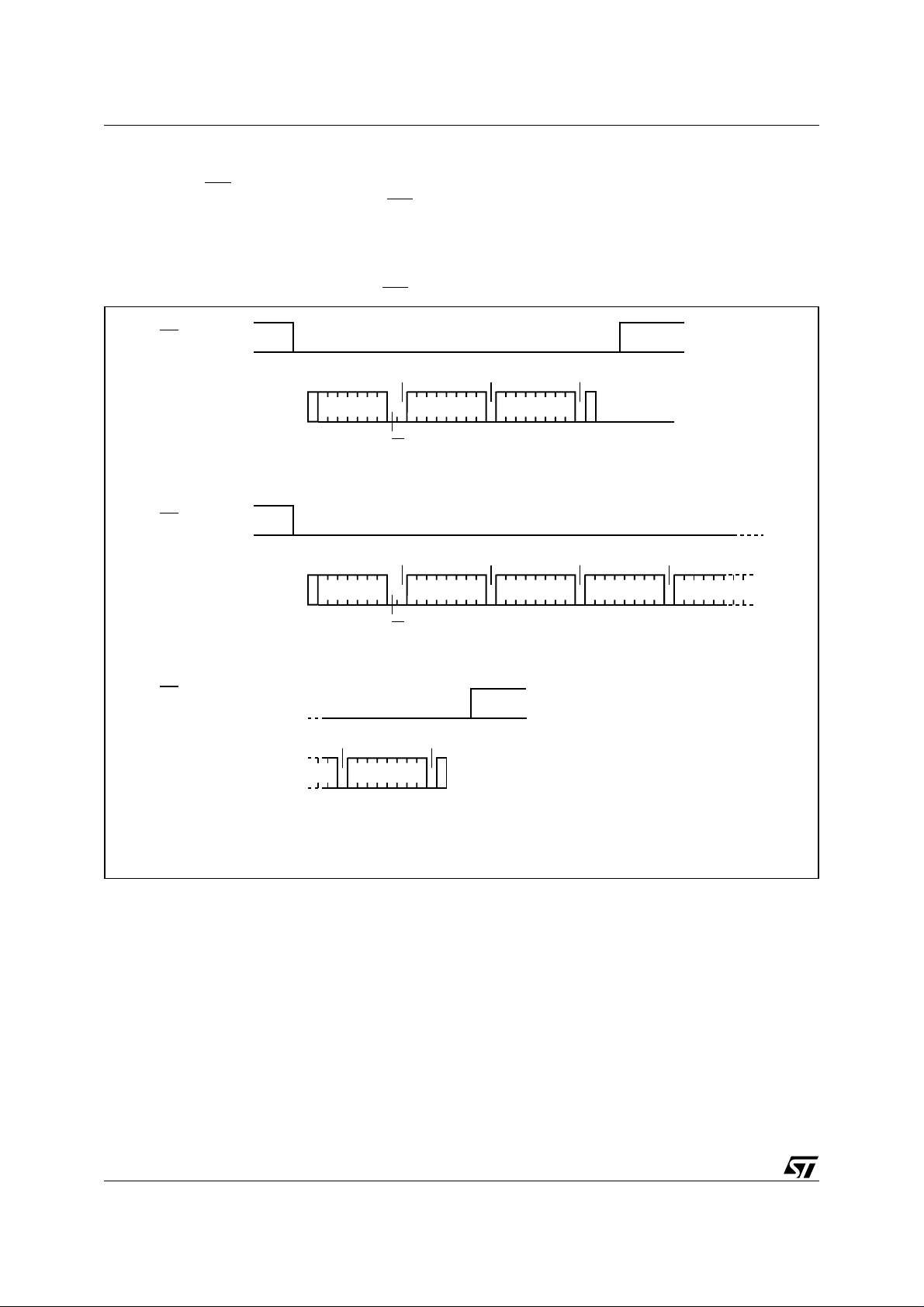
Figure 6. Write Mode Sequences, to Addresses in the Top Half, with WC=1 (data write inhibited)
WC
ACK ACK NO ACK
Byte Write DEV SEL BYTE ADDR DATA IN
R/W
START
WC
ACK ACK NO ACK NO ACK
Page Write DEV SEL BYTE ADDR
R/W
START
WC (cont'd)
NO ACK NO ACK
Page Write
(cont'd)
DATA IN N
STOP
STOP
DATA IN 1 DATA IN 2
DATA IN 3
AI02803C
Write Operations
Following a Start condition the bus master sends
a Device Select Code with the RW
bit reset to 0.
The device acknowledges this, as shown in
Figure 7, and waits for an address byte. The device responds to the address byte with an acknowledge bit, and then waits for the data byte.
When the bus master generates a Stop condition
immediately after the Ack bit (in the “10
th
bit” time
slot), either at the end of a Byte Write or a Page
Write, the internal memory Write cycle is t riggered.
A Stop condition at any other time slot does not
trigger the internal Write cycle.
During the internal Write cycle, Serial Data (SDA)
and Serial Clock (SCL) are ignored, and the device does not respond to any requests.
Byte Write
After the Device Select code and the address byte,
the bus master sends one data byte. If the ad-
dressed location is Write-protected, by Write Control (WC
) being driven High (during the period from
the Start condition until the end of the address
byte), the device replies to the data byte with
NoAck, as shown in Figure 6, and the location is
not modified. If, instead, the addressed location is
not Write-protected, the device replies with Ack.
The bus master terminates the transfer by generating a Stop condition, as shown in Figure 7.
Page Write
The Page Write mode allows up to 16 bytes to be
written in a single Write cycle, provided that they
are all located in the same page in the memory:
that is, the most significant memory address bits
are the same. If more bytes are sent than will fit up
to the end of the page, a condition known as ‘rollover’ occurs. This should be avoided, as data
starts to become overwritten in an implementation
dependent way.
9/21
Page 10
M34F04
The bus master sends from 1 to 16 bytes of data,
each of which is acknowledged by the device if
Write Control (WC
tion is Write-protected, by Writ e Control (WC
) is Low. If the addressed loca-
) being driven High (during the period from the Start
condition until the end of the address byte), the device replies to the data bytes with NoAck, as
Figure 7. Write Mode Sequences with WC
WC
BYTE WRITE DEV SEL BYTE ADDR
START
WC
PAGE WRITE DEV SEL BYTE ADDR
=0 (data write enabled)
ACK
R/W
ACK ACK ACK ACK
shown in Figure 6, and the locations are not modified. After each byte is transferred, the internal
byte address counter (the 4 least significant address bits only) is incremented. The transfer is terminated by the bus master generating a Stop
condition.
ACK ACK
DATA IN
STOP
DATA IN 1 DATA IN 2
DATA IN 3
WC (cont'd)
PAGE WRITE
(cont'd)
R/W
START
ACKACK
DATA IN N
STOP
AI02804B
10/21
Page 11
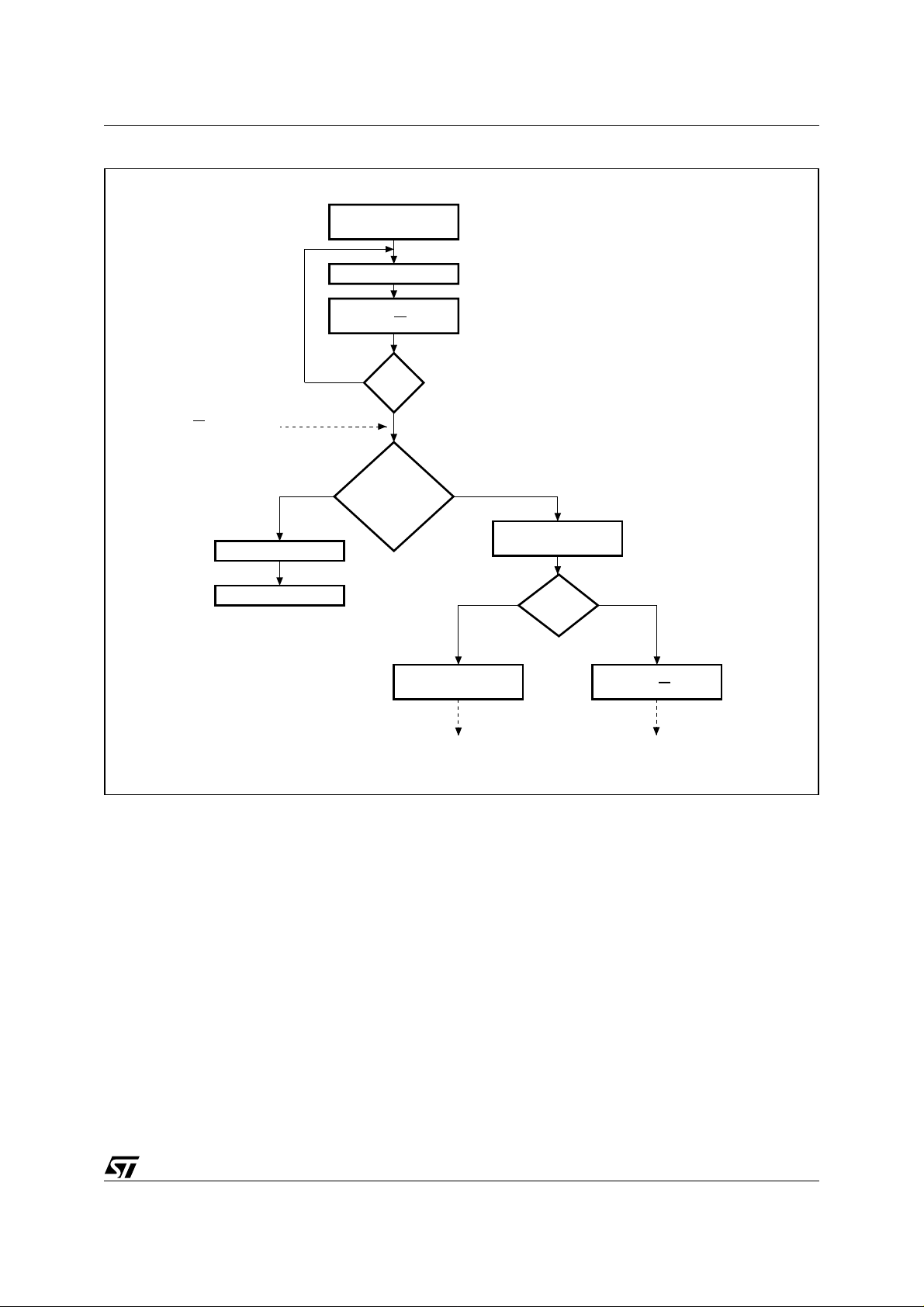
Figure 8. Write Cycle Polling Flowchart using ACK
WRITE Cycle
in Progress
START Condition
DEVICE SELECT
with RW = 0
ACK
NO
Returned
M34F04
First byte of instruction
with RW = 0 already
decoded by the device
ReSTART
STOP
YES
Next
Operation is
Addressing the
Memory
DATA for the
WRITE Operation
Continue the
WRITE Operation
Minimizing System Delays by Polling On ACK
During the internal Write cycle, the device disconnects itself from the bus, and writes a copy of the
data from its internal latches to the memory cells.
The maximum Write time (t
) is shown in Table 9,
w
but the typical time is shorter. To make use of this,
a polling sequence can be used by the bus master.
The sequence, as shown in Figure 8, is:
– Initial condition: a Write cycle is in progress.
YESNO
Send Address
and Receive ACK
START
Condition
YESNO
DEVICE SELECT
with RW = 1
Continue the
Random READ Operation
AI01847C
– Step 1: the bus master issues a Start condition
followed by a Device Select Code (the first byte
of the new instruction).
– Step 2: if the device is busy with the internal
Write cycle, no Ack will be returned and the bus
master goes back to Step 1. If the device has
terminated the internal Write cycle, it responds
with an Ack, indicating that the device is ready
to receive the second part of the instruct ion (the
first byte of this instruction having been sent
during Step 1).
11/21
Page 12

M34F04
Figure 9. Read Mode Sequences
CURRENT ADDRESS READ
RANDOM ADDRESS READ
SEQUENTIAL
CURRENT
READ
SEQUENTIAL
RANDOM
READ
ACK
DEV SEL DATA OUT
R/W
START
ACK
DEV SEL * BYTE ADDR
R/W
START
ACK ACK
DEV SEL DATA OUT 1
R/W
START
ACK ACK
DEV SEL * BYTE ADDR
NO ACK
STOP
ACK ACK
DEV SEL * DATA OUT
START
DEV SEL * DATA OUT 1
NO ACK
R/W
ACK NO ACK
DATA OUT N
ACK ACK
STOP
STOP
R/W
START
ACK NO ACK
DATA OUT N
STOP
Note: 1. The seven most significant bits of the Device Select Code of a Random Read (in the 1st and 3rd bytes) must be identical.
Read Operations
Read operations are performed independently of
the state of the Write Control (WC
) signal.
Random Address Read
A dummy Write is performed to load the address
into the address counter (as shown in Figure 9) but
without sending a Stop condition. Then, the bus
master sends another Start condition, and repeats
the Device Select Code, with the RW
bit set to 1.
The device acknowledges this, and outputs the
contents of the addressed byte. The bus master
START
must not acknowledge the byte, and terminates
the transfer with a Stop condition.
Current Address Read
The device has an internal address counter which
is incremented each time a byte is read. For the
Current Address Read operation, following a St art
condition, the bus master only sends a Device Select Code with the RW
knowledges this, and outputs the byte addressed
by the internal address counter. The counter is
then incremented. The bus master te rminates the
R/W
AI01942
bit set to 1. The device ac-
12/21
Page 13

M34F04
transfer with a Stop condition, as shown in
Figure 9, without acknowledging the byte.
Sequential Read
This operation can be used after a Current Address Read or a Random Address Read. The bus
master does acknowledge the data byte output,
and sends additional clock pulses so that the device continues to output the next byte in sequence.
To terminate the stream of by tes, the bus master
must not acknowledge the last byte, and must
generate a Stop condition, as shown in Figure 9.
The output data comes from consecutive addresses, with the internal address counter automatica lly
incremented after each byte output. After the last
memory address, the address counter ‘rolls-over’,
and the device continues to output data from
memory address 00h.
Acknowledge in Read Mode
For all Read commands, the device waits, after
each byte read, for an acknowledgme nt during the
th
bit time. If the bus master does not drive Serial
9
Data (SDA) Low during this time, the device terminates the data transfer and switches to its Standby mode.
INITIAL DELIVERY STATE
The device is delivered with all bits in the memory
array set to 1 (each Byte contains FFh).
13/21
Page 14

M34F04
MAXIMUM RATING
Stressing the device above the rating listed in the
Absolute Maximum Ratings" table may cause permanent damage to the device. These are stress
ratings only and operation of the device at these or
any other conditions above those indicated in the
plied. Exposure to Absolute Maximum Rating conditions for extended periods may affect device
reliability. Refer also to the STMicroelectronics
SURE Program and other relevant quality documents.
Operating sections of this specification is not im-
Table 4. Absolute Maximum Ratings
Symbol Parameter Min. Max. Unit
T
A
T
STG
V
IO
V
CC
V
ESD
Note: 1. AEC-Q 100-002 (compliant with JEDEC Std JESD 22-A114A, C1=100pF, R1=1500Ω, R2=500Ω)
Ambient Operating Temperature –40 125 °C
Storage Temperature –65 150 °C
Input or Output range –0.50 6.5 V
Supply Voltage –0.50 6.5 V
Electrostatic Discharge Voltage (Human Body model)
(1)
–4000 4000 V
14/21
Page 15
DC AND AC PARAMETERS
M34F04
This section summarizes the operating an d measurement conditions, and the DC and AC characteristics of the device. The parameters in the DC
and AC Characteristic tables that follow are derived from tests performed under the Measure-
ment Conditions summarized in the relevant
tables. Designers should check that the operating
conditions in their circuit match the measurement
conditions when relying on the quoted parameters.
Table 5. Operating Conditions
Symbol Parameter Min. Max. Unit
V
CC
T
A
Supply Voltage 2.5 5.5 V
Ambient Operating Temperature –40 85 °C
Table 6. AC Measurement Conditions
Symbol Parameter Min. Max. Unit
C
L
Load Capacitance 100 pF
Input Rise and Fall Times 50 ns
to 0.8V
Input Levels
Input and Output Timing Reference Lev els
0.2V
0.3V
CC
to 0.7V
CC
CC
CC
Figure 10. AC Measurement I/O Waveform
V
V
Table 7. Input Parameters
Symbol
C
IN
C
IN
Z
WCL
Z
WCH
t
NS
Note: 1. TA = 25 °C, f = 400 kHz
2. Sample d only, not 100% tested.
Input Capacitance (SDA) 8 pF
Input Capacitance (other pins) 6 pF
WC Input Impedance
WC Input Impedance
Pulse width ignored
(Input Filter on SCL and SDA)
Parameter
Input Levels
0.8V
CC
0.2V
CC
1,2
Input and Output
Timing Reference Levels
0.7V
CC
0.3V
CC
AI00825B
Test Condition Min. Max. Unit
V
IN
V
IN
< 0.3V
> 0.7V
CC
CC
570kΩ
500 kΩ
Single glitch 100 ns
15/21
Page 16
M34F04
Table 8. DC Characteristics
Symbol Parameter
Input Leakage Current
I
LI
(SCL, SDA)
I
I
I
CC1
V
V
V
Output Leakage Current
LO
Supply Current
CC
Stand-by Supply Current
Input Low Voltage
IL
(E2, E1, SCL, SDA)
Input High Voltage
IH
(E2, E1, SCL, SDA, WC
Output Low Voltage
OL
)
(in addition to those in Table 5.)
V
=2.5V, fc=400kHz (rise/fall time < 30ns)
CC
Table 9. AC Characteristics
Test conditions specified in Table 6. and Table 5.
Symbol Alt. Parameter Min. Max. Unit
f
C
t
CHCL
t
CLCH
(2)
t
DL1DL2
t
DXCX
t
CLDX
t
CLQX
(3)
t
CLQV
(1)
t
CHDX
t
DLCL
t
CHDH
t
DHDL
t
W
Note: 1. For a reSTART condition, or following a Write cycle.
2. Sample d only, not 100% tested.
3. To avoid spurious START and STOP conditions, a minimum delay is placed between SCL=1 and the falling or rising edge of SDA.
f
SCL
t
HIGH
t
LOW
t
F
t
SU:DAT
t
HD:DAT
t
DH
t
AA
t
SU:STA
t
HD:STA
t
SU:STO
t
BUF
t
WR
Clock Frequency 400 kHz
Clock Pulse Width High 600 ns
Clock Pulse Width Low 1300 ns
SDA Fall Time 20 300 ns
Data In Set Up Time 100 ns
Data In Hold Time 0 ns
Data Out Hold Time 200 ns
Clock Low to Next Data Valid (Access Time) 200 900 ns
Start Condition Set Up Time 600 ns
Start Condition Hold Time 600 ns
Stop Condition Set Up Time 600 ns
Time between Stop Condition and Next Start Condition 1300 ns
Write Time 5 ms
Test Condition
V
= VSS or V
IN
V
= VSS or V
OUT
V
= VSS or VCC, V
IN
I
= 2.1 mA, VCC = 2.5 V
OL
CC,
CC
SDA in Hi-Z
= 2.5 V
CC
Min. Max. Unit
± 2 µA
± 2 µA
1mA
0.5 µA
CC
0.3V
VCC+1
CC
–0.3
0.7V
0.4 V
V
V
16/21
Page 17
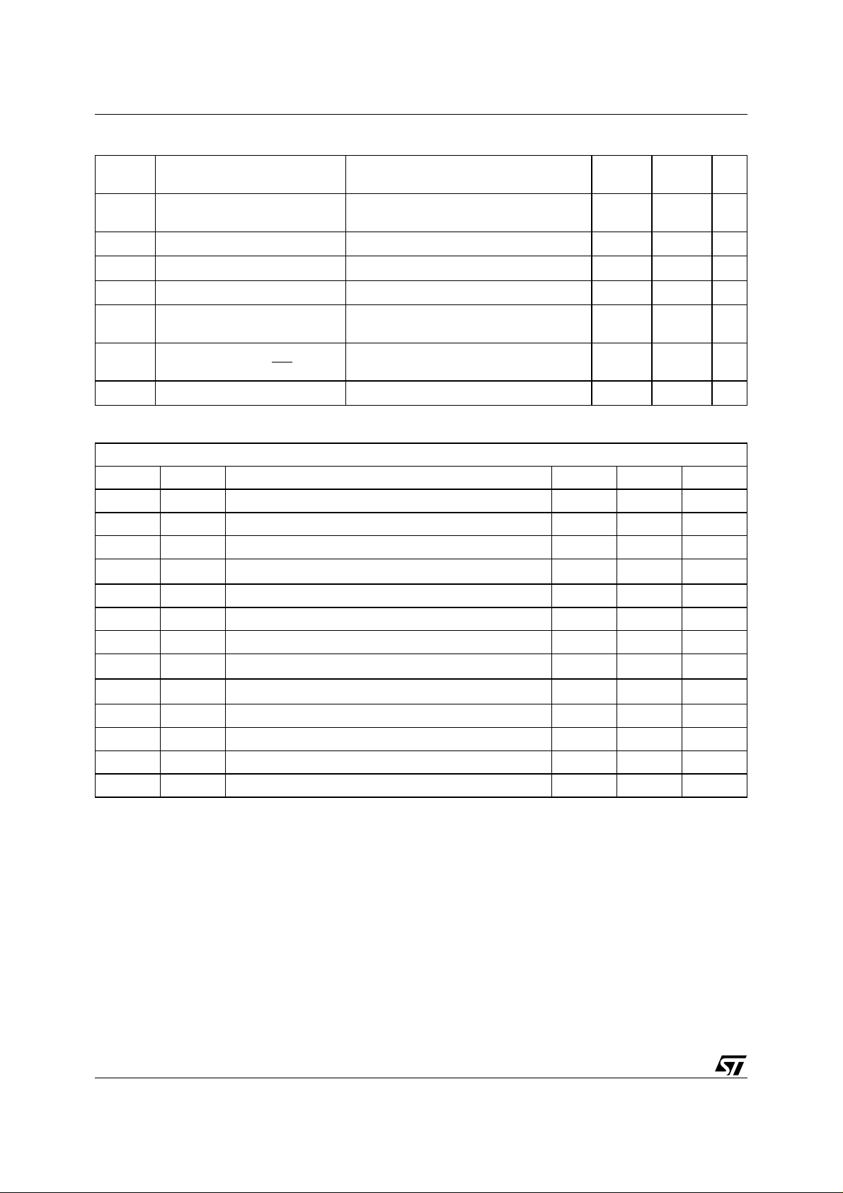
Figure 11. AC Waveforms
M34F04
SCL
SDA In
SCL
SDA In
SCL
tCHCL
tDLCL
tCHDX
START
Condition
tCHDH
STOP
Condition
tCLQV tCLQX
SDA
Input
tCLCH
SDA
Change
tW
Write Cycle
tDXCXtCLDX
tCHDH tDHDL
tCHDX
START
Condition
STOP
Condition
START
Condition
SDA Out
Data Valid
AI00795C
17/21
Page 18
M34F04
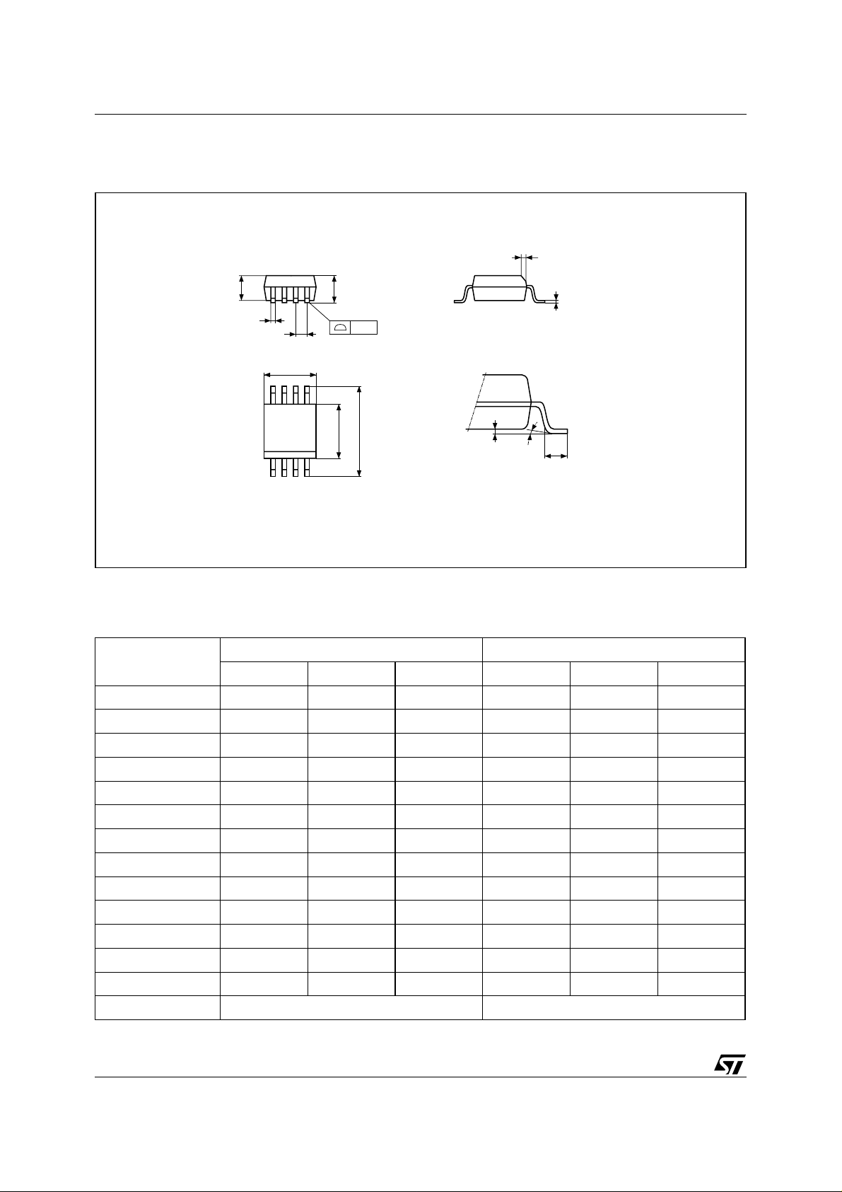
PACKAGE MECHANICAL
Figure 12. SO8 narrow – 8 lead Plastic Small Outline, 150 mils body width, Package Outline
h x 45˚
A2
B
e
D
8
1
Note: Drawing is not to scale.
A
ddd
E
H
C
LA1 α
Table 10. SO8 narrow – 8 lead Plastic Small Outline, 150 mils body width,
Package Mechanical Data
Symbol
Typ Min Max Typ Min Max
A 1.35 1.75 0.053 0.069
A1 0.10 0.25 0.004 0.010
A2 1.10 1.65 0.043 0.065
B 0.33 0.51 0.013 0.020
C 0.19 0.25 0.007 0.010
D 4.80 5.00 0.189 0.197
ddd 0.10 0.004
E 3.80 4.00 0.150 0.157
e 1.27 – – 0.050 – –
H 5.80 6.20 0.228 0.244
h 0.25 0.50 0.010 0.020
L 0.40 0.90 0.016 0.035
α 0° 8° 0° 8°
N (number of pins) 8 8
millimeters inches
SO-A
18/21
Page 19

PART NUMBERING
Table 11. Ordering Information Scheme
Example: M34F04 – W MN 6 T P
Device T ype
2
M34 = I
Device Function
04 = 4 Kbit (512 x 8)
Operating Voltage
W = V
Package
MN = SO8 (150 mil width)
Temperature Range
6 = –40 to 85 °C
Option
T = Tape & Reel Packing
C serial access EEPROM (ASSP)
= 2.5 to 5.5V (400kHz)
CC
M34F04
Plating Technology
blank = Standard SnPb plating
P or G = ECOPACK® (RoHs compliant)
(2)
For a list of available options (speed, package,
etc.) or for further information on any aspect of this
device, please contact your nearest ST Sales Office.
The category of Second-Level Interconnect is
marked on the package and on the inner box label,
in compliance with JEDEC Standard JESD97. The
maximum ratings related to soldering conditions
are also marked on the inner box label.
19/21
Page 20

M34F04
REVISION HISTORY
Table 12. Document Revision History
Date Version Description of Revision
23-Jan-2004 1.0 Document written
Document status promoted from Preliminary data to full Datasheet.
SO8 package specifications updated (see Table 10. and Figure 12.). SO8 package is
24-Jan-2006 2
compliant with ST ECOPACK® specifications. “Power On Reset” paragraph removed from
below SUMMARY DESCRIPTION. Supply voltage (V
DESCRIPTION section.
Table 4., Absolute Maximum Ratings updated.
) paragraph added to SIGNAL
CC
20/21
Page 21

M34F04
Information furnished is believe d to be accura te and re liable. Howev er, STMi croelec tronics assumes n o resp onsibil ity for t he consequences
of use of such information nor f or any infringement of pa tents or other rights of third parties which may re sult from its use. N o license is granted
by implication or otherwise und er an y pa ten t or patent rights of STMicroelectr on ics . Sp ec ific ations mentioned in this publication are subject
to change without notice. This publication supersedes and replaces all information previously supplied. STMicroelectronics products are not
authorized for use as critical components in life support devices or systems without express written approval of STMicroelectronics.
The ST logo is a registered trademark of STMicroelectronics.
All other names are the property of their respective owners
© 2006 STMicroelectronics - All rights reserved
Australia - Belgium - Brazil - Canada - China - Czech Republic - Finland - France - Germany - Hong Kong - India - Israel - Italy - Japan -
Malaysia - Malta - Morocco - Singapore - Spain - Sweden - Switzerland - United Kingdom - United States of America
STMicroelectronics group of companies
www.st.com
21/21
 Loading...