

2 Kbit serial presence detect (SPD) EEPROM
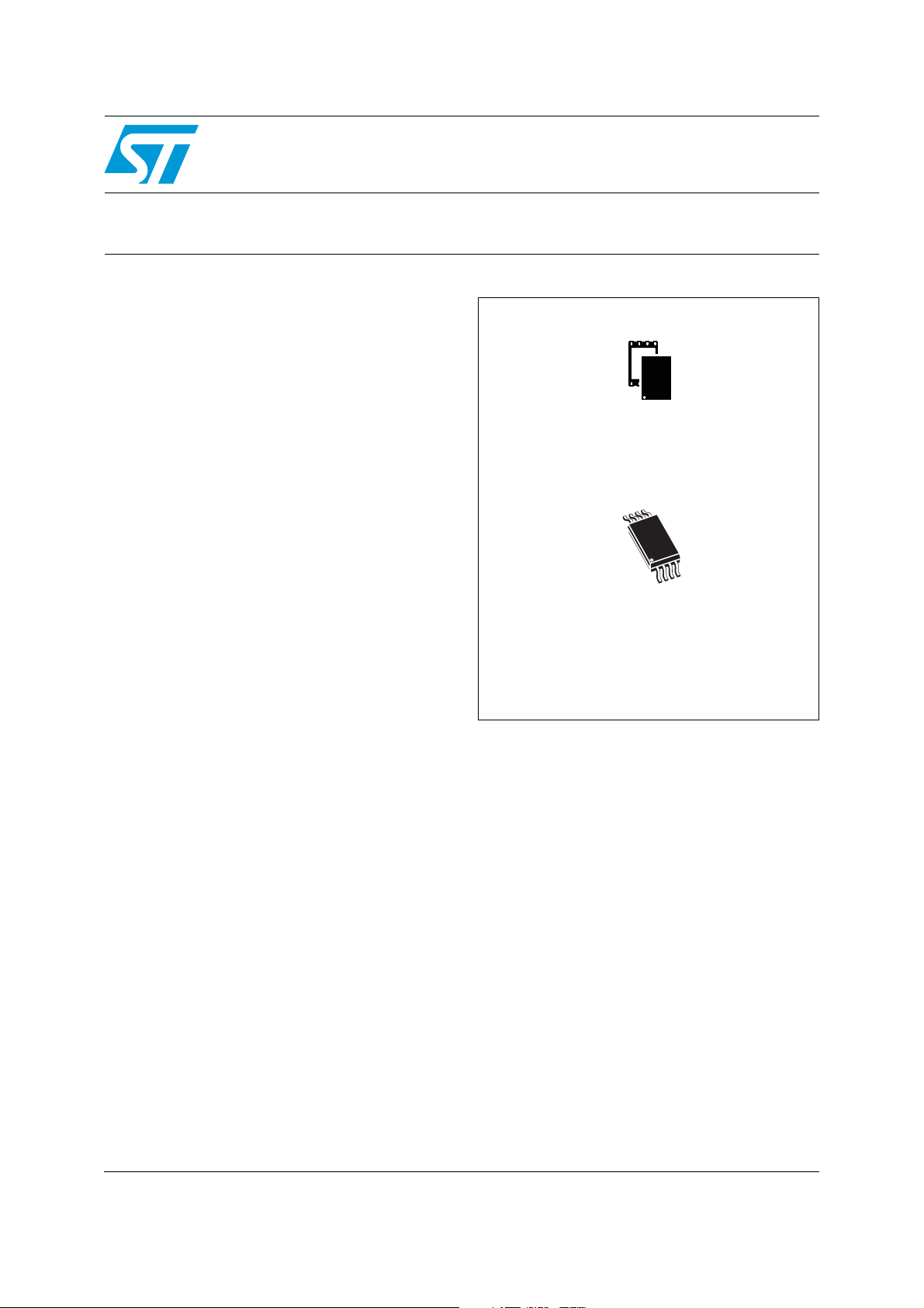
TSSOP8 (DW)
4.4 × 3 mm
UFDFPN8 (MB or MC)
2 x 3 mm
for double data rate (DDR1 and DDR2) DRAM modules
Features
■ 2 Kbit EEPROM for DDR1 and DDR2 serial
presence detect
■ Backward compatible with the M34C02
■ Permanent and reversible software data
protection for lower 128 bytes
■ 100 kHz and 400 kHz I
■ Single supply voltage:
– 1.7 V to 5.5 V
■ Byte and Page Write (up to 16 bytes)
■ Self-timed write cycle
■ Noise filtering
– Schmitt trigger on bus inputs
– Noise filter on bus inputs
■ Enhanced ESD/latch-up protection
■ More than 1 million erase/write cycles
■ More than 40 years’ data retention
■ ECOPACK
■ Packages:
– ECOPACK2
®
(RoHS compliant) packages
®
Halogen-free)
2
C bus serial interface
(RoHS-compliant and
M34E02
M34E02-F
May 2011 Doc ID 10367 Rev 11 1/34
www.st.com
1

Contents M34E02, M34E02-F
Contents
1 Description . . . . . . . . . . . . . . . . . . . . . . . . . . . . . . . . . . . . . . . . . . . . . . . . . 6
2 Signal description . . . . . . . . . . . . . . . . . . . . . . . . . . . . . . . . . . . . . . . . . . . 8
2.1 Serial Clock (SCL) . . . . . . . . . . . . . . . . . . . . . . . . . . . . . . . . . . . . . . . . . . . 8
2.2 Serial Data (SDA) . . . . . . . . . . . . . . . . . . . . . . . . . . . . . . . . . . . . . . . . . . . . 8
2.3 Chip Enable (E0, E1, E2) . . . . . . . . . . . . . . . . . . . . . . . . . . . . . . . . . . . . . . 8
2.4 Write Control (WC
2.5 Supply voltage (V
2.5.1 Operating supply voltage V
2.5.2 Power-up conditions . . . . . . . . . . . . . . . . . . . . . . . . . . . . . . . . . . . . . . . . 9
2.5.3 Device reset . . . . . . . . . . . . . . . . . . . . . . . . . . . . . . . . . . . . . . . . . . . . . . . 9
2.5.4 Power-down conditions . . . . . . . . . . . . . . . . . . . . . . . . . . . . . . . . . . . . . . 9
) . . . . . . . . . . . . . . . . . . . . . . . . . . . . . . . . . . . . . . . . . . . 8
) . . . . . . . . . . . . . . . . . . . . . . . . . . . . . . . . . . . . . . . . . 9
CC
CC . . . . . . . . . . . . . . . . . . . . . . . . . . . . . . . . . . . . . . . . . . 9
3 Device operation . . . . . . . . . . . . . . . . . . . . . . . . . . . . . . . . . . . . . . . . . . . 11
3.1 Start condition . . . . . . . . . . . . . . . . . . . . . . . . . . . . . . . . . . . . . . . . . . . . . 11
3.2 Stop condition . . . . . . . . . . . . . . . . . . . . . . . . . . . . . . . . . . . . . . . . . . . . . 11
3.3 Acknowledge bit (ACK) . . . . . . . . . . . . . . . . . . . . . . . . . . . . . . . . . . . . . . . 11
3.4 Data input . . . . . . . . . . . . . . . . . . . . . . . . . . . . . . . . . . . . . . . . . . . . . . . . . 11
3.5 Memory addressing . . . . . . . . . . . . . . . . . . . . . . . . . . . . . . . . . . . . . . . . . 12
3.6 Setting the write-protection . . . . . . . . . . . . . . . . . . . . . . . . . . . . . . . . . . . 13
3.6.1 SWP and CWP . . . . . . . . . . . . . . . . . . . . . . . . . . . . . . . . . . . . . . . . . . . 13
3.6.2 PSWP . . . . . . . . . . . . . . . . . . . . . . . . . . . . . . . . . . . . . . . . . . . . . . . . . . 13
3.7 Write operations . . . . . . . . . . . . . . . . . . . . . . . . . . . . . . . . . . . . . . . . . . . . 14
3.7.1 Byte Write . . . . . . . . . . . . . . . . . . . . . . . . . . . . . . . . . . . . . . . . . . . . . . . 14
3.7.2 Page Write . . . . . . . . . . . . . . . . . . . . . . . . . . . . . . . . . . . . . . . . . . . . . . . 14
3.7.3 Minimizing system delays by polling on ACK . . . . . . . . . . . . . . . . . . . . . 16
3.8 Read operations . . . . . . . . . . . . . . . . . . . . . . . . . . . . . . . . . . . . . . . . . . . . 16
3.8.1 Random Address Read . . . . . . . . . . . . . . . . . . . . . . . . . . . . . . . . . . . . . 16
3.8.2 Current Address Read . . . . . . . . . . . . . . . . . . . . . . . . . . . . . . . . . . . . . . 16
3.8.3 Sequential Read . . . . . . . . . . . . . . . . . . . . . . . . . . . . . . . . . . . . . . . . . . 16
3.8.4 Acknowledge in Read mode . . . . . . . . . . . . . . . . . . . . . . . . . . . . . . . . . 17
4 Initial delivery state . . . . . . . . . . . . . . . . . . . . . . . . . . . . . . . . . . . . . . . . . 18
2/34 Doc ID 10367 Rev 11

M34E02, M34E02-F Contents
5 Use within a DDR1/DDR2 DRAM module . . . . . . . . . . . . . . . . . . . . . . . 18
5.1 Programming the M34E02 and M34E02-F . . . . . . . . . . . . . . . . . . . . . . . . 18
5.1.1 Isolated DRAM module . . . . . . . . . . . . . . . . . . . . . . . . . . . . . . . . . . . . . 18
5.1.2 DRAM module inserted in the application motherboard . . . . . . . . . . . . 19
6 Maximum rating . . . . . . . . . . . . . . . . . . . . . . . . . . . . . . . . . . . . . . . . . . . . 22
7 DC and AC parameters . . . . . . . . . . . . . . . . . . . . . . . . . . . . . . . . . . . . . . 23
8 Package mechanical data . . . . . . . . . . . . . . . . . . . . . . . . . . . . . . . . . . . . 28
9 Part numbering . . . . . . . . . . . . . . . . . . . . . . . . . . . . . . . . . . . . . . . . . . . . 31
10 Revision history . . . . . . . . . . . . . . . . . . . . . . . . . . . . . . . . . . . . . . . . . . . 32
Doc ID 10367 Rev 11 3/34

List of tables M34E02, M34E02-F
List of tables
Table 1. Signal names . . . . . . . . . . . . . . . . . . . . . . . . . . . . . . . . . . . . . . . . . . . . . . . . . . . . . . . . . . . . 7
Table 2. Device select code . . . . . . . . . . . . . . . . . . . . . . . . . . . . . . . . . . . . . . . . . . . . . . . . . . . . . . . 10
Table 3. Operating modes . . . . . . . . . . . . . . . . . . . . . . . . . . . . . . . . . . . . . . . . . . . . . . . . . . . . . . . . 12
Table 4. DRAM DIMM connections . . . . . . . . . . . . . . . . . . . . . . . . . . . . . . . . . . . . . . . . . . . . . . . . . 18
Table 5. Acknowledge when writing data or defining the write-protection
(instructions with R/W bit = 0) . . . . . . . . . . . . . . . . . . . . . . . . . . . . . . . . . . . . . . . . . . . . . . . 19
Table 6. Acknowledge when reading the write protection (instructions with R/W bit = 1). . . . . . . . . 20
Table 7. Absolute maximum ratings . . . . . . . . . . . . . . . . . . . . . . . . . . . . . . . . . . . . . . . . . . . . . . . . . 22
Table 8. Operating conditions (for temperature range 1 devices) . . . . . . . . . . . . . . . . . . . . . . . . . . 23
Table 9. Operating conditions (for temperature range 6 devices) . . . . . . . . . . . . . . . . . . . . . . . . . . 23
Table 10. AC measurement conditions. . . . . . . . . . . . . . . . . . . . . . . . . . . . . . . . . . . . . . . . . . . . . . . . 23
Table 11. Input parameters. . . . . . . . . . . . . . . . . . . . . . . . . . . . . . . . . . . . . . . . . . . . . . . . . . . . . . . . . 24
Table 12. DC characteristics (for temperature range 1 devices) . . . . . . . . . . . . . . . . . . . . . . . . . . . . 24
Table 13. DC characteristics (for temperature range 6 devices) . . . . . . . . . . . . . . . . . . . . . . . . . . . . 25
Table 14. AC characteristics . . . . . . . . . . . . . . . . . . . . . . . . . . . . . . . . . . . . . . . . . . . . . . . . . . . . . . . . 26
Table 15. UFDFPN8 (MLP8) 8-lead ultra thin fine pitch dual flat package no lead
2 x 3 mm, data . . . . . . . . . . . . . . . . . . . . . . . . . . . . . . . . . . . . . . . . . . . . . . . . . . . . . . . . . . 29
Table 16. TSSOP8 – 8-lead thin shrink small outline, package mechanical data. . . . . . . . . . . . . . . . 30
Table 17. Ordering information scheme . . . . . . . . . . . . . . . . . . . . . . . . . . . . . . . . . . . . . . . . . . . . . . . 31
Table 18. Document revision history . . . . . . . . . . . . . . . . . . . . . . . . . . . . . . . . . . . . . . . . . . . . . . . . . 32
4/34 Doc ID 10367 Rev 11

M34E02, M34E02-F List of figures
List of figures
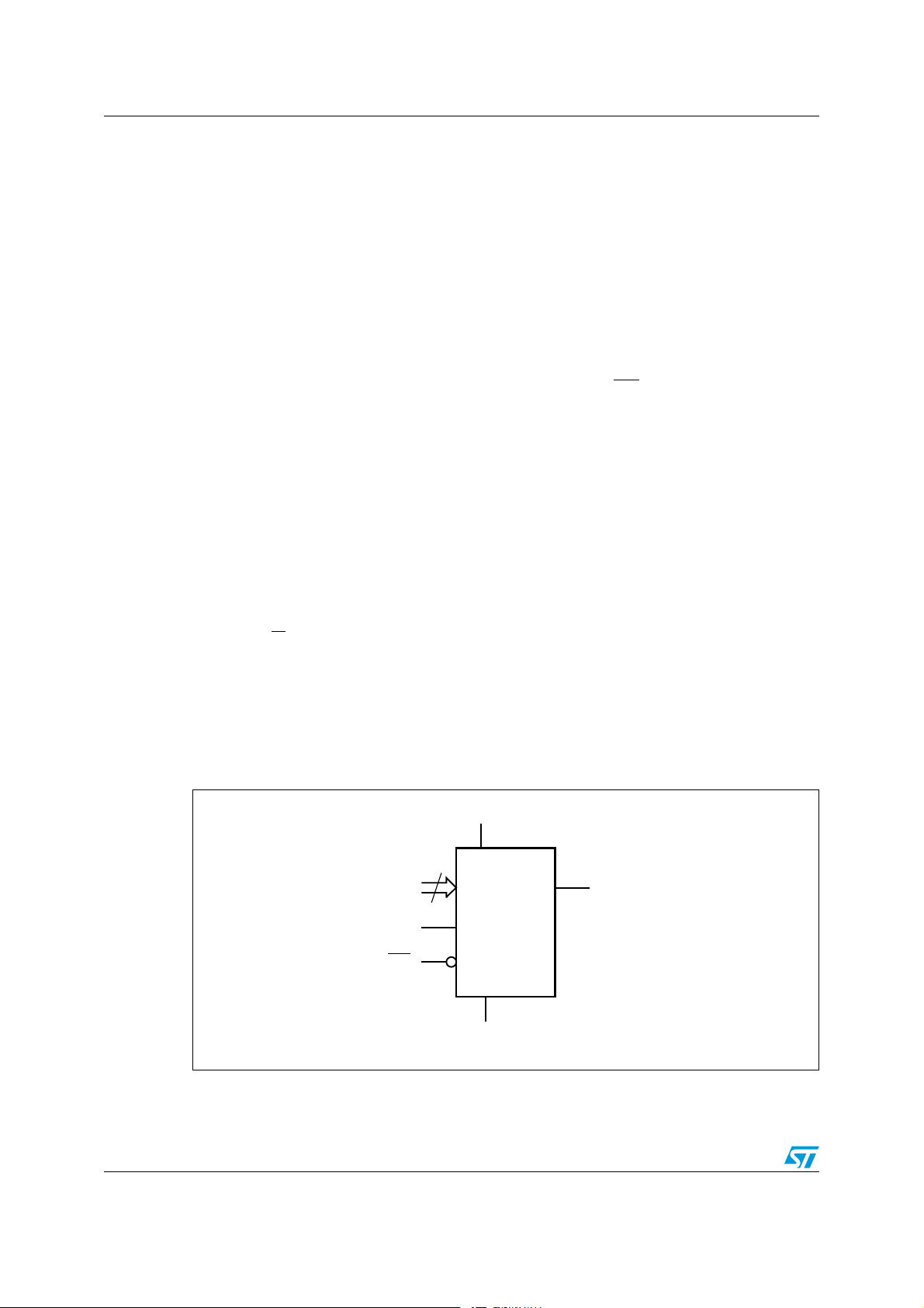
Figure 1. Logic diagram . . . . . . . . . . . . . . . . . . . . . . . . . . . . . . . . . . . . . . . . . . . . . . . . . . . . . . . . . . . . 6
Figure 2. TSSOP and MLP connections (top view) . . . . . . . . . . . . . . . . . . . . . . . . . . . . . . . . . . . . . . . 7
Figure 3. Device select code . . . . . . . . . . . . . . . . . . . . . . . . . . . . . . . . . . . . . . . . . . . . . . . . . . . . . . . . 8
Figure 4. Maximum R
Figure 5. I
Figure 6. Result of setting the write protection. . . . . . . . . . . . . . . . . . . . . . . . . . . . . . . . . . . . . . . . . . 12
Figure 7. Setting the write protection (WC
Figure 8. Write mode sequences in a non write-protected area . . . . . . . . . . . . . . . . . . . . . . . . . . . . 15
Figure 9. Write cycle polling flowchart using ACK . . . . . . . . . . . . . . . . . . . . . . . . . . . . . . . . . . . . . . . 15
Figure 10. Read mode sequences . . . . . . . . . . . . . . . . . . . . . . . . . . . . . . . . . . . . . . . . . . . . . . . . . . . . 17
Figure 11. Serial presence detect block diagram. . . . . . . . . . . . . . . . . . . . . . . . . . . . . . . . . . . . . . . . . 21
Figure 12. AC measurement I/O waveform . . . . . . . . . . . . . . . . . . . . . . . . . . . . . . . . . . . . . . . . . . . . . 23
Figure 13. AC waveforms . . . . . . . . . . . . . . . . . . . . . . . . . . . . . . . . . . . . . . . . . . . . . . . . . . . . . . . . . . 27
Figure 14. UFDFPN8 (MLP8) 8-lead ultra thin fine pitch dual flat package no lead
Figure 15. TSSOP8 – 8-lead thin shrink small outline, package outline . . . . . . . . . . . . . . . . . . . . . . . 30
2
C bus protocol . . . . . . . . . . . . . . . . . . . . . . . . . . . . . . . . . . . . . . . . . . . . . . . . . . . . . . . . . 10
2 x 3 mm, outline . . . . . . . . . . . . . . . . . . . . . . . . . . . . . . . . . . . . . . . . . . . . . . . . . . . . . . . . 29
value versus bus parasitic capacitance (C) for an I2C bus . . . . . . . . . . . . . . . 9
P
= 0) . . . . . . . . . . . . . . . . . . . . . . . . . . . . . . . . . . . . . . . . . 13
Doc ID 10367 Rev 11 5/34
Description M34E02, M34E02-F
1 Description
The M34E02 and M34E02-F are 2 Kbit serial EEPROM memories able to lock permanently
the data in its first half (from location 00h to 7Fh). This facility has been designed specifically
for use in DRAM DIMMs (dual interline memory modules) with serial presence detect (SPD).
All the information concerning the DDR1 or DDR2 configuration of the DRAM module (such
as its access speed, size and organization) can be kept write-protected in the first half of the
memory.
The first half of the memory area can be write-protected using two different software write
protection mechanisms. By sending the device a specific sequence, the first 128 bytes of
the memory become write protected: permanently or resettable. In addition, the devices
allow the entire memory area to be write protected, using the WC
tieing this input to V
These I
2
C-compatible electrically erasable programmable memory (EEPROM) devices are
CC
).
organized as 256 × 8 bits.
2
I
C uses a two wire serial interface, comprising a bi-directional data line and a clock line.
The devices carry a built-in 4-bit device type identifier code (1010) in accordance with the
2
I
C bus definition to access the memory area and a second device type identifier code
(0110) to define the protection. These codes are used together with the voltage level applied
on the three chip enable inputs (E2, E1, E0).
The devices behave as a slave device in the I
2
C protocol, with all memory operations
synchronized by the serial clock. Read and Write operations are initiated by a Start
condition, generated by the bus master. The Start condition is followed by a device select
code and RW
bit (as described in the Device select code table), terminated by an
acknowledge bit.
When writing data to the memory, the memory inserts an acknowledge bit during the 9
time, following the bus master’s 8-bit transmission. When data is read by the bus master, the
bus master acknowledges the receipt of the data byte in the same way. Data transfers are
terminated by a Stop condition after an Ack for WRITE, and after a NoAck for READ.
input (for example by
th
bit
Figure 1. Logic diagram
6
##
%% 3$!
-%
3#,
7#
6/34 Doc ID 10367 Rev 11
-%&
6
33
!)B
M34E02, M34E02-F Description
Figure 2. TSSOP and MLP connections (top view)
-%-%&
% 6
%
33
1. See the Package mechanical data section for package dimensions, and how to identify pin-1.
Table 1. Signal names
Signal names Description
E0, E1, E2 Chip Enable
SDA Serial Data
SCL Serial Clock
WC Write Control
V
CC
V
SS
Supply voltage
Ground
##
7#%
3#,
3$!6
!)B
Doc ID 10367 Rev 11 7/34

Signal description M34E02, M34E02-F
!IB
6
##
6
33
%
I
6
##
-%
-%&
6
33
%
I
-%
-%&
2 Signal description
2.1 Serial Clock (SCL)
This input signal is used to strobe all data in and out of the device. In applications where this
signal is used by slave devices to synchronize the bus to a slower clock, the bus master
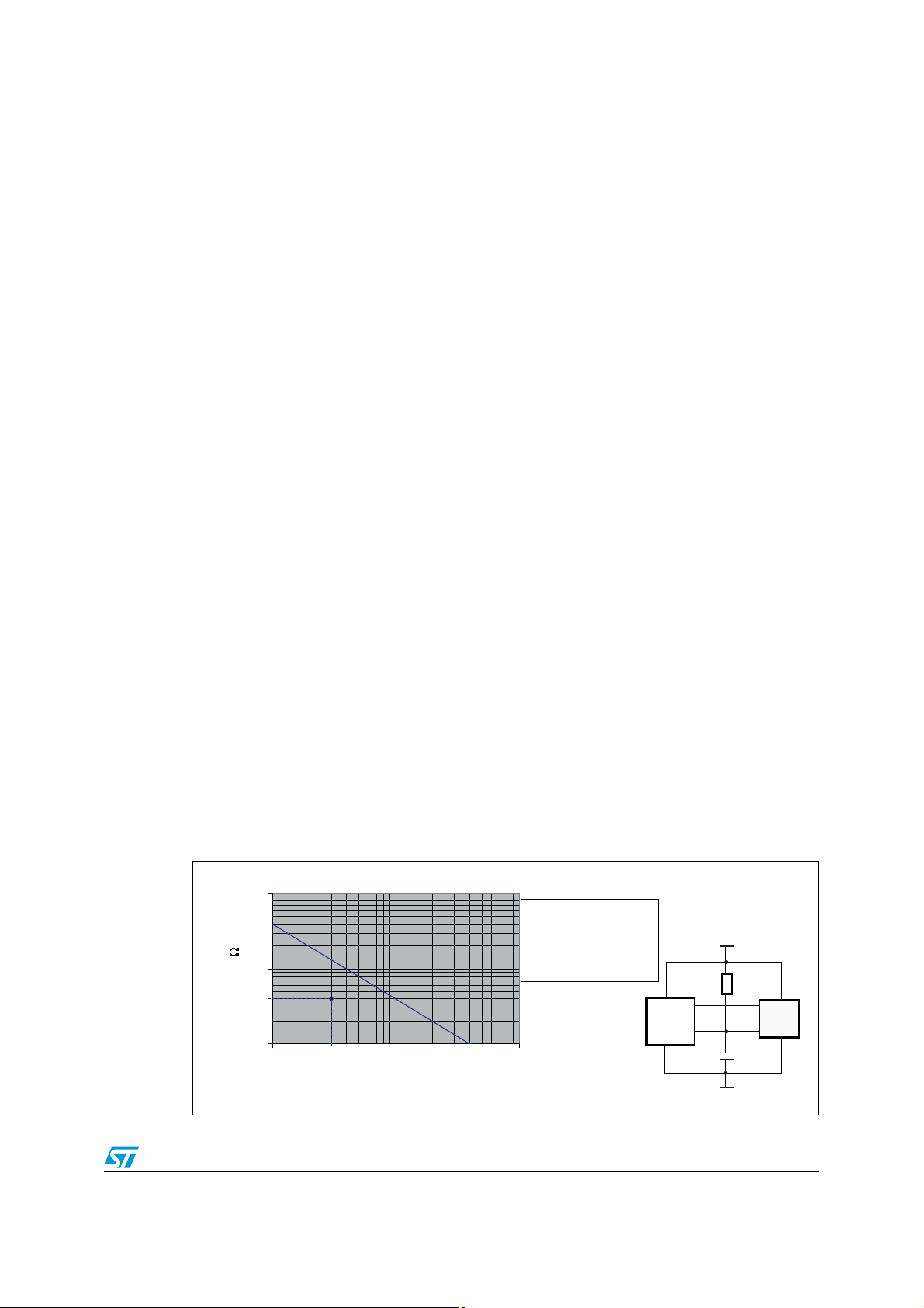
must have an open drain output, and a pull-up resistor can be connected from Serial Clock
(SCL) to V
most applications, though, this method of synchronization is not employed, and so the pullup resistor is not necessary, provided that the bus master has a push-pull (rather than open
drain) output.
2.2 Serial Data (SDA)
This bidirectional signal is used to transfer data in or out of the device. It is an open drain
output that may be wire-OR’ed with other open drain or open collector signals on the bus. A
pull up resistor must be connected from Serial Data (SDA) to V
the value of the pull-up resistor can be calculated).
. (Figure 4 indicates how the value of the pull-up resistor can be calculated). In
CC
. (Figure 4 indicates how
CC
2.3 Chip Enable (E0, E1, E2)
These input signals are used to set the value that is to be looked for on the three least
significant bits (b3, b2, b1) of the 7-bit device select code. In the end application, E0, E1 and
E2 must be directly (not through a pull-up or pull-down resistor) connected to V
establish the device select code. When these inputs are not connected, an internal pulldown circuitry makes (E0,E1,E2) = (0,0,0).
The E0 input is used to detect the V
Figure 3. Device select code
2.4 Write Control (WC)
This input signal is provided for protecting the contents of the whole memory from
inadvertent write operations. Write Control (WC
disable (when driven high) write instructions to the entire memory area or to the Protection
Register.
or VSS to
CC
voltage, when decoding an SWP or CWP instruction.
HV
) is used to enable (when driven low) or
When Write Control (WC
) is tied low or left unconnected, the write protection of the first half
of the memory is determined by the status of the Protection Register.
8/34 Doc ID 10367 Rev 11
M34E02, M34E02-F Signal description
1
10
100
10 100 1000
Bus line capacitor (pF)
Bus line pull-up resistor
(k
)
When t
LOW
= 1.3 µs (min value for
f
C
= 400 kHz), the R
bus
× C
bus
time constant m ust be below the
400 ns time constant line
represented on the left.
2.5 Supply voltage (VCC)
2.5.1 Operating supply voltage V
Prior to selecting the memory and issuing instructions to it, a valid and stable VCC voltage
within the specified [V
(min), VCC(max)] range must be applied (see Tab l e 8 ). In order to
CC
secure a stable DC supply voltage, it is recommended to decouple the V
suitable capacitor (usually of the order of 10 nF to 100 nF) close to the V
pins.
This voltage must remain stable and valid until the end of the transmission of the instruction
and, for a Write instruction, until the completion of the internal write cycle (t
2.5.2 Power-up conditions
The VCC voltage has to rise continuously from 0 V up to the minimum VCC operating voltage
defined in Ta bl e 8 and the rise time must not vary faster than 1 V/µs.
2.5.3 Device reset
In order to prevent inadvertent write operations during power-up, a power-on reset (POR)
circuit is included. At power-up, the device does not respond to any instruction until V
reaches the internal reset threshold voltage (this threshold is lower than the minimum V
operating voltage defined in Ta bl e 8 ).
When V
Power mode. However, the device must not be accessed until V
stable V
In a similar way, during power-down (continuous decrease in V
below the power-on reset threshold voltage, the device stops responding to any instruction
sent to it.
passes over the POR threshold, the device is reset and enters the Standby
CC
voltage within the specified [VCC(min), VCC(max)] range.
CC
CC
line with a
CC
CC/VSS
reaches a valid and
CC
), as soon as VCC drops
CC
).
W
package
CC
CC
2.5.4 Power-down conditions
During power-down (continuous decrease in VCC), the device must be in Standby Power
mode (mode reached after decoding a Stop condition, assuming that there is no internal
write cycle in progress).
Figure 4. Maximum R
Here R
× C
bus
4 kΩ
bus
30 pF
value versus bus parasitic capacitance (C) for an I2C bus
P
R
bus
× C
bus
= 120 ns
V
CC
R
SCL
SDA
bus
M24xxx
C
bus
ai14796b
= 400 ns
I²C bus
master
Doc ID 10367 Rev 11 9/34
Signal description M34E02, M34E02-F
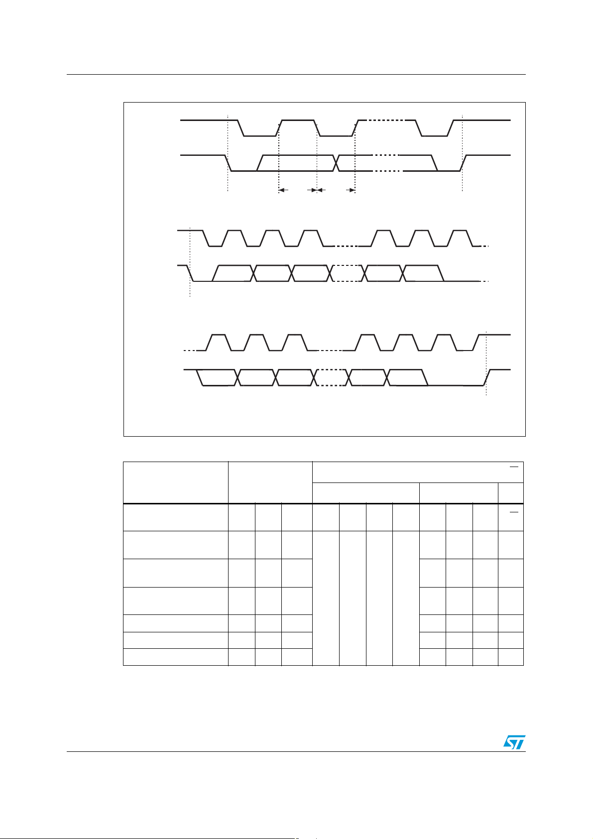
Figure 5. I2C bus protocol
SCL
SDA
Start
condition
SCL
SDA
Start
condition
SCL
SDA
Table 2. Device select code
1 23 7 89
MSB
1 23 7 89
MSB ACK
Chip Enable
signals
SDA
Input
SDA
Change
Stop
condition
ACK
Stop
condition
AI00792c
Device type identifier Chip Enable bits RW
(1)
b7
b6 b5 b4 b3 b2 b1 b0
Memory area select
code (two arrays)
(2)
Set write protection
(SWP)
Clear write protection
(CWP)
Permanently set write
protection (PSWP)
(2)
Read SWP V
Read CWP V
Read PSWP
1. The most significant bit, b7, is sent first.
2. E0, E1 and E2 are compared against the respective external pins on the memory device.
3. VHV is defined in Table 13.
(2)
E2 E1 E0 1 0 1 0 E2 E1 E0 RW
V
SSVSSVHV
V
SSVCCVHV
E2 E1 E0 E2 E1 E0 0
SSVSSVHV
SSVCCVHV
(3)
(3)
0110
(3)
(3)
E2 E1 E0 E2 E1 E0 1
10/34 Doc ID 10367 Rev 11
0010
0110
0011
0111

M34E02, M34E02-F Device operation
3 Device operation
The device supports the I2C protocol. This is summarized in Figure 5 Any device that sends
data on to the bus is defined to be a transmitter, and any device that reads the data to be a
receiver. The device that controls the data transfer is known as the bus master, and the
other as the slave device. A data transfer can only be initiated by the bus master, which will
also provide the serial clock for synchronization. The memory device is always a slave in all
communication.
3.1 Start condition
Start is identified by a falling edge of Serial Data (SDA) while Serial Clock (SCL) is stable in
the high state. A Start condition must precede any data transfer command. The device
continuously monitors (except during a Write cycle) Serial Data (SDA) and Serial Clock
(SCL) for a Start condition.
3.2 Stop condition
Stop is identified by a rising edge of Serial Data (SDA) while Serial Clock (SCL) is stable
and driven high. A Stop condition terminates communication between the device and the
bus master. A Read command that is followed by NoAck can be followed by a Stop condition
to force the device into the Standby mode. A Stop condition at the end of a Write command
triggers the internal EEPROM Write cycle.
3.3 Acknowledge bit (ACK)
The acknowledge bit is used to indicate a successful byte transfer. The bus transmitter,
whether it be bus master or slave device, releases Serial Data (SDA) after sending eight bits
of data. During the 9
acknowledge the receipt of the eight data bits.
th
clock pulse period, the receiver pulls Serial Data (SDA) low to
3.4 Data input
During data input, the device samples Serial Data (SDA) on the rising edge of Serial Clock
(SCL). For correct device operation, Serial Data (SDA) must be stable during the rising edge
of Serial Clock (SCL), and the Serial Data (SDA) signal must change only when Serial Clock
(SCL) is driven low.
Doc ID 10367 Rev 11 11/34
 Loading...