

查询M34C02供应商
M34C02
2 Kbit Serial I²C Bus EEPROM
For DIM M Serial P resence Detect
■ Two Wire I
2
C Serial Interface
Supports 400 kHz Protocol
■ Single Supply Voltage:
– 2.5V to 5.5V for M34C02-W
– 2.2V to 5.5V for M34C02-L
■ Software Data Protection for lower 128 bytes
■ BYTE and PAGE WRITE (up to 16 bytes)
■ RANDOM and SEQUENTIAL READ Modes
■ Self-Tim ed P ro gr a m ming Cycle
■ Automatic Address Incrementing
■ Enhanced ESD/Latch-Up Protection
■ 1 Million Erase/Write Cycles (minimum)
■ 40 Year Data Retention (minimum)
DESCRIPTION
The M34C02 is a 2 Kbit serial EEPROM memory
able to lock permanently the data in its first half
(from location 00h to 7Fh). This facility has been
designed specifically for use in DRAM DIMMs
(dual interline memory modules) with Serial
Presence Detect. All the information concerning
the DRAM module configuration (such as its
access speed, its size, its organization) can be
kept write protected in the first half of the memory.
This bottom half of the memory area can be writeprotected using a specially designed software
write protection mechanism. By sending the
device a specific sequence, the first 128 bytes of
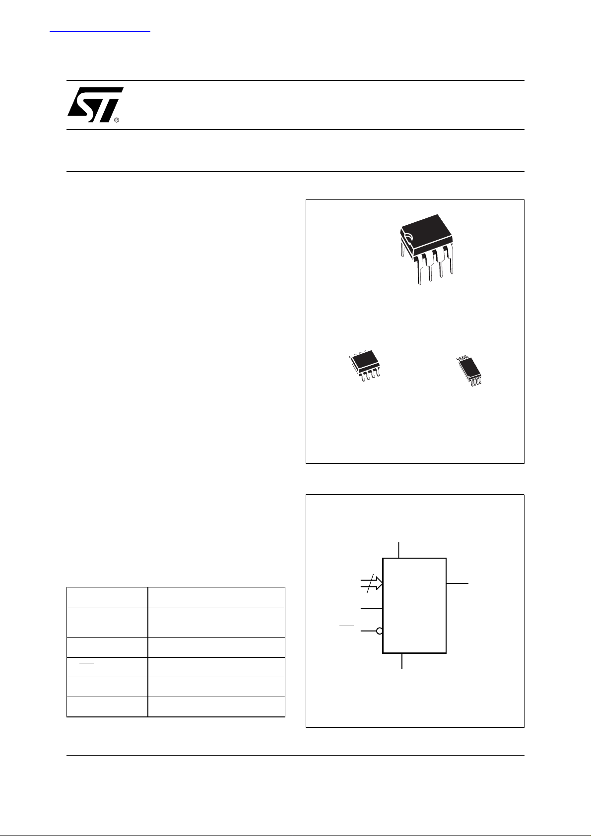
8
PSDIP8 (BN)
0.25 mm frame
8
1
SO8 (MN)
150 mil width
Figure 1. Logic Diagram
V
CC
1
8
1
TSSOP8 (DW)
169 mil width
Table 1. Signal Names
E0, E1, E2 Chip Enable Inputs
SDA Serial Data/Address Input/
Output
SCL Serial Clock
WC
V
CC
V
SS
Write Control
Supply Voltage
Ground
3
E0-E2 SDA
SCL
WC
M34C02
V
SS
AI01931
1/19December 1999
M34C02
Figure 2A. DIP Connections
M34C02
1
E0 V
2
3
E2
4
SS
8
7
6
5
AI01932
CC
WCE1
SCL
SDAV
the memory become permanently write protected.
Care must be taken w hen us i ng this s equence as
its effect cannot be reversed. In addition, the
device allows the entire m emory area to be write
protected, using the WC
tieing this input to V
input (for example by
).
CC
The M34C02 is a 2 Kbit electrically erasable programmable memory (EEPROM), organized as
256x8 bits, fabricated with STMicroelectronics’
High Endurance, Advanced, CMOS technology.
This guarantees an endurance typically well
above one millio n Erase/Wri te cycles, with a data
retention of 40 years. These memory devices
operate with a power supply down to 2.2 V for the
M34C02-L.
The M34C02 is available in Plastic Dual In-line,
Plastic Small Outline and Thin Shrink Small
Outline packages.
These memory devices are compatible with the
2
C memory standard. This is a two wire serial
I
Figure 2B. SO and TSSOP Connections
M34C02
1
E0 V
2
3
E2
SS
4
8
7
6
5
AI01933
CC
WCE1
SCL
SDAV
interface that uses a bi-directional data bus and
serial clock. The memory carries a built-in 4-bit
Device Type Identifier code (1010) in accordance
with the I
2
C bus definition to access the memory
area and a second Device Type Identifier Code
(0110) to access the Protection Regist er. These
codes are used together with three chip enable
inputs (E2, E1, E0) so that up to eight 2 Kbit
devices may be attached to the I²C bus and
selected individually.
The memory behaves as a slave device in the I
2
protocol, with all memory operations synchronized
by the serial clock. Read and Write operations are
initiated by a START condition, genera ted by the
bus master. The START condition is followed by a
Device Select Code and RW
bit (as described in
Table 3), terminated by an acknowledge bit.
When writing data to the memory, the memory
inserts an acknowledge bit during the 9
th
bit time,
following the bus master’s 8-bit transmission.
C
Table 2. Absolute Maximum Ratings
Symbol Parameter Value Unit
T
A
T
STG
T
LEAD
V
IO
V
CC
V
ESD Electrostatic Discharge Voltage (Human Body model)
Note: 1. Exc ept for the rat i ng “Operating Temperatu re Range”, s tr esses above those listed in the Table “Absolute Maximum Ratings” may
2/19
cause permanent damage to the device. These are stress ratings only, and operation of the device at these or any other conditions
above those indicated in the Operating se ct i ons of this specification is not im plied. Expo sure to Absolute Maximum Rating conditions for extended periods may affect device reliability. Refer also to the ST SURE Program and other relevant quality documents.
2. MIL -STD-883C, 3015.7 (100 pF, 1500 Ω)
Ambient Operating Temperature -40 to 85 °C
Storage Temperature -65 to 150 °C
Lead Temperature during Soldering
Input or Output range -0.6 to 6.5 V
Supply Voltage -0.3 to 6.5 V
1
PSDIP8: 10 sec
SO8: 40 sec
TSSOP8: 40 sec
2
260
215
215
4000 V
°C
M34C02
When data is read by the bus master, the bus
master acknowledges the receipt of the data byte
in the same way. Data transfers are terminated by
a STOP condition after an Ack for WRITE, and
after a NoAck for READ.
Power On Reset: V
Lock-Out Write Protect
CC
In order to prevent data corruption and inadvertent
write operations during power up, a Power On
Reset (POR) circuit is included. The internal reset
is held active until the V
voltage has reached
CC
the POR threshold value, and all operations are
disabled – the device will not respond to any
command. In the same way, when V
drops from
CC
the operating voltage, below the POR threshold
value, all operations are disabled an d the device
will not respond to any command. A stable and
valid V
must be applied before applying any
CC
logic signal.
SIGNAL DESCRIPTION
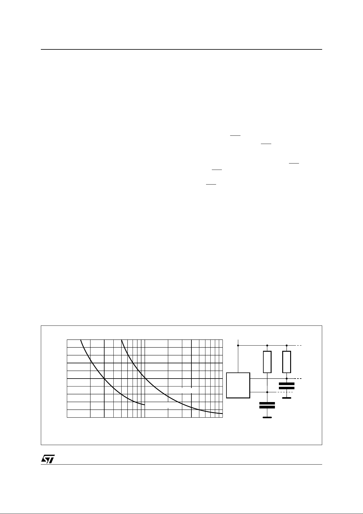
Serial Clock (SCL)
The SCL input pin is used to strobe all data in and
out of the memory. In applications where this line
is used by slaves to synchronize the bus to a
slower clock, the master must have an open drain
output, and a pull-up resistor must be c onnected
from the SCL line to V
. (Figure 3 indicates how
CC
the value of the pull-up resistor can be calculated).
In most applications, though, this method of
synchronization is not employed, and so the pullup resistor is not necessary, provided that the
master has a push-pull (rather than open drain)
output.
Serial Data (SDA)
The SDA pin is bi-directional, and is used to
transfer data in or out of the memory. It is an open
drain output that may be wire-OR’ed with other
open drain or open collector signals on the bus. A
pull up resistor must be connected f rom the SDA
bus to V
. (Figure 3 indicates how t he value of
CC
the pull-up resistor can be calculated).
Chip Enable (E2, E1, E0)
These chip enable inputs are used to set the value
that is to be looked for on the three least significant
bits (b3, b2, b1) of the 7-bit device select code.
These inputs may be driven dynamically or tied to
or VSS to establish the device select code.
V
CC
Write Control (WC
A hardware Write Control (WC
)
, pin 7) is provided
for protecting the contents of the whole memory
from erroneous erase/write cycles. The Write
Control signal is used to enable (WC
disable (WC
=VIH) write instructions to the entire
=VIL) or
memory area or to the Protection Register.
When WC
is tied to VSS or left unc onnected, the
write protection of the first half of the memory is
determined by the status of the Protection
Register.
DEVICE OPERATION
The memory device supports the I
2
C protocol.
This is summarized in Figure 4. Any device that
sends data on to the bus is defined to be a
transmitter, and any device that reads the data to
be a receiver. The device that controls the data
transfer is known as the master, and the other as
the slave. A data transfer can o nly be initiated by
the master, which will also provide the serial clock
for synchronization. The memory device is always
a slave device in all communication.
Figure 3. Maximum R
20
16
12
8
Maximum RP value (kΩ)
4
0
10 1000
Value versus Bus Capacitance (C
L
fc = 100kHz
fc = 400kHz
100
C
(pF)
BUS
) for an I2C Bus
BUS
MASTER
V
CC
R
SDA
SCL
R
C
BUS
L
C
BUS
AI01665
3/19
L
M34C02
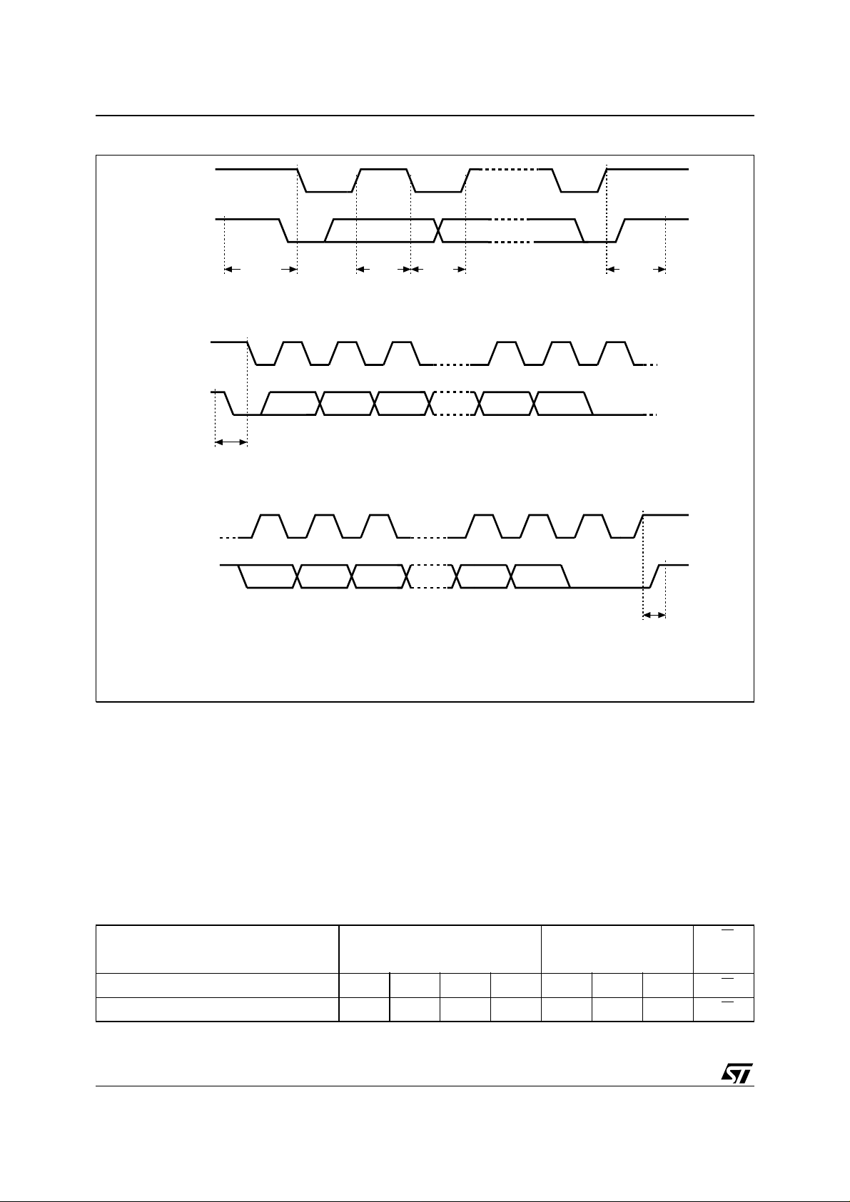
Figure 4. I
2
C Bus Protocol
SCL
SDA
SCL
SDA
SCL
SDA
START
CONDITION
START
CONDITION
SDA
INPUT
1 23 789
MSB
1 23 789
MSB ACK
SDA
CHANGE
CONDITION
ACK
STOP
STOP
CONDITION
AI00792
Start Condition
START is identified by a high t o low transition of
the SDA line while the clock, SCL, is stable in t he
high state. A START condition must precede any
data transfer command. The memory device
continuously monitors (except during a
programming cycle) the SDA and SCL lines for a
START condition, and will not respond unless one
is given.
Table 3. Device Select Code
1
Stop Condition
STOP is identified by a low to high transition of the
SDA line wh ile th e clock S CL is sta ble in the h igh
state. A STOP condition terminates
communication between the m emory device and
the bus master. A STOP condition at the end of a
Read command, provided th at it is followed by a
NoAck, forces the memory device into its st andby
state. A STOP condition at the end of a Write
Device Type Identifier Chip Enable RW
b7 b6 b5 b4 b3 b2 b1 b0
Memory Area Select Code (two arrays) 1 0 1 0 E2 E1 E0 RW
Protection Register Select Code 0 1 1 0 E2 E1 E0 RW
Note: 1. The most significant bit (b7) is sent first.
4/19

M34C02
Table 4. Operating Modes
Mode RW bit
Current Address Read 1 X 1 START, Device Select, RW
0X
Random Address Read
1 X reSTART, Device Select, RW
Sequential Read 1 X ≥ 1 Similar to Current or Random Address Read
WC
1
Bytes Initial Sequence
= ‘1’
1
START, Device Select, RW
= ‘0’, Address
= ‘1’
Byte Write 0
Page Write 0
Note: 1. X = V
IH
or V
.
IL
V
IL
V
IL
command triggers the internal EEPROM write
cycle.
Acknowledge Bit (ACK)
An acknowledge signal is used to indicate a
successful byte transfer. The bus transmitter,
whether it be master or slave, releases the SDA
bus after sending eight bits of data. During the 9
clock pulse period, the receiver pulls the SDA bus
low to acknowledge the receipt of the eight data
bits.
Data Input
During data input, the memory device samples the
SDA bus signal on the rising edge of the clock,
SCL. For correct device operation, the SDA signal
must be stable during the clock low-to-high
only
transition, and the data must change
when
the SCL line is low .
Memory Addressing
To start communication betwee n the bus master
and the slave memory, the master must initiate a
START condition. Following this, the master sends
the 8-bit byte, shown in Table 3, on the SDA bus
line (most significant bit first). This consists of the
7-bit Device Select Code, and the 1-bit Read/Write
Designator (RW). The Device Select Code is
further subdivided into: a 4-bit Device Type
Identifier, and a 3-bit Chip Enable “Address” (E2,
E1, E0 ) .
To address the memory array, the 4-bit Device
Type Identifier is 1010b. To address the Protection
Register, it is 0110b.
If all three chip enable inputs are connected, up to
eight memory devices can be connected on a
single I
2
C bus. Each one is given a unique 3-bit
code on its Chip Enable inputs. When t he Device
Select Code is received on the SDA bus, the
memory only responds if t he Chip Select Code is
the same as the pattern applied to its Chip Enable
pins.
th
The 8
bit is the read or write bit (RW). This bit is
set to ‘1’ for read and ‘0’ for write operations. If a
1 START, Device Select, RW = ‘0’
≤ 16 START, Device Select, RW = ‘0’
match occurs on the Device Select Code, the
corresponding memory gives an acknowledgment
on the SDA bus during the 9
th
bit time. If the
memory does not match the Device Select code, it
will deselect itself from the bus, and go into standby mode.
th
Write Operations
Following a START con dition the ma ster sends a
Device Select Code with the RW
bit set to ’0’, as
shown in Table 4. The memory acknowledges this,
and waits for an address byte. The memory
responds to the address byte with an acknowledge
bit, and then waits for the data byte.
Writing to the memory may be inhibited if the WC
input pin is taken high.
Byte Write
In the Byte Write mode, after the Device Select
Code and the address byte, the master sends one
data byte. If the addressed location is in a write
protected area, the memory replies with a NoA ck,
and the location is not modified. If, instead, the
addressed location is not in a write protected area,
the memory replies with an Ack. The master
terminates the transfer by generating a STOP
condition.
Page Write
The Page Write mode allows u p to 16 bytes to be
written in a single write cycle, provided that they
are all located in the same ’row’ in the memory:
that is the most significant memory add ress bits
(b7-b4) are the same. I f m ore byt es are sent than
will fit up to t he en d of t he row, a condition known
as ‘roll-over’ occurs. Data starts to become
overwritten (in a way not formally specified in this
data sheet).
The master sends from one up to 16 bytes of data,
each of which is acknow ledged by the memory if
the WC
pin is low. If the WC pin is high, the
contents of the addressed memory location are
not modified. After each byte is transferred, the
internal byte address counter (the 4 least
5/19
M34C02
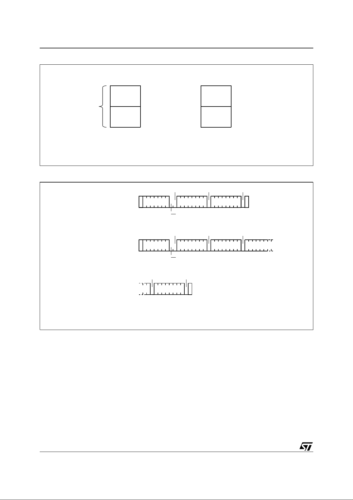
Figure 5. How to Set the Write Protection
FFh
80h
7Fh
00h
Standard
Array
Write
Protected
Array
State of the EEPROM memory
area after write access
to the Protect Register
Memory
Area
Standard
Array
Standard
Array
Default EEPROM memory area
state before write access
to the Protect Register
Figure 6. Write Mode Sequences in the Non Write-Protected Area
ACK ACK ACK
BYTE WRITE DEV SEL BYTE ADDR DATA IN
R/W
START
ACK
PAGE WRITE DEV SEL BYTE ADDR DATA IN 1 DATA IN 2
ACK ACK
FFh
80h
7Fh
00h
AI01936C
STOP
START
ACK ACK
DATA IN N
significant bits only) is incremented. The transfer is
terminated by the master generating a STOP
condition.
When the master generates a STOP condition
immediately after the Ack bi t (in t he “10
th
bit” time
slot), either at the end of a byte write or a page
write, the internal memory write cycle is triggered.
A STOP condition at any other time does not
trigger the internal write cycle.
During the internal write cycle, the SDA input is
disabled internally, and the device does not
respond to any requests.
R/W
STOP
AI01941
Minimizing System Delays by Polling On ACK
During the internal write cycle, the memory
disconnects itself from the bus, and copies the
data from its internal latches to the memory cells.
The maximum write time (t
) is shown in Table 9,
w
but the typical time is shorter. To make use of this,
an Ack polling sequence can be used by the
master.
6/19

Figure 7. Wri te Cy cle Pol l in g Fl owchart using AC K
WRITE Cycle
in Progress
START Condition
DEVICE SELECT
with RW = 0
ACK
NO
Returned
M34C02
First byte of instruction
with RW = 0 already
decoded by M34C02
ReSTART
STOP
YES
Next
Operation is
Addressing the
Memory
WRITE Operation
YESNO
Proceed
Figure 8. Setting the Write Protection Register (WC
BUS ACTIVITY
MASTER
CONTROL
START
BYTE
ADDRESS
= 0)
WORD
Send
Byte Address
DATA
Proceed
Random Address
READ Operation
AI01934
STOP
SDA LINE
BUS ACTIVITY
ACK
DON'T CARE
VALUE
ACK
DON'T CARE
ACK
VALUE
AI01935
7/19

M34C02
The sequence, as shown in Figure 7, is:
– Initial condition: a Write is in progress.
– Step 1: the m aster issues a ST ART condition
followed by a Device Select Code (the first byte
of the new instruction).
– Step 2: if the memory is busy with the inte rnal
write cycle, no Ack will be returned and the
master goes back to Step 1. If the memory has
terminated the internal write cycle, it responds
with an Ack, indicating that the memory is ready
to receive the second part of the next instruction
(the first byte of this instruction having been sent
during Step 1).
Figure 9. Read Mode Sequences
ACK
CURRENT
ADDRESS
READ
RANDOM
ADDRESS
READ
DEV SEL DATA OUT
R/W
START
ACK
DEV SEL * BYTE ADDR
Setting the Protection, Using the Protection
Register
The M34C02 has a software write-protection
function, using the Protecton Register, that allows
the bottom half of the memory area (addresses
00h to 7Fh) to be permanently write protected. The
write protection feature is activated by writing once
to the Protection Register (with the WC
).
at V
SS
input held
The Protection Register is accessed with the
device select code set to 0110b (as shown in
Table 3), and the E2-E1-E0 bits set according to
the states being applied to the E2-E1-E0 pins. As
NO ACK
STOP
ACK ACK
DEV SEL * DATA OUT
NO ACK
SEQUENTIAL
CURRENT
READ
SEQUENTIAL
RANDOM
READ
R/W
START
ACK ACK ACK NO ACK
DEV SEL DATA OUT 1
R/W
START
ACK ACK
DEV SEL * BYTE ADDR
R/W
START
ACK NO ACK
DATA OUT N
STOP
R/W
START
DATA OUT N
ACK ACK
DEV SEL * DATA OUT 1
R/W
START
STOP
STOP
AI01942
Note: 1. The seven most signi ficant bits of the D e vice Select Co de of a Random Read (i n the 1st and 3rd bytes) must be identical.
8/19

M34C02
for any other write command, the WC input needs
to be held at V
. Address and data bytes must be
SS
sent with this command, but their values are all
ignored, and are treated as Don ’t Care. Once the
Protection Register has been written, the write
protection of the first 128 bytes of the memory is
enabled, and it is not pos sible to unprotect t hese
128 bytes, even if the device is powered off and
on, and regardless the state of the WC
input.
When the Protection Register has been written,
the M34C02 no longer responds to the device type
identifier 0110b in either read or write mode.
Read Operations
Read operations are performed independently of
the state of the WC
pin.
Random Address Read
A dummy write is performed to load the address
into the address counter, as shown in Figure 9.
Then,
without
sending a STOP condition, the
master sends another START condition, and
repeats the Device Select Code, with the RW
bit
set to ‘1’. The memory acknowledges this, and
outputs the contents of the addressed byte. The
not
master must
acknowledge the byte output, and
terminates the transfer with a STOP condition.
Current Address Read
The device has an internal address counter which
is incremented each time a byte is read. For the
Current Address Read m ode, following a START
condition, the master sends a Device Select Code
with the RW
bit set to ‘1’. The memory
acknowledges this, and outputs the byte
addressed by the internal address counter. The
counter is then incremented. The master
terminates the transfer with a STOP condition, as
shown in Figure 9,
without
acknowledging the byte
output.
Table 5. 168 Pin DRAM DIMM Connections
DIMM Position
0
1
2
3
4
5
6
7
E2
(pin 167)E1(pin 166)E0(pin 165)
V
VSS V
SS
V
VSS V
SS
V
VCC V
SS
V
VCC V
SS
V
VSS V
CC
V
VSS V
CC
V
VCC V
CC
V
VCC V
CC
SS
CC
SS
CC
SS
CC
SS
CC
Sequenti a l Rea d
This mode can be initiated with either a Current
Address Read or a Random Address Read. The
master
does
acknowledge the data byte output in
this case, and the memory continues to output the
next byte in sequence. To terminate the stream of
not
bytes, the master must
byte output, and
must
acknowledge the last
generate a STOP condition.
The output data comes from consecutive
addresses, with the internal address counter
automatically incremen ted af t er ea ch byt e out put.
After the last memory address, the address
counter ‘rolls-over’ and the memory continues to
output data from address 00h (at the start of the
memory block).
Acknowledge in Read Mode
In all read modes, the memory waits, after each
byte read, for an acknowledgment during the 9
bit time. If the master does n ot pull the SDA line
low during this time, the memory terminates the
data transfer and switches to its standby state.
USE WITHIN A DRAM DIMM
In the application, the M34C02 is soldered directly
in the printed circuit modu le. The 3 C hip Enable
inputs (pins 1, 2 and 3) are connected to pins 165,
166 and 167, respectively, of the 168-pin DRAM
DIMM module. They are wired at V
CC
or V
SS
through the DIMM socket (see Table 5). The SCL
and SDA lines (pins 6 and 5) are connected
respectively to pins 83 and 82 of the memory
module. The pull-up resistors needed for normal
behavior of the I
2
C bus are connected on the I2C
bus of the mother-board (as shown in Figure 10).
The Write Control input of the M34C02 (WC
on pin
7) can be left unconnected. However, connecting
it to V
is recommended, to maintain full read and
SS
write access to the top half of the memory.
Programming the M34C02
When the M34C02 is delivered, full read and write
access is given to the whole memory array. It is
recommended that the first step is t o use the t est
equipment to write the module information (such
as its access speed, i ts size, its organization) to
the first half of the memory, starting from the first
memory location. When the data has been
validated, the test equipment can send a Write
command to the Protection Register, using the
device select code ’01100000b’ followed by an
address and data byte (made up of Don’t Care
values) as shown i n Figu re 8. Th e first 12 8 by tes
of the memory area are then write-protected, and
the M34C02 w ill no longer respond to the s pecif ic
device select code ’0110000xb’. It is not possible
to reverse this sequence.
th
9/19

M34C02
Figure 10. Serial Presence Detect Block Diagram
DIMM Position 7
DIMM Position 6
DIMM Position 5
DIMM Position 4
DIMM Position 3
V
CC
VCCV
V
CC
V
SS
R = 4.7kΩ
SDASCLE0E1E2
V
CC
SDASCLE0E1E2
V
SS
SDASCLE0E1E2
V
CC
SS
SDASCLE0E1E2
V
SS
SDASCLE0E1E2
V
CC
DIMM Position 2
VSSV
DIMM Position 1
V
SS
DIMM Position 0
AI01937
Note: 1. E0, E1 and E2 are wired at each DIMM sock et in a binary sequence for a maxi m um of 8 devices.
2. Common clock and common data are shared across all the devices.
3. Pul l-up resis tors ar e requ ired on all S DA a nd SCL b us li nes ( typic all y 4. 7 k Ω) be ca use t he se li nes ar e o pen dr ain w he n use d as
outputs.
V
SS
CC
V
CC
V
SS
SDASCLE0E1E2
SDASCLE0E1E2
SDASCLE0E1E2
SCL line SDA line
From the motherboard
2
I
C master controller
10/19

M34C02
Table 6. DC Characteristics
(T
= –40 to 85 °C; VCC = 2.5 to 5.5 V, 2.2 to 5.5 V)
A
Symbol Parameter Test Condition Min. Max. Unit
Input Leakage
I
LI
Current
SCL, SDA 0 V ≤ V
IN
≤ V
CC
± 2 µA
I
LO
I
CC
I
CC1
V
IL
V
IH
V
OL
Output Leakage Current 0V ≤ V
V
=5V, fc=400kHz (rise/fall time < 30ns)
CC
V
=2.5V , fc=400kHz (rise/fall time < 30ns)
CC
V
=2.2V , fc=400kHz (rise/fall time < 30ns)
CC
= VSS or V
IN
= VSS or V
IN
V
= VSS or V
IN
Supply Current
Supply Current
(Stand-by)
-W or -L series
-W series
-L series
-W or -L series V
-W series V
-L series
SCL, SDA – 0.3
Input Low
Voltage
E0, E1, E2 – 0.3 0.3V
WC
SCL, SDA 0.7V
Input High
Voltage
E0, E1, E2
WC
Output Low
Voltage
-W or -L series I
-W series I
-L series I
OL
= 2.1 mA, V
OL
= 2.1 mA, V
OL
≤ V
OUT
CC,
CC
CC
CC
= 3 mA, V
SDA in Hi-Z ± 2 µA
2mA
1mA
1mA
, V
= 5 V 1 µA
CC
, V
= 2.5 V 0.5 µA
CC
, V
CC
= 2.2 V
0.5 µA
0.3V
CC
CC
– 0.3 0.5 V
VCC+1 V
CC
0.7V
0.7V
= 5 V 0.4 V
CC
= 2.5 V 0.4 V
CC
= 2.2 V 0.4 V
CC
CC
CC
VCC+1
VCC+1
V
V
V
V
Table 7. AC Measurement Conditions
Input Rise and Fall Times ≤ 50 ns
0.2V
0.3V
to 0.8V
CC
to 0.7V
CC
Input Pulse Voltages
Input and Output Timing
Reference Voltages
CC
CC
Figure 11. AC Testing Input Output Waveforms
0.8V
CC
0.2V
CC
Table 8. Input Parameters 1(TA = 25 °C, f = 400 kHz)
Symbol Parameter Test Condition Min. Max. Unit
C
IN
C
IN
Z
WCL
Z
WCH
t
NS
Note: 1. Sampled only, not 100% tested.
Input Capacitance (SDA) 8 pF
Input Capacitance (other pins) 6 pF
WC Input Impedance VIN < 0.5 V
WC Input Impedance VIN > 0.7V
Low Pass Filter Input Time
Constant (SCL and SDA)
CC
5
500 kΩ
100 500 ns
20 kΩ
0.7V
0.3V
AI00825
CC
CC
11/19

M34C02
Table 9. AC Characteristics
M34C02-W
=2.5 to 5.5V
V
Symbol Alt. Parameter
CC
T
= –40 to 85°C
A
Min Max Min Max
t
CH1CH2
t
CL1CL2
t
DH1DH2
t
DL1DL2
1
t
CHDX
t
CHCL
t
DLCL
t
CLDX
t
CLCH
t
DXCX
t
CHDH
t
DHDL
3
t
CLQV
t
CLQX
f
C
t
W
Note: 1. For a r eS T ART conditio n, o r fo llowing a write cycle.
2. Samp l ed only, not 100 % tested.
3. To avoid spurious START and STOP conditions, a minimum delay is placed between SCL=1 and the falling or rising edge of SDA.
t
Clock Rise Time 300 300 ns
R
t
Clock Fall Time 300 300 ns
F
2
t
SDA Rise Time 20 300 20 300 ns
R
2
t
SDA Fall Time 20 300 20 300 ns
F
t
SU:STA
t
t
HD:STA
t
HD:DAT
t
t
SU:DAT
t
SU:STO
Clock High to Input Transition 600 600 ns
Clock Pulse Width High 600 600 ns
HIGH
Input Low to Clock Low (START) 600 600 ns
Clock Low to Input Transition 0 0 µs
Clock Pulse Width Low 1.3 1.3 µs
LOW
Input Transition to Clock Transition 100 100 ns
Clock High to Input High (STOP) 600 600 ns
t
Input High to Input Low (Bus Free) 1.3 1.3 µs
BUF
t
Clock Low to Data Out Valid 200 900 200 900 ns
AA
t
Data Out Hold Time After Clock Low 200 200 ns
DH
f
Clock Frequency 400 400 kHz
SCL
t
Write Time 10 10 m s
WR
M34C02-L
=2.2 to 5.5V
V
CC
T
= –40 to 85°C
A
Unit
12/19

Figure 12. AC Waveforms
M34C02
SCL
SDA IN
SCL
SDA OUT
SCL
tCHCL
tDLCL
tCHDX
START
CONDITION
tCLQV tCLQX
tCLDX
SDA
INPUT
DATA VALID
DATA OUTPUT
SDA
CHANGE
tW
tCLCH
tDXCX
tCHDH
tDHDL
STOP &
BUS FREE
SDA IN
tCHDH
STOP
CONDITION
WRITE CYCLE
tCHDX
START
CONDITION
AI00795B
13/19

M34C02
Table 10. Ordering Information Scheme
Example: M34C02 –W MN 6 T
Operating Voltage Option
W 2.5 V to 5.5 V T Tape and Reel Packing
L 2.2 V to 5.5 V
Package Temperature Range
PSDIP8 (0.25 mm
1
BN
frame)
MN SO8 (150 mil width)
DW TSSOP8 (169 mil width)
Note: 1. Packa ge-type available only on request.
6 –40 °C to 85 °C
ORDERING INFORMATION
Devices are shipped from the factory with the
memory content set at all ‘1’s (FFh), and the
Protection Register set at all ‘0’s (00h).
The notation used for the device number is as
shown in Table 10. For a list of available options
(speed, package, etc.) or for further information on
any aspect of this device, please contact your
nearest ST Sales Office.
14/19

Table 11. PSDIP8 - 8 pin Plastic Skinny DIP, 0.25mm lead frame
mm inches
Symb.
Typ. Min. Max. Typ. Min. Max.
A 3.90 5 .90 0.154 0.232
A1 0.49 – 0.019 –
A2 3.30 5.30 0.130 0.209
B 0.36 0 .56 0.014 0.022
B1 1.15 1.65 0.045 0.065
C 0.20 0.36 0.008 0.014
D 9.20 9.90 0.362 0.390
E 7.62 – – 0.300 – –
E1 6.00 6.70 0.236 0.264
e1 2.54 – – 0. 100 – –
eA 7.80 – 0.307 –
eB 10.00 0.394
L 3.00 3.80 0.118 0.150
M34C02
N8 8
Figure 13. PSDIP8 (BN)
A2
A1AL
B
N
1
e1
B1
D
E1 E
eA
eB
C
PSDIP-a
Note: 1. D rawing is not to sc al e.
15/19

M34C02
Table 12. SO8 - 8 lead Plastic Small Outline, 150 mils body width
Symb.
Typ. Min. Max. Typ. Min. Max.
A 1.35 1 .75 0.053 0.069
A1 0.10 0.25 0.004 0.010
B 0.33 0 .51 0.013 0.020
C 0.19 0.25 0.007 0.010
D 4.80 5.00 0.189 0.197
E 3.80 4 .00 0.150 0.157
e 1 .27 – – 0.050 – –
H 5.80 6.20 0.228 0.244
h 0.25 0.50 0.010 0.020
L 0.40 0.90 0.016 0.035
α 0° 8° 0° 8°
N8 8
CP 0.10 0.004
mm inches
Figure 14. SO8 narrow (MN)
B
SO-a
Note: 1. D rawing is not to sc al e.
h x 45˚
A
e
D
N
1
CP
E
H
C
LA1 α
16/19

Table 13. TSSOP8 - 8 lead Thin Shrink Small Outline
mm inches
Symb.
Typ. Min. Max. Typ. Min. Max.
A 1.10 0.043
A1 0.05 0.15 0.002 0.006
A2 0.85 0.95 0.033 0.037
B 0.19 0.30 0.007 0.012
C 0.09 0.20 0.004 0.008
D 2.90 3.10 0.114 0.122
E 6.25 6.50 0.246 0.256
E1 4.30 4.50 0.169 0.177
e 0.65 – – 0.026 – –
L 0.50 0.70 0.020 0.028
α 0° 8° 0° 8°
N8 8
CP 0.08 0.003
M34C02
Figure 15. TSSOP8 (DW)
CP
Note: 1. D rawing is not to sc al e.
D
A1
DIE
C
α
L
TSSOP
N
EE1
1
N/2
A2A
eB
17/19

M34C02
Table 14. Revision History
Date Description of Revision
27-Dec-1999
Adjustments to the formatting. 0 to 70°C temperature range removed from DC and AC tables.
No change to description of device, or parameters
18/19

M34C02
Information furnished is believed to be accurate and reliable. However, STMicroelectronics assumes no responsibility for the consequences
of use of such information nor for any infringement of patents or other rights of third parties which may result from its use. No license is granted
by implic ation or otherw i se under any patent or pat ent rights of S T M i croelectronics. Specific ations mentioned in this p ublication are subject
to change without notice. This publication supersedes and replaces all information previously supplied. STMicroelectronics products are not
authorized for use as criti cal components in l i f e support device s or systems without express writ t en approval of STMi croelectronics.
© 1999 STMicroelectronics - All Rights Reserved
The ST logo is a registered t rademark of STMi croelectronic s.
All other na m es are the proper ty of their respectiv e owners.
STMicroelectronics GROUP OF COMPANIES
Australia - Brazil - China - Finland - France - Germany - Hong Kong - India - Italy - Japan - Malaysia - Malta - Morocco - Singapore - Spain -
Sweden - Switzerland - United Kingdom - U.S.A.
http://www.s t. com
19/19
 Loading...