

ST M29W400T, M29W400B User Manual
查询M29W400供应商
4 Mbit (512Kb x8 or 256Kb x16, Boot Block)
Low Voltage Single Supply Flash Memory
M29W400Tand M29W400Bare replaced
respectivelyby theM29W400BT and
M29W400BB
2.7Vto 3.6V SUPPLYVOLTAGE for
PROGRAM,ERASE and READ OPERATIONS
FASTACCESSTIME:90ns
FASTPROGRAMMINGTIME
–10µs by Byte /16µs by Word typical
PROGRAM/ERASECONTROLLER(P/E.C.)
– Program Byte-by-Byte or Word-by-Word
– Status Register bits andReady/BusyOutput
MEMORYBLOCKS
– Boot Block(Top or Bottom location)
– Parameter and Main blocks
BLOCK,MULTI-BLOCK and CHIP ERASE
MULTI BLOCKPROTECTION/TEMPORARY
UNPROTECTION MODES
ERASESUSPENDand RESUME MODES
– Read and Programanother Block during
EraseSuspend
LOWPOWER CONSUMPTION
– Stand-by and AutomaticStand-by
100,000PROGRAM/ERASECYCLES per
BLOCK
20YEARSDATARETENTION
– Defectivity below 1ppm/year
ELECTRONICSIGNATURE
– ManufacturerCode: 0020h
– Device Code, M29W400T:00EEh
– Device Code, M29W400B: 00EFh
DESCRIPTION
The M29W400 is a non-volatilememory that may
be erasedelectricallyat theblock or chipleveland
programmedin-systemon a Byte-by-ByteorWordby-Wordbasisusing onlya single2.7Vto3.6V V
supply. For Program and Erase operations the
necessary high voltages are generated internally.
The device can also be programmed in standard
programmers.
The arraymatrixorganisationallowseach block to
be erased and reprogrammed without affecting
other blocks. Blockscan be protectedagainstprograming and erase on programming equipment,
CC
12 x 20 mm
BGA
FBGA48 (ZA)
8 x 6 solder balls
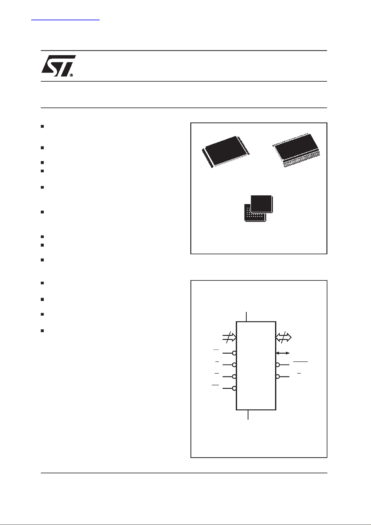
Figure 1. LogicDiagram
V
CC
18
A0-A17
W
E
G
RP
M29W400T
M29W400B
V
SS
M29W400T
M29W400B
NOT FOR NEW DESIGN
44
1
SO44 (M)TSOP48 (N)
15
DQ0-DQ14
DQ15A–1
BYTE
RB
AI02065
November 1999 1/34
This isinformationona product stillin productionbut not recommendedfor newdesigns.
M29W400T, M29W400B
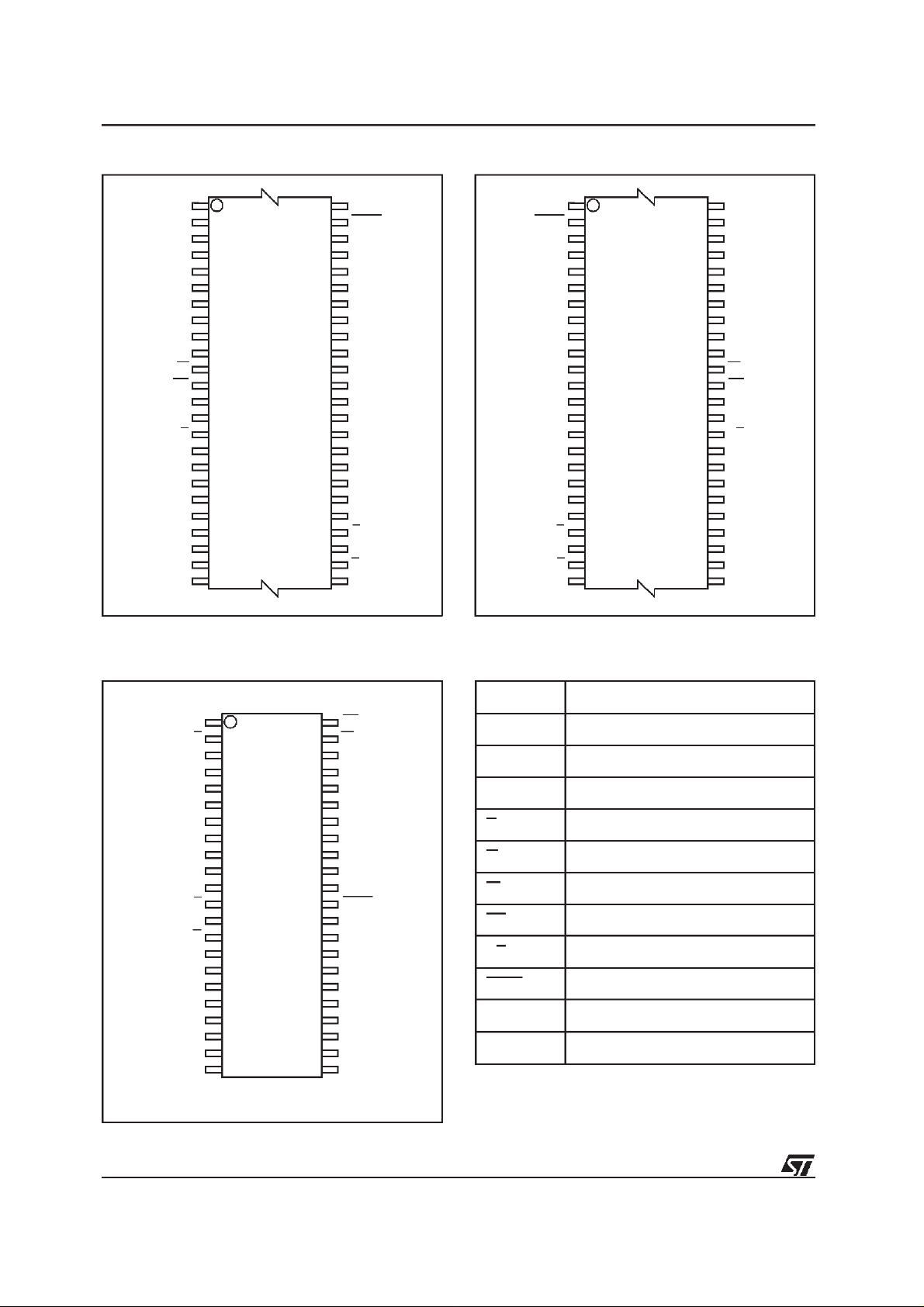
Figure 2A. TSOP Pin Connections
A15
1
A14
A13
A12
A11
A10 DQ14
A9
A8
NC
NC
W
RP
NC
NC
RB
NC
A17
A7
A6
A5
A4
A3
A2
A1
M29W400T
12
M29W400B
13
(Normal)
24 25
48
37
36
AI02066
A16
BYTE
V
SS
DQ15A–1
DQ7
DQ6
DQ13
DQ5
DQ12
DQ4
V
CC
DQ11
DQ3
DQ10
DQ2
DQ9
DQ1
DQ8
DQ0
G
V
SS
E
A0
Figure 2B. TSOP ReversePin Connections
A16
BYTE
V
SS
DQ15A–1
DQ7
DQ14
DQ6
DQ13
DQ5
DQ12
DQ4
V
CC
DQ11
DQ3
DQ10
DQ2
DQ9
DQ1
DQ8
DQ0
V
SS
A0
1
M29W400T
12
M29W400B
13
(Reverse)
G
E
24 25
AI02067
48
37
36
A15
A14
A13
A12
A11
A10
A9
A8
NC
NC
W
RP
NC
NC
RB
NC
A17
A7
A6
A5
A4
A3
A2
A1
Warning: NC = Not Connected. Warning: NC = Not Connected.
Figure 2C. SO Pin Connections
Table1. Signal Names
A0-A17 Address Inputs
NC RP
1
2
3
A17 A8
A7
4
5
A6
6
A5
A4
7
A3
8
A2
9
A1
10
A0
11
M29W400T
M29W400B
12
13
14
15
16
17DQ1
18
19
20
21
V
SS
DQ0
DQ8
DQ9
DQ10
DQ3
DQ11
E
G
44
43
42
41
40
39
38
37
36
35
34
33
32
31
30
29
28
27
26
25
24
2322
AI02068
WRB
A9
A10
A11
A12
A13
A14
A15
A16
BYTE
V
SS
DQ15A–1
DQ7
DQ14
DQ6
DQ13
DQ5DQ2
DQ12
DQ4
V
CC
DQ0-DQ7 Data Input/Outputs,Command Inputs
DQ8-DQ14 Data Input/Outputs
DQ15A–1 Data Input/Outputor Address Input
E Chip Enable
G Output Enable
W Write Enable
RP Reset /Block TemporaryUnprotect
RB Ready/Busy Output
BYTE Byte/Word Organisation
V
CC
V
SS
Supply Voltage
Ground
Warning: NC = Not Connected.
2/34
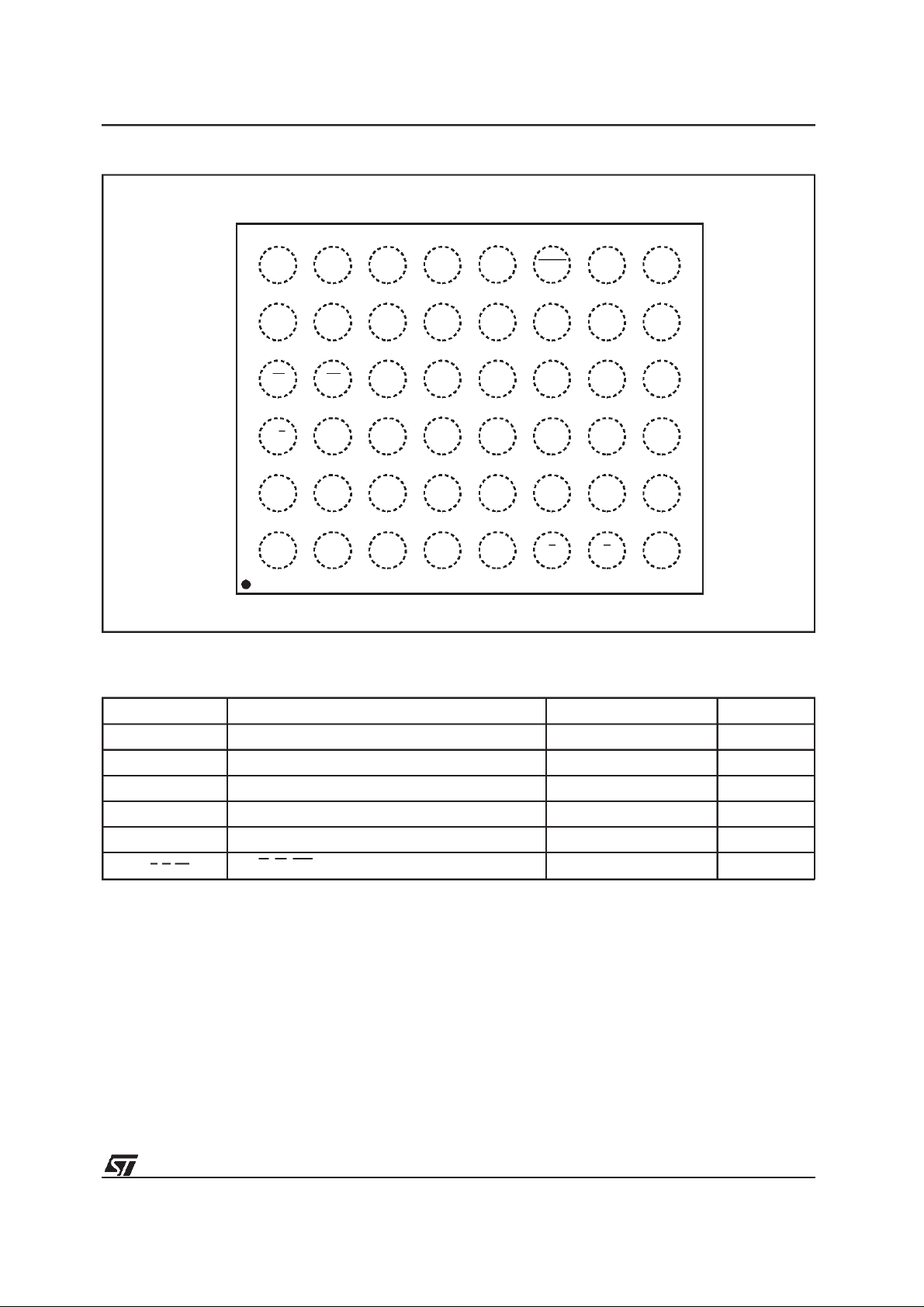
Figure 2D. FBGA Package Ball Out (Top View)
M29W400T, M29W400B
87654321
F
E
D
C
B
A
A4A3
Warning: NC = Not Connected.
Table2. AbsoluteMaximumRatings
A15A14A12A13
A11 DQ7
NC
A2 V
(1)
A5
A1
A16
DQ2
BYTE
DQ12DQ5NCNCRPW
DQ15
A–1
CC
GEA0
V
SS
DQ6DQ13DQ14A10A8A9
DQ4V
DQ3DQ11DQ10NCNCRB
DQ1DQ9DQ8DQ0A6A17A7
SS
AI00912
Symbol Parameter Value Unit
T
A
T
BIAS
T
STG
(2)
V
IO
V
CC
V
(A9, E, G, RP)
Notes: 1. Except for the rating ”Operating TemperatureRange”, stresses above those listedin theTable ”Absolute Maximum Ratings”
may cause permanent damage to the device. These are stress ratings only and operationof the device atthese or any other
conditions above those indicated in the Operating sections of this specification is notimplied. Exposure to AbsoluteMaximum
Rating conditions for extended periods may affect device reliability. Referalso to the STMicroelectronics SURE Program and other
relevant qualitydocuments.
2. Minimum Voltagemay undershootto–2V duringtransition and for less than 20ns.
3. Depends on range.
Ambient Operating Temperature
TemperatureUnder Bias –50 to125 °C
Storage Temperature –65 to150 °C
Input or OutputVoltages –0.6 to 5 V
Supply Voltage –0.6 to 5 V
(2)
A9, E, G, RP Voltage –0.6to 13.5 V
DESCRIPTION(Cont’d)
and temporarily unprotected to make changes in
the application. Each block can be programmed
and erasedover 100,000 cycles.
Instructions for Read/Reset,Auto Selectfor reading the Electronic Signature or Block Protection
(3)
–40 to85 °C
Suspend and Resumeare writtento the devicein
cyclesofcommandstoa CommandInterfaceusing
standardmicroprocessor write timings.
The device is offered in TSOP48 (12 x 20mm),
SO44 and FBGA48 (8 x 6 balls, 0.8mm pitch)
packages. Both normal and reverse pinouts are
availablefor the TSOP48 package.
status,Programming,BlockandChipErase,Erase
3/34
M29W400T, M29W400B
Figure 3. MemoryMap and Block Address Table(x8)
7FFFFh
7C000h
7BFFFh
7A000h
79FFFh
78000h
77FFFh
70000h
6FFFFh
60000h
5FFFFh
50000h
4FFFFh
40000h
3FFFFh
30000h
2FFFFh
20000h
1FFFFh
10000h
0FFFFh
00000h
M29W400T
16K BOOT BLOCK
8K PARAMETER BLOCK
8K PARAMETER BLOCK
32K MAIN BLOCK
64K MAIN BLOCK
64K MAIN BLOCK
64K MAIN BLOCK
64K MAIN BLOCK
64K MAIN BLOCK
64K MAIN BLOCK
64K MAIN BLOCK
7FFFFh
70000h
6FFFFh
60000h
5FFFFh
50000h
4FFFFh
40000h
3FFFFh
30000h
2FFFFh
20000h
1FFFFh
10000h
0FFFFh
08000h
07FFFh
06000h
05FFFh
04000h
03FFFh
00000h
M29W400B
64K MAIN BLOCK
64K MAIN BLOCK
64K MAIN BLOCK
64K MAIN BLOCK
64K MAIN BLOCK
64K MAIN BLOCK
64K MAIN BLOCK
32K MAIN BLOCK
8K PARAMETER BLOCK
8K PARAMETER BLOCK
16K BOOT BLOCK
AI02090
Organisation
The M29W400 is organised as 512K x8 or 256K
x16 bits selectable by the BYTE signal. When
BYTE is Low the Byte-wide x8 organisation is
selected and the address lines are DQ15A–1 and
A0-A17. The Data Input/Output signal DQ15A–1
actsasaddresslineA–1 whichselectstheloweror
upper Byte of the memory word for output on
DQ0-DQ7,DQ8-DQ14remainat High impedance.
When BYTEis Highthe memory usestheaddress
inputs A0-A17 and the Data Input/Outputs DQ0DQ15.Memorycontrol is provided by ChipEnable
E, Output Enable G andWrite Enable W inputs.
AReset/BlockTemporaryUnprotection RPtri-level
input providesa hardware reset when pulled Low,
andwhenheld High(atV
) temporarily unprotects
ID
blocks previously protected allowing them to be
programedanderased.Erase andProgramoperations are controlled by an internal Program/Erase
Controller(P/E.C.).StatusRegisterdataoutput on
DQ7 providesa DataPolling signal,and DQ6and
DQ2 provideTogglesignalstoindicatethe state of
the P/E.C operations. A Ready/Busy RB output
indicatesthe completion of the internalalgorithms.
4/34
MemoryBlocks
The devices featureasymmetrically blockedarchitectureprovidingsystem memoryintegration.Both
M29W400Tand M29W400Bdeviceshaveanarray
of 11 blocks, one Boot Block of 16 KBytes or 8
KWords, two Parameter Blocks of 8 KBytes or 4
KWords, one Main Block of 32 KBytes or 16
KWordsand sevenMainBlocksof64KBytesor32
KWords.TheM29W400Thasthe BootBlockatthe
top of the memory ad dress spa ce and the
M29W400B locates the Boot Block startingat the
bottom. The memory maps are showed in Figure
3. Each block can beerased separately,any combination of blocks can be specifiedfor multi-block
eraseor the entirechip may be erased. The Erase
operations are managed automatically by the
P/E.C. The block erase operation can be suspended in order to read from or program to any
blocknot beingersased, and then resumed.
Block protection provides additional data security.
Each block can be separatelyprotected or unprotected against Program or Eraseon programming
equipment. All previously protected blocks can be
temporarilyunprotected in theapplication.
M29W400T, M29W400B
Table3A. M29W400TBlock Address Table
Address Range (x8) Address Range(x16) A17 A16 A15 A14 A13 A12
00000h-0FFFFh 00000h-07FFFh 0 0 0 X X X
10000h-1FFFFh 08000h-0FFFFh 0 0 1 X X X
20000h-2FFFFh 10000h-17FFFh 0 1 0 X X X
30000h-3FFFFh 18000h-1FFFFh 0 1 1 X X X
40000h-4FFFFh 20000h-27FFFh 1 0 0 X X X
50000h-5FFFFh 28000h-2FFFFh 1 0 1 X X X
60000h-6FFFFh 30000h-37FFFh 1 1 0 X X X
70000h-77FFFh 38000h-3BFFFh 1110XX
78000h-79FFFh 3C000h-3CFFFh 111100
7A000h-7BFFFh 3D000h-3DFFFh 111101
7C000h-7FFFFh 3E000h-3FFFFh 11111X
Table3B. M29W400BBlock AddressTable
Address Range (x8) Address Range(x16) A17 A16 A15 A14 A13 A12
00000h-03FFFh 00000h-01FFFh 00000X
04000h-05FFFh 02000h-02FFFh 000010
06000h-07FFFh 03000h-03FFFh 000011
08000h-0FFFFh 04000h-07FFFh 0001XX
10000h-1FFFFh 08000h-0FFFFh 0 0 1 X X X
20000h-2FFFFh 10000h-17FFFh 0 1 0 X X X
30000h-3FFFFh 18000h-1FFFFh 0 1 1 X X X
40000h-4FFFFh 20000h-27FFFh 1 0 0 X X X
50000h-5FFFFh 28000h-2FFFFh 1 0 1 X X X
60000h-6FFFFh 30000h-37FFFh 1 1 0 X X X
70000h-7FFFFh 38000h-3FFFFh 1 1 1 X X X
Bus Operations
The following operations can be performed using
the appropriatebuscycles:Read (Array, Electronic
Signature, Block Protection Status), Write com-
mand,Output Disable, Standby,Reset, BlockProtection, Unprotection, Protection Verify, Unprotection VerifyandBlockTemporaryUnprotection.See
Tables4 and 5.
5/34

M29W400T, M29W400B
Command Interface
Instructions,made up of commandswritten in cycles, canbe giventotheProgram/EraseController
through a Command Interface (C.I.). For added
data protection,program or eraseexecutionstarts
after4or6cycles.Thefirst,second,fourthandfifth
cycles are used to input Coded cycles to the C.I.
This Coded sequence is the same for all Program/Erase Controller instructions. The ’Command’itself and its confirmation,when applicable,
are givenon the third,fourth or sixth cycles. Any
incorrectcommand orany improper command sequence will reset the device to ReadArray mode.
Instructions
Seven instructions are defined to perform Read
Array,AutoSelect(toreadtheElectronicSignature
or BlockProtectionStatus),Program, BlockErase,
Chip Erase, Erase Suspend and Erase Resume.
The internal P/E.C. automaticallyhandles all timing and verification of the Program and Erase
operations.The Status RegisterData Polling,Toggle, Error bits and the RB output may be read at
any time, duringprogrammingor erase,tomonitor
the progress of the operation.
Instructionsare composed of upto sixcycles. The
first two cycles input a Coded sequence to the
CommandInterfacewhichis commontoallinstructions (see Table 8). The third cycle inputs the
instruction set-up command. Subsequent cycles
output theaddressed data,ElectronicSignatureor
Block Protection Status for Read operations. In
ordertogiveadditionaldataprotection,the instructions for Program and Block or Chip Erase require
furthercommandinputs.ForaPrograminstruction,
the fourth command cycle inputs the address and
data to be programmed. For an Erase instruction
(Block or Chip), the fourth and fifth cycles input a
further Coded sequence before the Eraseconfirm
commandon thesixthcycle. Erasureof a memory
blockmaybe suspended,in ordertoreaddatafrom
another block or to programdata in another block,
and thenresumed.
When power is first applied or if V
, the command interface is reset to Read
V
LKO
falls below
CC
Array.
SIGNALDESCRIPTIONS
See Figure 1 andTable1.
AddressInputs (A0-A17). The addressinputs for
the memoryarrayare latchedduringawriteoperation on the falling edge of Chip Enable E or Write
Enable W. InWord-wide organisationthe address
lines are A0-A17, in Byte-wide organisation
DQ15A–1acts as an additional LSB addressline.
WhenA9 is raised to V
, either a ReadElectronic
ID
Signature Manufacturer or Device Code, Block
Protection Status or a Write Block Protection or
Block Unprotection is enabled depending on the
combinationoflevelson A0,A1, A6, A12 andA15.
Data Input/Outputs (DQ0-DQ7). These Inputs/Outputsare used in the Byte-wideand Wordwide organisations. The input is data to be
programmed in the memory array or a command
to be written to the C.I. Both are latched on the
rising edge of Chip Enable E or Write Enable W.
The output is data from the Memory Array, the
Electronic Signature Manufacturer or Device
codes, the Block Protection Status or the Status
registerData Pollingbit DQ7,the Toggle Bits DQ6
and DQ2, the Errorbit DQ5or the EraseTimer bit
DQ3. Outputs are valid when Chip Enable E and
Output Enable G are active. The output is high
impedance when the chip is deselected or the
outputsaredisabledandwhen RPisat aLowlevel.
Data Input/Outputs (DQ8-DQ14 and DQ15A–1).
These Inputs/Outputsare additionallyused in the
Word-wideorganisation.WhenBYTEisHighDQ8DQ14 and DQ15A–1 act as the MSB of the Data
Inputor Output, functioningas describedfor DQ0DQ7 above, and DQ8-DQ15 are ’don’t care’ for
commandinputsor status outputs.When BYTEis
Low,DQ8-DQ14are highimpedance,DQ15A–1is
the AddressA–1 input.
Chip Enable (E). The Chip Enableinput activates
the memory control logic, input buffers, decoders
andsenseamplifiers.EHighdeselectsthememory
andreducesthepowerconsumptiontothestandby
level. E can also be used to controlwriting to the
commandregister and to thememory array, while
Wremainsata lowlevel.TheChipEnablemust be
forcedto V
duringthe BlockUnprotectionopera-
ID
tion.
6/34

M29W400T, M29W400B
Output Enable (G). The Output Enable gates the
outputs through the data buffers during a read
operation. When G is High the outputs are High
impedance. G must be forced to V
level during
ID
Block Protection andUnprotectionoperations.
WriteEnable(W). Thisinput controlswriting tothe
CommandRegisterandAddressandDatalatches.
Byte/Word Organization Select (BYTE). The
BYTEinputselects theoutput configurationforthe
device: Byte-wide (x8) mode or Word-wide (x16)
mode. When BYTEis Low,the Byte-widemode is
selectedand the data is read and programmedon
DQ0-DQ7. In this mode, DQ8-DQ14 are at high
impedance and DQ15A–1 is the LSB address.
When BYTE is High, the Word-wide mode is selected and the data is read and programmed on
DQ0-DQ15.
Ready/Busy Output (RB). Ready/Busy is an
open-drainoutputandgivestheinternalstateofthe
P/E.C. of the device. When RB is Low, the device
is Busy with a Programor Erase operation and it
will not accept any additional program or erase
instructionsexcept the Erase Suspendinstruction.
WhenRB isHigh,thedeviceisreadyforanyRead,
Program or Erase operation. The RB will also be
High when the memoryis putin EraseSuspendor
Standby modes.
Reset/Block Temporary Unprotect Input (RP).
The RP Input provides hardware reset and protected block(s) temporary unprotection functions.
Reset of the memory is acheivedby pulling RPto
for atleastt
V
IL
.When thereset pulseis given,
PLPX
if the memory is in Read or Standby modes, it will
be available for new operations in t
PHEL
after the
rising edgeofRP.Ifthememoryis in Erase,Erase
Suspend or Program modes the reset will take
duringwhichtheRB signal will beheldatVIL.
t
PLYH
The end of the memory reset will be indicated by
the rising edge of RB. Ahardwareresetduring an
Erase or Program operation will corrupt the data
being programmed or the sector(s) being erased
(see Table14 andFigure9).
Temporary block unprotectionis made by holding
RP at V
. In this condition previously protected
ID
blocks can be programmedor erased.The transitionof RPfromV
When RP is returned from V
toVIDmustslower thant
IH
to VIHall blocks
ID
PHPHH
temporarily unprotected will be again protected.
See Table15 andFigure9.
V
Supply Voltage. The power supply for all
CC
operations (Read,Programand Erase).
Ground. VSSis the reference for all voltage
V
SS
measurements.
DEVICEOPERATIONS
See Tables 4, 5and 6.
Read. Read operations are used to output the
contents of the MemoryArray, the ElectronicSignature,the StatusRegister orthe BlockProtection
Status. Both Chip Enable E and Output Enable G
must be low in order to read the output of the
memory.
Write.Writeoperationsareused togiveInstruction
Commandsto thememory orto latchinputdatato
beprogrammed.Awriteoperationis initiatedwhen
Chip Enable E is Lowand Write Enable W is Low
withOutput EnableGHigh.Addressesare latched
onthefallingedgeof Wor E whicheveroccurslast.
CommandsandInputDataarelatchedontherising
edge of W orE whichever occursfirst.
OutputDisable. Thedata outputsare highimpedance whenthe OutputEnable G isHigh with Write
EnableW High.
Standby. The memory is in standby when Chip
EnableEis Highand theP/E.C. is idle.The power
consumption is reduced to the standby level and
the outputs are high impedance, independentof
the Output Enable G or Write EnableWinputs.
Automatic Standby. After 150ns of bus inactivity
and whenCMOSlevels are driving theaddresses,
the chip automatically enters a pseudo-standby
modewhere consumptionisreducedto the CMOS
standbyvalue, whileoutputs still drivethe bus.
Electronic Signature. Two codes identifyingthe
manufacturer andthedevicecanberead fromthe
memory. The manufacturer’s code for STMicroelectronics is 20h, the device code is EEh for
the M29W400T (Top Boot) and EFh for the
M29W400B(BottomBoot).Thesecodesallowprogramming equipment or applications to automaticallymatch their interfaceto thecharacteristicsof
the M29W400. The ElectronicSignature is output
by a Read operationwhen the voltage applied to
A9 is at V
and address inputs A1 is Low. The
ID
manufacturer code is output when the Address
input A0 is Low and the device code when this
input is High. Other Address inputs are ignored.
The codesare output on DQ0-DQ7.
.
TheElectronicSignaturecan also beread,without
raisingA9toV
, by givingthe memorythe Instruc-
ID
tion AS. If the Byte-wide configuration is selected
thecodesareoutputon DQ0-DQ7withDQ8-DQ14
at High impedance; if the Word-wideconfiguration
is selectedthe codes are outputon DQ0-DQ7with
DQ8-DQ15at 00h.
7/34
M29W400T, M29W400B
Table4. User Bus Operations
(1)
Operation E G W RP BYTE A0 A1 A6 A9 A12 A15
V
V
V
Read Word V
Read Byte V
Write Word V
Write Byte V
OutputDisable V
Standby V
ILVIL
ILVIL
ILVIH
ILVIH
ILVIH
XXVIHX X X X X X X Hi-Z Hi-Z Hi-Z
IH
IH
V
IH
V
IL
V
IL
V
IH
Reset X X X V
Block
Protection
Blocks
Unprotection
Block
Protection
Verify
Block
Unprotection
Verify
Block
Temporary
Unprotection
Notes: 1. X = V
(2,4)
(2,4)
(2,4) V
ILVIDVIL
VIDVIDVILPulse V
(4)
VILV
VILV
Pulse V
V
IL
IH
V
IL
IH
XX X V
orV
IL
2. Block Address must be given on A12-A17 bits.
3. See Table 6.
IH
IH
V
IH
V
IH
V
IH
V
IH
IL
IH
IH
V
IH
V
IH
ID
A0 A1 A6 A9 A12 A15
IH
V
A0 A1 A6 A9 A12 A15
IL
V
A0 A1 A6 A9 A12 A15 Data Input Data Input
IH
V
A0 A1 A6 A9 A12 A15
IL
X X X X X X X Hi-Z Hi-Z Hi-Z
X X X X X X X Hi-Z Hi-Z Hi-Z
XXXXVIDXX X X X
XXXXVIDVIHV
XVILVIHVILVIDA12 A15 X X
XVILVIHVIHVIDA12 A15 X X
X XXXXXX X X X
4. Operation performed on programming equipment.
IH
DQ15
A–1
Data
Output
Address
Input
Address
Input
DQ8-
DQ14
Data
Output
Hi-Z
Hi-Z
DQ0-DQ7
Data
Output
Data
Output
Data
Input
Data
Input
XXX
Block
Protect
Status
Block
Protect
Status
(3)
(3)
Table5. Read Electronic Signature(following AS instruction or with A9 = VID)
Org. Code Device E G W BYTE A0 A1
Word-
wide
Manufact.
Code
Device
Code
Manufact.
Code
M29W400T V
M29W400B V
V
VILV
IL
VILV
IL
VILV
IL
VILV
V
IL
V
IH
V
IH
V
IH
V
IH
VILVILDon’t Care 0 00h 20h
IH
V
IH
IH
IL
IH
V
IH
V
IL
Byte-
wide
Device
M29W400T V
IL
VILV
V
IH
V
IL
IH
Code
M29W400B V
IL
VILV
V
IH
V
IL
IH
Other
Addresses
VILDon’t Care 0 00h EEh
VILDon’t Care 0 00h EFh
VILDon’t Care
VILDon’t Care
VILDon’t Care
DQ15
A–1
Don’t
Care
Don’t
Care
Don’t
Care
Table6. Read Block Protectionwith AS Instruction
Code E G W A0 A1 A12-A17
Protected Block V
Unprotected Block V
IL
IL
V
IL
V
IL
V
IH
V
IH
V
IL
V
IL
V
IH
V
IH
Block Address Don’t Care 01h
Block Address Don’t Care 00h
Addresses
Other
DQ8-
DQ14
DQ0-
DQ7
Hi-Z 20h
Hi-Z EEh
Hi-Z EFh
DQ0-DQ7
8/34
M29W400T, M29W400B
Table7. Commands
Hex Code Command
00h Invalid/Reserved
10h Chip Erase Confirm
20h Reserved
30h Block Erase Resume/Confirm
80h Set-up Erase
90h
A0h Program
B0h Erase Suspend
F0h Read Array/Reset
Read Electronic Signature/
Block Protection Status
Block Protection. Each block can be separately
protected against Program or Erase on programming equipment. Block protection provides additional data security, as it disables all program or
eraseoperations.Thismodeis activatedwhenboth
A9 and G are raised to V
and anaddress in the
ID
block is applied on A12-A17.The Block Protection
algorithmis showninFigure14. Blockprotectionis
initiated on theedge of W falling to V
a delayof 100µs, the edge ofW risingto V
. Then after
IL
IH
ends
the protectionoperations.Block protectionverifyis
achievedby bringingG, E, A0andA6to V
toV
, whileW is at VIHandA9 atVID. Underthese
IH
andA1
IL
conditions,reading thedata output will yield 01h if
the block defined by the inputs on A12-A17 is
protected.Any attempt to program or erase aprotected block will be ignoredby the device.
Block Temporary Unprotection. Any previously
protected block canbe temporarilyunprotectedin
ordertochangestoreddata.Thetemporaryunprotection mode is activated by bringing RP to V
ID
During the temporary unprotectionmode the previously protected blocks are unprotected. A block
can be selected and data can be modified by
executingtheEraseorPrograminstructionwiththe
RP signalheldat V
. When RP is returnedto VIH,
ID
all the previously protected blocks are again protected.
Block Unprotection. All protected blocks can be
unprotected on programming equipment to allow
updating of bit contents. All blocks must first be
protectedbefore the unprotectionoperation.Block
unprotectionis activatedwhen A9, G and E areat
and A12,A15 at VIH. The Block Unprotection
V
ID
algorithm is shown in Figure 15. Unprotection is
initiatedbythe edgeof Wfallingto V
.Aftera delay
IL
of 10ms, the unprotectionoperation will end. Unprotectionverifyis achievedby bringingG and E to
whileA0 is atVIL, A6 andA1are at VIHandA9
V
IL
remains at V
. In these conditions, reading the
ID
outputdatawillyield00h if theblockdefinedbythe
inputsA12-A17has beensuccesfullyunprotected.
Eachblockmustbe separatelyverifiedbygivingits
address in order to ensurethatit has been unprotected.
INSTRUCTIONS AND COMMANDS
The Command Interface latches commands written to the memory. Instructions are made up from
one or morecommands to performRead Memory
Array,Read ElectronicSignature,Read Block Protection, Program, Block Erase, Chip Erase, Erase
Suspend and Erase Resume. Commands are
made of address and data sequences. The instructionsrequirefrom 1to6 cycles,the firstor first
threeof whichare alwayswrite operations used to
initiatethe instruction. They are followedby either
furtherwrite cyclesto confirmthe firstcommandor
executethe commandimmediately.Command sequencing must be followed exactly. Any invalid
combinationof commands will reset the device to
Read Array. The increased number of cycles has
been chosen to assure maximum data security.
.
Instructionsare initialised by two initial Coded cycleswhich unlockthe CommandInterface.In addition, for Erase, instruction confirmation is again
precededby the two Coded cycles.
9/34
M29W400T, M29W400B
Table8. Instructions
Mne. Instr. Cyc. 1st Cyc. 2nd Cyc. 3rd Cyc. 4th Cyc. 5th Cyc. 6th Cyc. 7th Cyc.
(2,4) Read/Reset
RD
ES
Notes:
Memory Array
(4)
Auto Select 3+
AS
PG Program 4
BE Block Erase 6
CE Chip Erase 6
(10) Erase
Suspend
Erase
ER
Resume
1. Commands not interpreted in this tablewill default to read array mode.
2. Await of t
before startingany new operation (see Table14 andFigure 9).
3. X = Don’tCare.
4. The first cycles of the RD orAS instructions are followed by read operations. Any number of read cycles can occur after
the commandcycles.
5. SignatureAddress bits A0,A1 at V
Device code.
6. Block Protection Address: A0 atV
7. For Codedcycles address inputs A15-A17are don’t care.
8. Optional, additional Blocks addresses must be enteredwithin the erase timeout delay after last write entry, timeoutstatus
can beverified through DQ3 value (see Erase TimerBit DQ3 description). Whenfull commandis entered, read Data Polling or
Togglebit until Erase is completed or suspended.
9. Read DataPolling, Toggle bits or RB until Erase completes.
10.During Erase Suspend,Read and Data Program functions are allowed in blocks not being erased.
PLYH
(1)
(3,7)
Addr.
1+
Data F0h
Byte AAAAh 5555h AAAAh
(3,7)
Addr.
3+
Data AAh 55h F0h
Addr.
Data AAh 55h 90h
Addr.
Data AAh 55h A0h
Addr.
Data AAh 55h 80h AAh 55h 30h 30h
Addr.
Data AAh 55h 80h AAh 55h 10h
Addr.
1
Data B0h
Addr.
1
Data 30h
is necessary after a Read/Resetcommand if the memorywas in an Erase or Program mode
Word 5555h 2AAAh 5555h
Byte AAAAh 5555h AAAAh
(3,7)
Word 5555h 2AAAh 5555h
Byte AAAAh 5555h AAAAh
(3,7)
Word 5555h 2AAAh 5555h
Byte AAAAh 5555h AAAAh AAAAh 5555h
(3,7)
Word 5555h 2AAAh 5555h 5555h 2AAAh
Byte AAAAh 5555h AAAAh AAAAh 5555h AAAAh
(3,7)
Word 5555h 2AAAh 5555h 5555h 2AAAh 5555h
(3,7)
(3,7)
will output Manufacturercode (20h). Address bits A0 at VIHandA1 at VILwill output
IL
,A1atVIHand A12-A17 within the Block will output theBlock Protectionstatus.
IL
X
Read Memory Array untila new write cycle is initiated.
Read Memory Array until a new write cycle
is initiated.
Read ElectronicSignatureor Block
Protection Statusuntil a new writecycle is
initiated. See Note 5 and 6.
Program
Address
Program
X
Read until Toggle stops, then read all the data needed from any
Block(s) not being erased then Resume Erase.
X
Read Data Polling or ToggleBits until Erase completes or Eraseis
suspended another time
Read Data Polling or ToggleBit
until Program completes.
Data
Block
Address
Additional
Block
Note 9
(8)
Status Register Bits
P/E.C.statusis indicatedduringexecutionbyData
Polling on DQ7, detection of Toggle on DQ6 and
DQ2, orError on DQ5and EraseTimer DQ3 bits.
Any read attempt during Program or Erase commandexecutionwillautomaticallyoutputthese five
StatusRegister bits.TheP/E.C.automaticallysets
bits DQ2, DQ3, DQ5, DQ6 and DQ7. Other bits
10/34
(DQ0, DQ1 and DQ4) are reserved for future use
and should be masked. See Tables 9 and 10.
Data Polling Bit (DQ7). When Programming operations are in progress,this bit outputs the complement of the bit being programmed on DQ7.
DuringEraseoperation,it outputsa ’0’. Aftercompletionof theoperation,DQ7willoutput the bit last
programmed or a ’1’after erasing. Data Polling is
valid and only effective during P/E.C. operation,
M29W400T, M29W400B
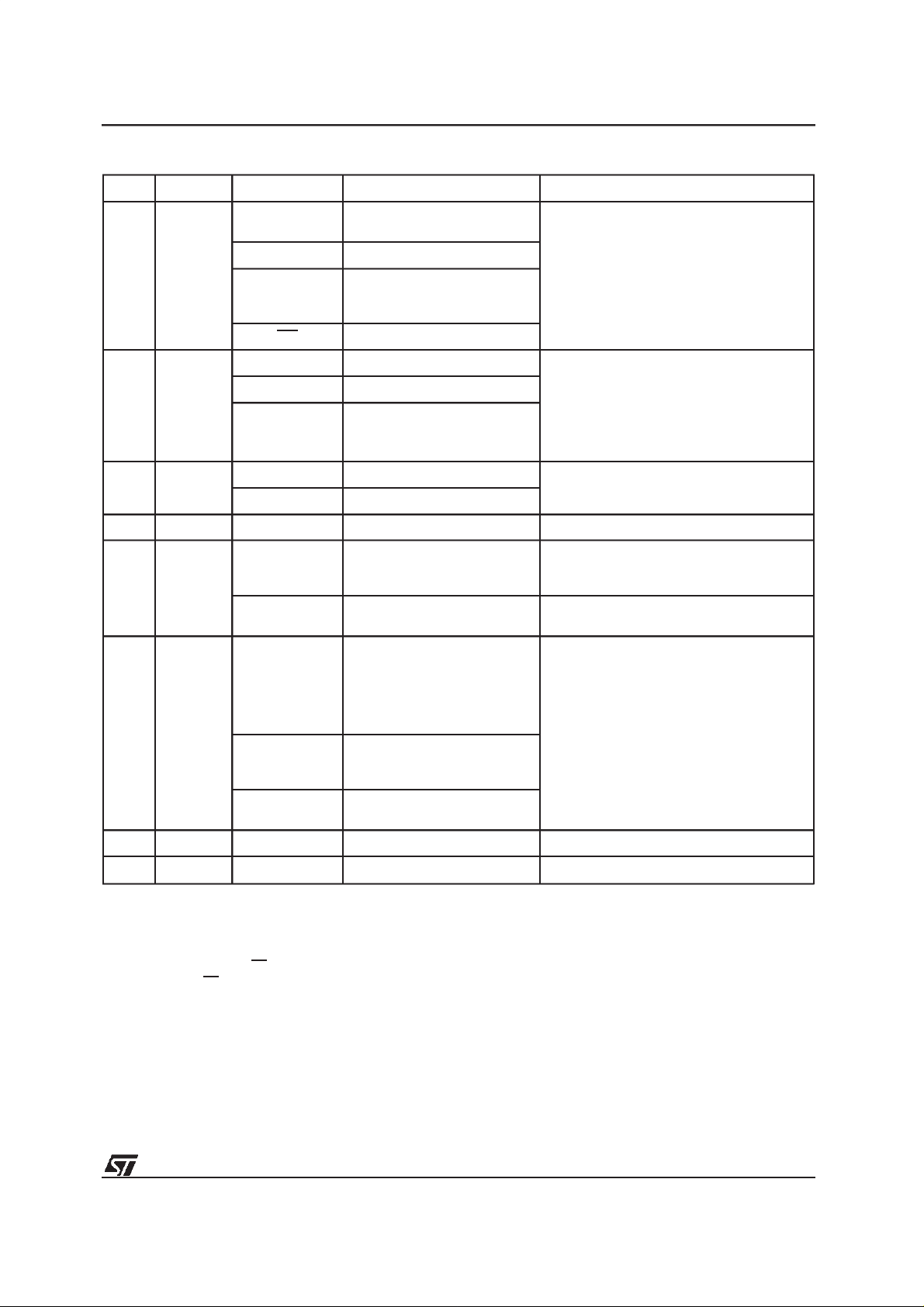
Table9. Status Register Bits
DQ Name Logic Level Definition Note
Erase Complete or erase
block in Erase Suspend
Program Complete or data
of non erase block during
Erase Suspend
Erase Complete or Erase
Suspend on currently
addressed block
Indicates theP/E.C. status, check during
Program or Erase,and on completion
before checkingbits DQ5 for Programor
Erase Success.
data onDQ6 whileProgramming or Erase
operations are on-going.DQ6 remains at
constant level when P/E.C. operations are
completed or EraseSuspend is
acknowledged.
Data
7
Polling
6 ToggleBit
’1’
’0’ Erase On-going
DQ
DQ Program On-going
’-1-0-1-0-1-0-1-’ Erase or Program On-going Successive reads outputcomplementary
DQ Program Complete
’-1-1-1-1-1-1-1-’
5 Error Bit
4 Reserved
Erase
3
TimeBit
2 ToggleBit
1 Reserved
0 Reserved
Notes: Logic level ’1’ is High, ’0’ is Low. -0-1-0-0-0-1-1-1-0- represent bit value in successive Readoperations.
’1’ Program or Erase Error
’0’ Program or Erase On-going
’1’ Erase TimeoutPeriod Expired
’0’
’-1-0-1-0-1-0-1-’
1
DQ
Erase Timeout Period
On-going
Chip Erase, Erase or Erase
Suspend on the currently
addressed block.
Erase Error due to the
currently addressed block
(when DQ5 = ’1’).
Program on-going, Erase
on-going on another block or
Erase Complete
Erase Suspend read on
non Erase Suspend block
This bit is setto ’1’in the case of
Programming orErase failure.
P/E.C. Erase operationhas started. Only
possible command entryis Erase
Suspend (ES).
An additional block to beerased in parallel
can beentered to the P/E.C.
Indicates theerase status and allows to
identify theerased block
that is after the fourthWpulseforprogrammingor
after the sixth W pulse for erase. It must be performed at the address being programmedor atan
address within the block being erased. If all the
blocksselectedforerasureare protected,DQ7will
be set to ’0’for about 100µs, andthenreturnto the
previous addressed memory data value. See Figure 11for the DataPollingflowchartandFigure 10
for the Data Polling waveforms.DQ7 will also flag
the Erase Suspend mode by switchingfrom ’0’ to
’1’ at the start of the Erase Suspend. In order to
monitor DQ7 in the Erase Suspend mode an address within a block being erased must be provided. For a Read Operation in Erase Suspend
mode, DQ7 will output ’1’ if the read is attempted
onablockbeingerasedandthedatavalueonother
blocks. During Program operation in Erase SuspendMode, DQ7 will have the same behaviouras
in the normal program execution outside of the
suspend mode.
11/34
 Loading...