

ST M29W320ET, M29W320EB User Manual
M29W320ET
M29W320EB
32 Mbit (4Mb x8 or 2Mb x16, Boot Block)
3V Supply Flash Memory
FEATURES SUMMARY
■SUPPLY VOLTAGE
–VCC = 2.7V to 3.6V for Program, Erase and Read
–VPP =12V for Fast Program (optional)
■ACCESS TIMES: 70, 90ns
■PROGRAMMING TIME
–10µs per Byte/Word typical
–Double Word/ Quadruple Byte Program
■MEMORY BLOCKS
–Memory Array: 63 Main Blocks
–8 Parameter Blocks (Top or Bottom Location)
■ERASE SUSPEND and RESUME MODES
–Read and Program another Block during Erase Suspend
■UNLOCK BYPASS PROGRAM COMMAND
–Faster Production/Batch Programming
■VPP/WP PIN for FAST PROGRAM and WRITE PROTECT
■TEMPORARY BLOCK UNPROTECTION MODE
■COMMON FLASH INTERFACE
–64 bit Security Code
■EXTENDED MEMORY BLOCK
–Extra block used as security block or to store additional information
■LOW POWER CONSUMPTION
–Standby and Automatic Standby
■100,000 PROGRAM/ERASE CYCLES per BLOCK
■ELECTRONIC SIGNATURE
–Manufacturer Code: 0020h
–Top Device Code M29W320ET: 2256h
–Bottom Device Code M29W320EB: 2257h
Figure 1. Packages
TSOP48 (N) 12 x 20mm
FBGA
TFBGA48 (ZE) 6 x 8mm
March 2005 |
1/46 |

M29W320ET, M29W320EB
TABLE OF CONTENTS
FEATURES SUMMARY . . . . . . . . . . . . . . . . . . . . . . . . . . . . . . . . . . . . . . . . . . . . . . . . . . . . . . . . . . . . . 1
Figure 1. Packages . . . . . . . . . . . . . . . . . . . . . . . . . . . . . . . . . . . . . . . . . . . . . . . . . . . . . . . . . . . . . . 1
SUMMARY DESCRIPTION . . . . . . . . . . . . . . . . . . . . . . . . . . . . . . . . . . . . . . . . . . . . . . . . . . . . . . . . . . . 5
Figure 2. Logic Diagram . . . . . . . . . . . . . . . . . . . . . . . . . . . . . . . . . . . . . . . . . . . . . . . . . . . . . . . . . . 5 Table 1. Signal Names . . . . . . . . . . . . . . . . . . . . . . . . . . . . . . . . . . . . . . . . . . . . . . . . . . . . . . . . . . 5 Figure 3. TSOP Connections . . . . . . . . . . . . . . . . . . . . . . . . . . . . . . . . . . . . . . . . . . . . . . . . . . . . . . 6 Figure 4. TFBGA48 Connections (Top view through package) . . . . . . . . . . . . . . . . . . . . . . . . . . . . 7 Figure 5. Block Addresses (x8). . . . . . . . . . . . . . . . . . . . . . . . . . . . . . . . . . . . . . . . . . . . . . . . . . . . . 8 Figure 6. Block Addresses (x16). . . . . . . . . . . . . . . . . . . . . . . . . . . . . . . . . . . . . . . . . . . . . . . . . . . . 9
SIGNAL DESCRIPTIONS . . . . . . . . . . . . . . . . . . . . . . . . . . . . . . . . . . . . . . . . . . . . . . . . . . . . . . . . . . . 10
Address Inputs (A0-A20). . . . . . . . . . . . . . . . . . . . . . . . . . . . . . . . . . . . . . . . . . . . . . . . . . . . . . . . . 10 Data Inputs/Outputs (DQ0-DQ7). . . . . . . . . . . . . . . . . . . . . . . . . . . . . . . . . . . . . . . . . . . . . . . . . . . 10 Data Inputs/Outputs (DQ8-DQ14). . . . . . . . . . . . . . . . . . . . . . . . . . . . . . . . . . . . . . . . . . . . . . . . . . 10 Data Input/Output or Address Input (DQ15A–1).. . . . . . . . . . . . . . . . . . . . . . . . . . . . . . . . . . . . . . . 10 Chip Enable (E). . . . . . . . . . . . . . . . . . . . . . . . . . . . . . . . . . . . . . . . . . . . . . . . . . . . . . . . . . . . . . . . 10 Output Enable (G). . . . . . . . . . . . . . . . . . . . . . . . . . . . . . . . . . . . . . . . . . . . . . . . . . . . . . . . . . . . . . 10 Write Enable (W). . . . . . . . . . . . . . . . . . . . . . . . . . . . . . . . . . . . . . . . . . . . . . . . . . . . . . . . . . . . . . . 10 VPP/Write Protect (VPP/WP). . . . . . . . . . . . . . . . . . . . . . . . . . . . . . . . . . . . . . . . . . . . . . . . . . . . . . . 10
Reset/Block Temporary Unprotect (RP). . . . . . . . . . . . . . . . . . . . . . . . . . . . . . . . . . . . . . . . . . . . . . 10 Ready/Busy Output (RB). . . . . . . . . . . . . . . . . . . . . . . . . . . . . . . . . . . . . . . . . . . . . . . . . . . . . . . . . 10 Byte/Word Organization Select (BYTE). . . . . . . . . . . . . . . . . . . . . . . . . . . . . . . . . . . . . . . . . . . . . . 11 VCC Supply Voltage (2.7V to 3.6V).. . . . . . . . . . . . . . . . . . . . . . . . . . . . . . . . . . . . . . . . . . . . . . . . . 11 VSS Ground. . . . . . . . . . . . . . . . . . . . . . . . . . . . . . . . . . . . . . . . . . . . . . . . . . . . . . . . . . . . . . . . . . . 11
BUS OPERATIONS. . . . . . . . . . . . . . . . . . . . . . . . . . . . . . . . . . . . . . . . . . . . . . . . . . . . . . . . . . . . . . . . 12
Bus Read. . . . . . . . . . . . . . . . . . . . . . . . . . . . . . . . . . . . . . . . . . . . . . . . . . . . . . . . . . . . . . . . . . . . . 12
Bus Write. . . . . . . . . . . . . . . . . . . . . . . . . . . . . . . . . . . . . . . . . . . . . . . . . . . . . . . . . . . . . . . . . . . . . 12
Output Disable. . . . . . . . . . . . . . . . . . . . . . . . . . . . . . . . . . . . . . . . . . . . . . . . . . . . . . . . . . . . . . . . . 12
Standby. . . . . . . . . . . . . . . . . . . . . . . . . . . . . . . . . . . . . . . . . . . . . . . . . . . . . . . . . . . . . . . . . . . . . . 12
Automatic Standby. . . . . . . . . . . . . . . . . . . . . . . . . . . . . . . . . . . . . . . . . . . . . . . . . . . . . . . . . . . . . . 12
Special Bus Operations . . . . . . . . . . . . . . . . . . . . . . . . . . . . . . . . . . . . . . . . . . . . . . . . . . . . . . . . 12
Electronic Signature. . . . . . . . . . . . . . . . . . . . . . . . . . . . . . . . . . . . . . . . . . . . . . . . . . . . . . . . . . . . . 12
Block Protect and Chip Unprotect. . . . . . . . . . . . . . . . . . . . . . . . . . . . . . . . . . . . . . . . . . . . . . . . . . 12
Table 2. Bus Operations, BYTE = VIL . . . . . . . . . . . . . . . . . . . . . . . . . . . . . . . . . . . . . . . . . . . . . . 13
Table 3. Bus Operations, BYTE = VIH . . . . . . . . . . . . . . . . . . . . . . . . . . . . . . . . . . . . . . . . . . . . . . 13
COMMAND INTERFACE . . . . . . . . . . . . . . . . . . . . . . . . . . . . . . . . . . . . . . . . . . . . . . . . . . . . . . . . . . . 14
Read/Reset Command . . . . . . . . . . . . . . . . . . . . . . . . . . . . . . . . . . . . . . . . . . . . . . . . . . . . . . . . . 14
Auto Select Command . . . . . . . . . . . . . . . . . . . . . . . . . . . . . . . . . . . . . . . . . . . . . . . . . . . . . . . . . 14
Read CFI Query Command . . . . . . . . . . . . . . . . . . . . . . . . . . . . . . . . . . . . . . . . . . . . . . . . . . . . . . 14
Program Command . . . . . . . . . . . . . . . . . . . . . . . . . . . . . . . . . . . . . . . . . . . . . . . . . . . . . . . . . . . . 14
2/46

M29W320ET, M29W320EB
Fast Program Commands . . . . . . . . . . . . . . . . . . . . . . . . . . . . . . . . . . . . . . . . . . . . . . . . . . . . . . . 15
Quadruple Byte Program Command. . . . . . . . . . . . . . . . . . . . . . . . . . . . . . . . . . . . . . . . . . . . . . . . 15
Double Word Program Command. . . . . . . . . . . . . . . . . . . . . . . . . . . . . . . . . . . . . . . . . . . . . . . . . . 15
Unlock Bypass Command . . . . . . . . . . . . . . . . . . . . . . . . . . . . . . . . . . . . . . . . . . . . . . . . . . . . . . 15
Unlock Bypass Program Command . . . . . . . . . . . . . . . . . . . . . . . . . . . . . . . . . . . . . . . . . . . . . . 15
Unlock Bypass Reset Command . . . . . . . . . . . . . . . . . . . . . . . . . . . . . . . . . . . . . . . . . . . . . . . . . 15
Chip Erase Command . . . . . . . . . . . . . . . . . . . . . . . . . . . . . . . . . . . . . . . . . . . . . . . . . . . . . . . . . . 15
Block Erase Command . . . . . . . . . . . . . . . . . . . . . . . . . . . . . . . . . . . . . . . . . . . . . . . . . . . . . . . . . 16
Erase Suspend Command . . . . . . . . . . . . . . . . . . . . . . . . . . . . . . . . . . . . . . . . . . . . . . . . . . . . . . 16
Erase Resume Command . . . . . . . . . . . . . . . . . . . . . . . . . . . . . . . . . . . . . . . . . . . . . . . . . . . . . . . 16
Enter Extended Block Command . . . . . . . . . . . . . . . . . . . . . . . . . . . . . . . . . . . . . . . . . . . . . . . . . 16
Exit Extended Block Command . . . . . . . . . . . . . . . . . . . . . . . . . . . . . . . . . . . . . . . . . . . . . . . . . . 17
Block Protect and Chip Unprotect Commands . . . . . . . . . . . . . . . . . . . . . . . . . . . . . . . . . . . . . 17
Table 4. Commands, 16-bit mode, BYTE = VIH. . . . . . . . . . . . . . . . . . . . . . . . . . . . . . . . . . . . . . . 17 Table 5. Commands, 8-bit mode, BYTE = VIL . . . . . . . . . . . . . . . . . . . . . . . . . . . . . . . . . . . . . . . . 18 Table 6. Program, Erase Times and Program, Erase Endurance Cycles . . . . . . . . . . . . . . . . . . . 18
STATUS REGISTER . . . . . . . . . . . . . . . . . . . . . . . . . . . . . . . . . . . . . . . . . . . . . . . . . . . . . . . . . . . . . . . 19
Data Polling Bit (DQ7). . . . . . . . . . . . . . . . . . . . . . . . . . . . . . . . . . . . . . . . . . . . . . . . . . . . . . . . . . . 19
Toggle Bit (DQ6).. . . . . . . . . . . . . . . . . . . . . . . . . . . . . . . . . . . . . . . . . . . . . . . . . . . . . . . . . . . . . . . 19
Error Bit (DQ5). . . . . . . . . . . . . . . . . . . . . . . . . . . . . . . . . . . . . . . . . . . . . . . . . . . . . . . . . . . . . . . . . 19
Erase Timer Bit (DQ3). . . . . . . . . . . . . . . . . . . . . . . . . . . . . . . . . . . . . . . . . . . . . . . . . . . . . . . . . . . 19
Alternative Toggle Bit (DQ2).. . . . . . . . . . . . . . . . . . . . . . . . . . . . . . . . . . . . . . . . . . . . . . . . . . . . . . 19
Table 7. Status Register Bits . . . . . . . . . . . . . . . . . . . . . . . . . . . . . . . . . . . . . . . . . . . . . . . . . . . . . 20
Figure 7. Data Polling Flowchart. . . . . . . . . . . . . . . . . . . . . . . . . . . . . . . . . . . . . . . . . . . . . . . . . . . 20
Figure 8. Toggle Flowchart . . . . . . . . . . . . . . . . . . . . . . . . . . . . . . . . . . . . . . . . . . . . . . . . . . . . . . . 20
MAXIMUM RATING. . . . . . . . . . . . . . . . . . . . . . . . . . . . . . . . . . . . . . . . . . . . . . . . . . . . . . . . . . . . . . . . 21
Table 8. Absolute Maximum Ratings . . . . . . . . . . . . . . . . . . . . . . . . . . . . . . . . . . . . . . . . . . . . . . . 21
DC and AC PARAMETERS . . . . . . . . . . . . . . . . . . . . . . . . . . . . . . . . . . . . . . . . . . . . . . . . . . . . . . . . . 22
Table 9. Operating and AC Measurement Conditions . . . . . . . . . . . . . . . . . . . . . . . . . . . . . . . . . . 22 Figure 9. AC Measurement I/O Waveform . . . . . . . . . . . . . . . . . . . . . . . . . . . . . . . . . . . . . . . . . . . 22 Figure 10.AC Measurement Load Circuit . . . . . . . . . . . . . . . . . . . . . . . . . . . . . . . . . . . . . . . . . . . . 22 Table 10. Device Capacitance. . . . . . . . . . . . . . . . . . . . . . . . . . . . . . . . . . . . . . . . . . . . . . . . . . . . . 22 Table 11. DC Characteristics. . . . . . . . . . . . . . . . . . . . . . . . . . . . . . . . . . . . . . . . . . . . . . . . . . . . . . 23 Figure 11.Read Mode AC Waveforms. . . . . . . . . . . . . . . . . . . . . . . . . . . . . . . . . . . . . . . . . . . . . . . 24 Table 12. Read AC Characteristics . . . . . . . . . . . . . . . . . . . . . . . . . . . . . . . . . . . . . . . . . . . . . . . . . 24 Figure 12.Write AC Waveforms, Write Enable Controlled . . . . . . . . . . . . . . . . . . . . . . . . . . . . . . . . 25 Table 13. Write AC Characteristics, Write Enable Controlled . . . . . . . . . . . . . . . . . . . . . . . . . . . . . 25 Figure 13.Write AC Waveforms, Chip Enable Controlled . . . . . . . . . . . . . . . . . . . . . . . . . . . . . . . . 26 Table 14. Write AC Characteristics, Chip Enable Controlled. . . . . . . . . . . . . . . . . . . . . . . . . . . . . . 26 Figure 14.Toggle and Alternative Toggle Bits Mechanism, Chip Enable Controlled . . . . . . . . . . . . 27 Figure 15.Toggle and Alternative Toggle Bits Mechanism, Output Enable Controlled . . . . . . . . . . 27 Table 15. Toggle and Alternative Toggle Bits AC Characteristics . . . . . . . . . . . . . . . . . . . . . . . . . . 27 Figure 16.Reset/Block Temporary Unprotect AC Waveforms . . . . . . . . . . . . . . . . . . . . . . . . . . . . . 28
3/46

M29W320ET, M29W320EB
Table 16. Reset/Block Temporary Unprotect AC Characteristics . . . . . . . . . . . . . . . . . . . . . . . . . . 28 Figure 17.Accelerated Program Timing Waveforms . . . . . . . . . . . . . . . . . . . . . . . . . . . . . . . . . . . . 28
PACKAGE MECHANICAL . . . . . . . . . . . . . . . . . . . . . . . . . . . . . . . . . . . . . . . . . . . . . . . . . . . . . . . . . . 29
Figure 18.TSOP48 Lead Plastic Thin Small Outline, 12x20 mm, Bottom View Package Outline . . 29 Table 17. TSOP48 Lead Plastic Thin Small Outline, 12x20 mm, Package Mechanical Data . . . . . 29 Figure 19.TFBGA48 6x8mm - 6x8 Ball Array, 0.8mm Pitch, Bottom View Package Outline. . . . . . 30 Table 18. TFBGA48 6x8mm - 6x8 Ball Array, 0.8mm Pitch, Package Mechanical Data. . . . . . . . . 30
PART NUMBERING . . . . . . . . . . . . . . . . . . . . . . . . . . . . . . . . . . . . . . . . . . . . . . . . . . . . . . . . . . . . . . . 31
Table 19. Ordering Information Scheme . . . . . . . . . . . . . . . . . . . . . . . . . . . . . . . . . . . . . . . . . . . . . 31
APPENDIX A.BLOCK ADDRESSES . . . . . . . . . . . . . . . . . . . . . . . . . . . . . . . . . . . . . . . . . . . . . . . . . . 32
Table 20. Top Boot Block Addresses, M29W320ET . . . . . . . . . . . . . . . . . . . . . . . . . . . . . . . . . . . . 32 Table 21. Bottom Boot Block Addresses, M29W320EB . . . . . . . . . . . . . . . . . . . . . . . . . . . . . . . . . 34
APPENDIX B.COMMON FLASH INTERFACE (CFI) . . . . . . . . . . . . . . . . . . . . . . . . . . . . . . . . . . . . . . 36
Table 22. Query Structure Overview . . . . . . . . . . . . . . . . . . . . . . . . . . . . . . . . . . . . . . . . . . . . . . . . 36 Table 23. CFI Query Identification String. . . . . . . . . . . . . . . . . . . . . . . . . . . . . . . . . . . . . . . . . . . . . 36 Table 24. CFI Query System Interface Information . . . . . . . . . . . . . . . . . . . . . . . . . . . . . . . . . . . . . 37 Table 25. Device Geometry Definition . . . . . . . . . . . . . . . . . . . . . . . . . . . . . . . . . . . . . . . . . . . . . . 37 Table 26. Primary Algorithm-Specific Extended Query Table . . . . . . . . . . . . . . . . . . . . . . . . . . . . . 38 Table 27. Security Code Area . . . . . . . . . . . . . . . . . . . . . . . . . . . . . . . . . . . . . . . . . . . . . . . . . . . . . 38
APPENDIX C.EXTENDED MEMORY BLOCK . . . . . . . . . . . . . . . . . . . . . . . . . . . . . . . . . . . . . . . . . . . 39
Factory Locked Extended Block . . . . . . . . . . . . . . . . . . . . . . . . . . . . . . . . . . . . . . . . . . . . . . . . . 39 Customer Lockable Extended Block . . . . . . . . . . . . . . . . . . . . . . . . . . . . . . . . . . . . . . . . . . . . . . 39
Table 28. Extended Block Address and Data . . . . . . . . . . . . . . . . . . . . . . . . . . . . . . . . . . . . . . . . . 39
APPENDIX D.BLOCK PROTECTION. . . . . . . . . . . . . . . . . . . . . . . . . . . . . . . . . . . . . . . . . . . . . . . . . . 40
Programmer Technique . . . . . . . . . . . . . . . . . . . . . . . . . . . . . . . . . . . . . . . . . . . . . . . . . . . . . . . . 40
In-System Technique . . . . . . . . . . . . . . . . . . . . . . . . . . . . . . . . . . . . . . . . . . . . . . . . . . . . . . . . . . 40
Table 29. Programmer Technique Bus Operations, BYTE = VIH or VIL . . . . . . . . . . . . . . . . . . . . . . . . . . . 40 Figure 20.Programmer Equipment Group Protect Flowchart . . . . . . . . . . . . . . . . . . . . . . . . . . . . . 41 Figure 21.Programmer Equipment Chip Unprotect Flowchart. . . . . . . . . . . . . . . . . . . . . . . . . . . . . 42 Figure 22.In-System Equipment Group Protect Flowchart . . . . . . . . . . . . . . . . . . . . . . . . . . . . . . . 43 Figure 23.In-System Equipment Chip Unprotect Flowchart . . . . . . . . . . . . . . . . . . . . . . . . . . . . . . 44
REVISION HISTORY . . . . . . . . . . . . . . . . . . . . . . . . . . . . . . . . . . . . . . . . . . . . . . . . . . . . . . . . . . . . . . . 45
Table 30. Document Revision History . . . . . . . . . . . . . . . . . . . . . . . . . . . . . . . . . . . . . . . . . . . . . . . 45
4/46
M29W320ET, M29W320EB
SUMMARY DESCRIPTION
The M29W320E is a 32 Mbit (4Mb x8 or 2Mb x16) non-volatile memory that can be read, erased and reprogrammed. These operations can be performed using a single low voltage (2.7 to 3.6V) supply. On power-up the memory defaults to its Read mode.
The device features an asymmetrical block architecture. The M29W320E has an array of 8 parameter and 63 main blocks. M29W320ET locates the Parameter Blocks at the top of the memory address space while the M29W320EB locates the Parameter Blocks starting from the bottom.
M29W320E has an extra 32 KWord (x16 mode) or 64 KByte (x8 mode) block, the Extended Block, that can be accessed using a dedicated command. The Extended Block can be protected and so is useful for storing security information. However the protection is irreversible, once protected the protection cannot be undone.
Each block can be erased independently so it is possible to preserve valid data while old data is
erased. The blocks can be protected to prevent accidental Program or Erase commands from modifying the memory. Program and Erase commands are written to the Command Interface of the memory. An on-chip Program/Erase Controller simplifies the process of programming or erasing the memory by taking care of all of the special operations that are required to update the memory contents. The end of a program or erase operation can be detected and any error conditions identified. The command set required to control the memory is consistent with JEDEC standards.
Chip Enable, Output Enable and Write Enable signals control the bus operation of the memory. They allow simple connection to most microprocessors, often without additional logic.
The memory is offered in TSOP48 (12x20mm), and TFBGA48 (6x8mm, 0.8mm pitch) packages. The memory is supplied with all the bits erased (set to ’1’).
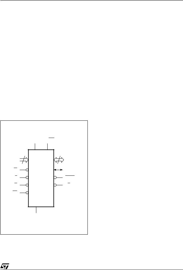
Figure 2. Logic Diagram
|
VCC VPP/WP |
|
|
21 |
|
15 |
|
A0-A20 |
|
DQ0-DQ14 |
|
W |
|
DQ15A–1 |
|
E |
M29W320ET |
BYTE |
|
M29W320EB |
|||
|
|
||
G |
|
RB |
|
RP |
|
|
VSS
AI09346
Table 1. Signal Names
|
A0-A20 |
Address Inputs |
|||||||||
|
|
|
|||||||||
|
DQ0-DQ7 |
Data Inputs/Outputs |
|||||||||
|
|
|
|||||||||
|
DQ8-DQ14 |
Data Inputs/Outputs |
|||||||||
|
|
|
|||||||||
|
DQ15A–1 |
Data Input/Output or Address Input |
|||||||||
|
|
|
|
|
|
|
|
|
|
|
|
|
|
|
|
|
|
|
|
|
|
|
Chip Enable |
|
E |
|
|
|
|
|
|
|
|
|
|
|
|
|
|
|
|
|
|
|
|
||
|
|
|
|
|
|
|
|
|
|
|
Output Enable |
|
G |
|
|
|
|
|
|
|
|||
|
|
|
|
|
|
|
|
|
|||
|
|
|
|
|
|
|
|
|
|
|
Write Enable |
|
W |
|
|
|
|
|
|
||||
|
|
|
|
|
|
|
|
||||
|
|
|
|
|
|
|
|
|
|
|
Reset/Block Temporary Unprotect |
|
RP |
|
|
|
|
|
|||||
|
|
|
|
|
|
||||||
|
|
|
|
|
|
|
|
|
|
|
Ready/Busy Output |
|
RB |
|
|
|
|
||||||
|
|
|
|
|
|||||||
|
|
|
|
|
|
|
|
|
|
|
Byte/Word Organization Select |
|
BYTE |
|
|
||||||||
|
|
|
|||||||||
|
VCC |
Supply Voltage |
|||||||||
|
VPP |
|
|
|
|
||||||
|
/WP |
|
VPP/Write Protect |
||||||||
|
VSS |
Ground |
|||||||||
|
NC |
Not Connected Internally |
|||||||||
|
|
|
|
|
|
|
|
|
|
|
|
5/46
M29W320ET, M29W320EB
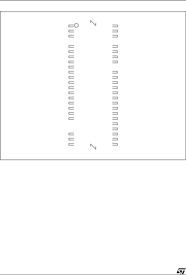
Figure 3. TSOP Connections
A15 |
1 |
|
|
48 |
|
|
A16 |
|||||||||||
A14 |
|
|
|
|
|
|
|
|
||||||||||
|
|
|
|
|
|
BYTE |
|
|||||||||||
A13 |
|
|
|
|
|
|
VSS |
|||||||||||
A12 |
|
|
|
|
|
|
|
DQ15A–1 |
||||||||||
|
|
|
|
|
|
|
||||||||||||
A11 |
|
|
|
|
|
|
DQ7 |
|||||||||||
A10 |
|
|
|
|
|
|
DQ14 |
|||||||||||
|
|
A9 |
|
|
|
|
|
|
DQ6 |
|||||||||
|
|
A8 |
|
|
|
|
|
|
DQ13 |
|||||||||
A19 |
|
M29W320ET |
|
|
DQ5 |
|||||||||||||
|
|
|
||||||||||||||||
A20 |
|
|
|
DQ12 |
||||||||||||||
|
M29W320EB |
|
|
|||||||||||||||
|
|
|
|
|
|
|
|
|
|
|
DQ4 |
|||||||
|
|
|
W |
|
|
|
|
|
|
|
||||||||
|
|
|
12 |
37 |
|
|
VCC |
|||||||||||
|
|
RP |
|
|
|
|||||||||||||
|
NC |
13 |
36 |
|
|
DQ11 |
||||||||||||
VPP |
|
|
|
|
|
|
|
|
DQ3 |
|||||||||
/WP |
|
|
|
|
|
|
||||||||||||
|
|
|
|
|
|
|
|
|
|
DQ10 |
||||||||
|
RB |
|
|
|
|
|
|
|
||||||||||
A18 |
|
|
|
|
|
|
DQ2 |
|||||||||||
A17 |
|
|
|
|
|
|
DQ9 |
|||||||||||
|
|
A7 |
|
|
|
|
|
|
DQ1 |
|||||||||
|
|
A6 |
|
|
|
|
|
|
DQ8 |
|||||||||
|
|
A5 |
|
|
|
|
|
|
|
DQ0 |
||||||||
|
|
|
|
|
|
|
||||||||||||
|
|
A4 |
|
|
|
|
|
|
|
|
|
|
|
|
||||
|
|
|
|
|
|
|
|
|
|
G |
|
|
||||||
|
|
|
|
|
|
|
|
|
|
|||||||||
|
|
A3 |
|
|
|
|
|
|
VSS |
|||||||||
|
|
A2 |
|
|
|
|
|
|
E |
|
||||||||
|
|
A1 |
24 |
|
|
25 |
|
|
A0 |
|||||||||
AI09347
6/46

M29W320ET, M29W320EB
Figure 4. TFBGA48 Connections (Top view through package)
|
1 |
2 |
3 |
4 |
5 |
6 |
A |
A3 |
A7 |
RB |
W |
A9 |
A13 |
B |
A4 |
A17 |
VPP/WP |
RP |
A8 |
A12 |
C |
A2 |
A6 |
A18 |
NC |
A10 |
A14 |
|
|
|
|
|
|
|
D |
A1 |
A5 |
A20 |
A19 |
A11 |
A15 |
E |
A0 |
DQ0 |
DQ2 |
DQ5 |
DQ7 |
A16 |
|
|
|
|
|
|
|
F |
E |
DQ8 |
DQ10 |
DQ12 |
DQ14 |
BYTE |
|
|
|
|
|
|
|
G |
G |
DQ9 |
DQ11 |
VCC |
DQ13 |
DQ15 |
A–1 |
||||||
H |
VSS |
DQ1 |
DQ3 |
DQ4 |
DQ6 |
VSS |
AI08084
7/46
M29W320ET, M29W320EB
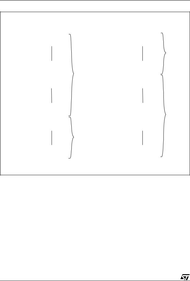
Figure 5. Block Addresses (x8)
|
Top Boot Block (x8) |
|
Bottom Boot Block (x8) |
|||
Address lines A20-A0, DQ15A-1 |
Address lines A20-A0, DQ15A-1 |
|||||
000000h |
|
|
000000h |
|
|
|
64 KByte or |
|
|
8 KByte or |
|
||
|
|
|
|
|
||
00FFFFh |
32 KWord |
|
001FFFh |
|
4 KWord |
|
|
|
|
|
|
||
Total of 8
Parameter
Blocks (1)
2F0000h |
64 KByte or |
|
00E000h |
8 KByte or |
|
|
|
||
2FFFFFh |
32 KWord |
Total of 63 |
00FFFFh |
4 KWord |
|
Main Blocks |
|
||
300000h |
|
010000h |
|
|
64 KByte or |
|
64 KByte or |
||
|
|
|
||
30FFFFh |
32 KWord |
|
01FFFFh |
32 KWord |
|
|
|
3E0000h |
|
64 KByte or |
|
0F0000h |
64 KByte or |
|
|
|
|
|
Total of 63 |
||
3EFFFFh |
|
32 KWord |
|
0FFFFFh |
32 KWord |
|
|
|
|
|
Main Blocks |
||
|
|
|
|
|||
3F0000h |
|
8 KByte or |
|
100000h |
64 KByte or |
|
|
|
|
|
|
||
3F1FFFh |
|
4 KWord |
|
10FFFFh |
32 KWord |
|
|
|
Total of 8 |
|
|
||
|
|
|
|
|
|
|
|
|
|
Parameter |
|
|
|
|
|
|
Blocks (1) |
|
|
|
3FE000h |
|
|
|
3F0000h |
|
|
|
8 KByte or |
|
64 KByte or |
|
||
|
|
|
|
|
||
3FFFFFh |
|
4 KWord |
|
3FFFFFh |
32 KWord |
|
|
|
|
|
|
||
Note 1. Used as Extended Block Addresses in Extended Block mode. |
|
|
AI09348 |
|||
Note: Also see APPENDIX A., Table 20. and Table 21. for a full listing of the Block Addresses.
8/46
|
|
|
|
|
|
M29W320ET, M29W320EB |
|
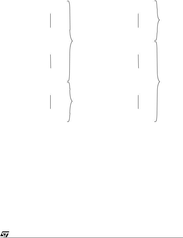
Figure 6. Block Addresses (x16) |
|
|
|
|
|
||
|
|
Top Boot Block (x16) |
|
|
Bottom Boot Block (x16) |
||
|
Address lines A20-A0 |
|
|
Address lines A20-A0 |
|||
000000h |
|
|
|
000000h |
|
|
|
|
64 KByte or |
|
|
8 KByte or |
|
||
|
|
|
|
|
|
||
007FFFh |
|
32 KWord |
|
000FFFh |
|
4 KWord |
|
|
|
|
|
|
Total of 8 |
||
|
|
|
|
|
|
|
|
|
|
|
|
|
|
|
Parameter |
|
|
|
|
|
|
|
Blocks (1) |
178000h |
|
|
|
007000h |
|
|
|
|
64 KByte or |
|
|
8 KByte or |
|
||
|
|
|
|
|
|
||
17FFFFh |
|
32 KWord |
Total of 63 |
007FFFh |
|
4 KWord |
|
|
|
|
|
|
|||
180000h |
|
|
Main Blocks |
008000h |
|
|
|
|
64 KByte or |
|
64 KByte or |
|
|||
|
|
|
|
|
|
||
187FFFh |
|
32 KWord |
|
00FFFFh |
|
32 KWord |
|
|
|
|
|
|
|
||
1F0000h |
|
|
|
078000h |
|
|
|
|
64 KByte or |
|
|
64 KByte or |
|
||
|
|
|
|
|
|
||
1F7FFFh |
|
32 KWord |
|
07FFFFh |
|
32 KWord |
Total of 63 |
|
|
|
|
|
|||
1F8000h |
|
|
|
080000h |
|
|
Main Blocks |
|
8 KByte or |
|
64 KByte or |
||||
|
|
|
|
|
|
||
1F8FFFh |
|
4 KWord |
|
087FFFh |
|
32 KWord |
|
|
|
Total of 8 |
|
|
|
||
|
|
|
|
|
|
|
|
|
|
|
Parameter |
|
|
|
|
|
|
|
Blocks (1) |
|
|
|
|
1FF000h |
|
|
|
1F8000h |
|
|
|
|
8 KByte or |
|
|
64 KByte or |
|
||
|
|
|
|
|
|
||
1FFFFFh |
|
4 KWord |
|
1FFFFFh |
|
32 KWord |
|
|
|
|
|
|
|
||
Note 1. Used as Extended Block Addresses in Extended Block mode. |
|
|
|
AI09349 |
|||
|
|
|
|
|
|
|
|
Note: Also see APPENDIX A., Table 20. and Table 21. for a full listing of the Block Addresses.
9/46

M29W320ET, M29W320EB
SIGNAL DESCRIPTIONS
See Figure 2., Logic Diagram, and Table 1., Signal Names, for a brief overview of the signals connected to this device.
Address Inputs (A0-A20). The Address Inputs select the cells in the memory array to access during Bus Read operations. During Bus Write operations they control the commands sent to the Command Interface of the Program/Erase Controller.
Data Inputs/Outputs (DQ0-DQ7). The Data I/O outputs the data stored at the selected address during a Bus Read operation. During Bus Write operations they represent the commands sent to the Command Interface of the Program/Erase Controller.
Data Inputs/Outputs (DQ8-DQ14). The Data I/O outputs the data stored at the selected address during a Bus Read operation when BYTE is High, VIH. When BYTE is Low, VIL, these pins are not used and are high impedance. During Bus Write operations the Command Register does not use these bits. When reading the Status Register these bits should be ignored.
Data Input/Output or Address Input (DQ15A–1).
When BYTE is High, VIH, this pin behaves as a Data Input/Output pin (as DQ8-DQ14). When BYTE is Low, VIL, this pin behaves as an address pin; DQ15A–1 Low will select the LSB of the addressed Word, DQ15A–1 High will select the MSB. Throughout the text consider references to the Data Input/Output to include this pin when BYTE is High and references to the Address Inputs to include this pin when BYTE is Low except when stated explicitly otherwise.
Chip Enable (E). The Chip Enable, E, activates the memory, allowing Bus Read and Bus Write operations to be performed. When Chip Enable is High, VIH, all other pins are ignored.
Output Enable (G). The Output Enable, G, controls the Bus Read operation of the memory.
Write Enable (W). The Write Enable, W, controls the Bus Write operation of the memory’s Command Interface.
VPP/Write Protect (VPP/WP). The VPP/Write Protect pin provides two functions. The VPP function allows the memory to use an external high voltage power supply to reduce the time required for Program operations. This is achieved by bypassing the unlock cycles and/or using the Double Word or Quadruple Byte Program commands.
The Write Protect function provides a hardware method of protecting the two outermost boot blocks. When VPP/Write Protect is Low, VIL, the memory protects the two outermost boot blocks; Program and Erase operations in these blocks are
10/46
ignored while VPP/Write Protect is Low, even when RP is at VID.
When VPP/Write Protect is High, VIH, the memory reverts to the previous protection status of the two outermost boot blocks. Program and Erase operations can now modify the data in these blocks unless the blocks are protected using Block Protection.
When VPP/Write Protect is raised to VPP the memory automatically enters the Unlock Bypass mode. When VPP/Write Protect returns to VIH or VIL normal operation resumes. During Unlock Bypass Program operations the memory draws IPP from the pin to supply the programming circuits. See the description of the Unlock Bypass command in the Command Interface section. The transitions from
VIH to VPP and from VPP to VIH must be slower than tVHVPP, see Figure 17.
Never raise VPP/Write Protect to VPP from any mode except Read mode, otherwise the memory may be left in an indeterminate state.
The VPP/Write Protect pin must not be left floating or unconnected or the device may become unreliable. A 0.1µF capacitor should be connected between the VPP/Write Protect pin and the VSS Ground pin to decouple the current surges from the power supply. The PCB track widths must be sufficient to carry the currents required during Unlock Bypass Program, IPP.
Reset/Block Temporary Unprotect (RP). The Reset/Block Temporary Unprotect pin can be used to apply a Hardware Reset to the memory or to temporarily unprotect all Blocks that have been protected.
Note that if VPP/WP is at VIL, then the two outermost boot blocks will remain protected even if RP is at VID.
A Hardware Reset is achieved by holding Reset/ Block Temporary Unprotect Low, VIL, for at least tPLPX. After Reset/Block Temporary Unprotect goes High, VIH, the memory will be ready for Bus Read and Bus Write operations after tPHEL or tRHEL, whichever occurs last. See the Ready/Busy Output section, Table 16. and Figure 16., Reset/ Block Temporary Unprotect AC Waveforms, for more details.
Holding RP at VID will temporarily unprotect the protected Blocks in the memory. Program and Erase operations on all blocks will be possible. The transition from VIH to VID must be slower than
tPHPHH.
Ready/Busy Output (RB). The Ready/Busy pin is an open-drain output that can be used to identify when the device is performing a Program or Erase operation. During Program or Erase operations
M29W320ET, M29W320EB
Ready/Busy is Low, VOL. Ready/Busy is high-im- pedance during Read mode, Auto Select mode and Erase Suspend mode.
After a Hardware Reset, Bus Read and Bus Write operations cannot begin until Ready/Busy becomes high-impedance. See Table 16. and Figure 16., Reset/Block Temporary Unprotect AC Waveforms.
The use of an open-drain output allows the Ready/ Busy pins from several memories to be connected to a single pull-up resistor. A Low will then indicate that one, or more, of the memories is busy.
Byte/Word Organization Select (BYTE). The Byte/Word Organization Select pin is used to switch between the x8 and x16 Bus modes of the memory. When Byte/Word Organization Select is Low, VIL, the memory is in x8 mode, when it is High, VIH, the memory is in x16 mode.
VCC Supply Voltage (2.7V to 3.6V). VCC provides the power supply for all operations (Read, Program and Erase).
The Command Interface is disabled when the VCC Supply Voltage is less than the Lockout Voltage, VLKO. This prevents Bus Write operations from accidentally damaging the data during power up, power down and power surges. If the Program/ Erase Controller is programming or erasing during this time then the operation aborts and the memory contents being altered will be invalid.
A 0.1µF capacitor should be connected between the VCC Supply Voltage pin and the VSS Ground pin to decouple the current surges from the power supply. The PCB track widths must be sufficient to carry the currents required during Program and Erase operations, ICC3.
VSS Ground. VSS is the reference for all voltage measurements. The device features two VSS pins which must be both connected to the system ground.
11/46

M29W320ET, M29W320EB
BUS OPERATIONS
There are five standard bus operations that control the device. These are Bus Read, Bus Write, Output Disable, Standby and Automatic Standby.
See Table 2. and Table 3., Bus Operations, for a summary. Typically glitches of less than 5ns on Chip Enable or Write Enable are ignored by the memory and do not affect bus operations.
Bus Read. Bus Read operations read from the memory cells, or specific registers in the Command Interface. A valid Bus Read operation involves setting the desired address on the Address Inputs, applying a Low signal, VIL, to Chip Enable and Output Enable and keeping Write Enable High, VIH. The Data Inputs/Outputs will output the value, see Figure 11., Read Mode AC Waveforms, and Table 12., Read AC Characteristics, for details of when the output becomes valid.
Bus Write. Bus Write operations write to the Command Interface. A valid Bus Write operation begins by setting the desired address on the Address Inputs. The Address Inputs are latched by the Command Interface on the falling edge of Chip Enable or Write Enable, whichever occurs last. The Data Inputs/Outputs are latched by the Command Interface on the rising edge of Chip Enable or Write Enable, whichever occurs first. Output Enable must remain High, VIH, during the whole Bus Write operation. See Figure 12. and Figure 13., Write AC Waveforms, and Table 13. and Table 14., Write AC Characteristics, for details of the timing requirements.
Output Disable. The Data Inputs/Outputs are in the high impedance state when Output Enable is High, VIH.
Standby. When Chip Enable is High, VIH, the memory enters Standby mode and the Data Inputs/Outputs pins are placed in the high-imped- ance state. To reduce the Supply Current to the Standby Supply Current, ICC2, Chip Enable should
be held within VCC ± 0.2V. For the Standby current level see Table 11., DC Characteristics.
During program or erase operations the memory will continue to use the Program/Erase Supply Current, ICC3, for Program or Erase operations until the operation completes.
Automatic Standby. If CMOS levels (VCC ± 0.2V) are used to drive the bus and the bus is inactive for 300ns or more the memory enters Automatic Standby where the internal Supply Current is reduced to the Standby Supply Current, ICC2. The Data Inputs/Outputs will still output data if a Bus Read operation is in progress.
Special Bus Operations
Additional bus operations can be performed to read the Electronic Signature and also to apply and remove Block Protection. These bus operations are intended for use by programming equipment and are not usually used in applications. They require VID to be applied to some pins.
Electronic Signature. The memory has two codes, the manufacturer code and the device code, that can be read to identify the memory. These codes can be read by applying the signals listed in Table 2. and Table 3., Bus Operations.
Block Protect and Chip Unprotect. Groups of blocks can be protected against accidental Program or Erase. The Protection Groups are shown in APPENDIX A., Table 20. and Table 21., Block Addresses. The whole chip can be unprotected to allow the data inside the blocks to be changed.
The VPP/Write Protect pin can be used to protect the two outermost boot blocks. When VPP/Write Protect is at VIL the two outermost boot blocks are protected and remain protected regardless of the Block Protection Status or the Reset/Block Temporary Unprotect pin status.
Block Protect and Chip Unprotect operations are described in APPENDIX D.
12/46

M29W320ET, M29W320EB
Table 2. Bus Operations, BYTE = VIL
|
|
|
|
|
|
|
|
|
|
|
Address Inputs |
|
Data Inputs/Outputs |
||
Operation |
|
E |
|
G |
|
W |
|
||||||||
|
|
|
|
|
|
||||||||||
|
|
|
|
DQ15A–1, A0-A20 |
DQ14-DQ8 |
DQ7-DQ0 |
|||||||||
|
|
|
|
|
|
|
|
|
|
|
|||||
|
|
|
|
|
|
|
|
|
|
|
|
|
|||
|
|
|
|
|
|
|
|||||||||
Bus Read |
VIL |
VIL |
VIH |
Cell Address |
Hi-Z |
Data Output |
|||||||||
Bus Write |
VIL |
VIH |
VIL |
Command Address |
Hi-Z |
Data Input |
|||||||||
Output Disable |
|
X |
VIH |
VIH |
X |
|
|
Hi-Z |
Hi-Z |
||||||
Standby |
VIH |
|
X |
|
X |
X |
|
|
Hi-Z |
Hi-Z |
|||||
Read Manufacturer |
VIL |
VIL |
VIH |
A0 |
= VIL, A1 = VIL, A9 = VID, |
Hi-Z |
20h |
||||||||
Code |
Others VIL or VIH |
||||||||||||||
|
|
|
|
|
|
|
|
|
|
|
|||||
Read Device Code |
VIL |
VIL |
VIH |
A0 |
= VIH, A1 = VIL, |
Hi-Z |
56h (M29W320ET) |
||||||||
A9 |
= VID, Others VIL or VIH |
57h (M29W320EB) |
|||||||||||||
|
|
|
|
|
|
|
|
|
|
|
|||||
Extended Memory |
VIL |
VIL |
VIH |
A0 |
= VIH, A1 = VIH, A6 = VIL, |
Hi-Z |
81h (factory locked) |
||||||||
Block Verify Code |
A9 |
= VID, Others VIL or VIH |
01h (not factory locked) |
||||||||||||
|
|
|
|
|
|
|
|
|
|
||||||
Note: X = VIL or VIH.
Table 3. Bus Operations, BYTE = VIH
|
|
|
|
|
|
|
|
|
|
|
Address Inputs |
Data Inputs/Outputs |
|
Operation |
|
E |
|
G |
|
W |
|
||||||
|
|
|
|
A0-A20 |
DQ15A–1, DQ14-DQ0 |
||||||||
|
|
|
|
|
|
|
|
|
|
|
|||
|
|
|
|
|
|
||||||||
Bus Read |
VIL |
VIL |
VIH |
Cell Address |
Data Output |
||||||||
|
|
|
|
|
|
||||||||
Bus Write |
VIL |
VIH |
VIL |
Command Address |
Data Input |
||||||||
Output Disable |
|
X |
VIH |
VIH |
X |
|
Hi-Z |
||||||
Standby |
VIH |
|
X |
|
X |
X |
|
Hi-Z |
|||||
Read Manufacturer |
VIL |
VIL |
VIH |
A0 |
= VIL, A1 = VIL, A9 = VID, |
0020h |
|||||||
Code |
Others VIL or VIH |
||||||||||||
|
|
|
|
|
|
|
|
|
|
||||
Read Device Code |
VIL |
VIL |
VIH |
A0 |
= VIH, A1 = VIL, A9 = VID, |
2256h (M29W320ET) |
|||||||
Others VIL or VIH |
2257h (M29W320EB) |
||||||||||||
|
|
|
|
|
|
|
|
|
|
||||
Extended Memory |
VIL |
VIL |
VIH |
A0 |
= VIH, A1 = VIH, A6 = VIL, |
81h (factory locked) |
|||||||
Block Verify Code |
A9 |
= VID, Others VIL or VIH |
01h (not factory locked) |
||||||||||
|
|
|
|
|
|
|
|
|
|||||
Note: X = VIL or VIH.
13/46

M29W320ET, M29W320EB
COMMAND INTERFACE
All Bus Write operations to the memory are interpreted by the Command Interface. Commands consist of one or more sequential Bus Write operations. Failure to observe a valid sequence of Bus Write operations will result in the memory returning to Read mode. The long command sequences are imposed to maximize data security.
The address used for the commands changes depending on whether the memory is in 16-bit or 8- bit mode. See either Table 4., or Table 5., depending on the configuration that is being used, for a summary of the commands.
Read/Reset Command
The Read/Reset command returns the memory to its Read mode. It also resets the errors in the Status Register. Either one or three Bus Write operations can be used to issue the Read/Reset command.
The Read/Reset command can be issued, between Bus Write cycles before the start of a program or erase operation, to return the device to read mode. If the Read/Reset command is issued during the time-out of a Block erase operation then the memory will take up to 10µs to abort. During the abort period no valid data can be read from the memory. The Read/Reset command will not abort an Erase operation when issued while in Erase Suspend.
Auto Select Command
The Auto Select command is used to read the Manufacturer Code, the Device Code, the Block Protection Status and the Extended Memory Block Verify Code. Three consecutive Bus Write operations are required to issue the Auto Select command. The memory remains in Auto Select mode until a Read/Reset or CFI Query command is issued.
In Auto Select mode the Manufacturer Code can be read using a Bus Read operation with A0 = VIL and A1 = VIL. The other address bits may be set to either VIL or VIH.
The Device Code can be read using a Bus Read operation with A0 = VIH and A1 = VIL. The other address bits may be set to either VIL or VIH.
The Block Protection Status of each block can be read using a Bus Read operation with A0 = VIL, A1 = VIH and A12-A20 specifying the block address. The other address bits may be set to either VIL or VIH. If the addressed block is protected then
01h is output on Data Inputs/Outputs DQ0-DQ7, otherwise 00h is output.
Read CFI Query Command
The Read CFI Query Command is used to read data from the Common Flash Interface (CFI) Memory Area. This command is valid when the device is in the Read Array mode, or when the device is in Auto Select mode.
One Bus Write cycle is required to issue the Read CFI Query Command. Once the command is issued subsequent Bus Read operations read from the Common Flash Interface Memory Area.
The Read/Reset command must be issued to return the device to the previous mode (the Read Array mode or Auto Select mode). A second Read/ Reset command would be needed if the device is to be put in the Read Array mode from Auto Select mode.
See APPENDIX B., Tables 22, 23, 24, 25, 26 and 27 for details on the information contained in the Common Flash Interface (CFI) memory area.
Program Command
The Program command can be used to program a value to one address in the memory array at a time. The command requires four Bus Write operations, the final write operation latches the address and data, and starts the Program/Erase Controller.
If the address falls in a protected block then the Program command is ignored, the data remains unchanged. The Status Register is never read and no error condition is given.
During the program operation the memory will ignore all commands. It is not possible to issue any command to abort or pause the operation. After programming has started, Bus Read operations output the Status Register content. See the section on the STATUS REGISTER for more details. Typical program times are given in Table 6.
After the program operation has completed the memory will return to the Read mode, unless an error has occurred. When an error occurs Bus Read operations will continue to output the Status Register. A Read/Reset command must be issued to reset the error condition and return to Read mode.
Note that the Program command cannot change a bit set at ’0’ back to ’1’. One of the Erase Commands must be used to set all the bits in a block or in the whole memory from ’0’ to ’1’.
14/46
 Loading...