

查询M29W320供应商
FEATURES SUMMARY
■ SUPPLY VOLTAGE
–V
–V
■ ACCESS TIME: 70, 90ns
■ PROGRAMMING TIME
– 10µs per Byte/Word typical
■ 67 MEMORY BLOCKS
– 1 Boot Block (Top or Bottom Location)
– 2 Parameter and 64 Main Blocks
■ PROGRAM/ERA SE CONTROLLER
– Embedded Byte/Word Program algorithms
■ ERASE SUSPEND and RESUME MODES
– Read and Program another Block during
■ UNLOCK BYPASS PROGRAM COMMAND
– Faster Production/Batch Progra mming
■ V
PP
PROTECT
■ TEMPORARY BLOCK UNPROTECTION
MODE
■ COMMON FLASH INTERFACE
– 64 bit Security Code
■ LOW POWER CONSUMPTION
– Standby and Automatic Standby
■ 100,000 PROGRAM/ERASE CYCL ES per
BLOCK
■ ELECTRONIC SIGNATURE
– Manufacturer Code: 0020h
– Top Device Code M29W320DT: 22CAh
– Bottom Device Code M29W320D B: 22CBh
2.7V to 3.6V for Program, Erase and
CC =
Read
=12V for Fast Program (optional)
PP
Erase Suspend
/WP PIN for F AST PROGRAM and WRIT E
M29W320DT
M29W320DB
32 Mbit (4Mb x8 or 2Mb x16, Boot Block)
3V Supp l y Fl ash Memory
Figure 1. Packages
TSOP48 (N)
12 x 20mm
FBGA
TFBGA63 (ZA)
TFBGA48 (ZE)
1/46August 2005

M29W320DT, M29W320DB
TABLE OF CONTENTS
FEATURES SUMMARY . . . . . . . . . . . . . . . . . . . . . . . . . . . . . . . . . . . . . . . . . . . . . . . . . . . . . . . . . . . . . 1
Figure 1. Packages. . . . . . . . . . . . . . . . . . . . . . . . . . . . . . . . . . . . . . . . . . . . . . . . . . . . . . . . . . . . . . 1
SUMMARY DESCRIPTION. . . . . . . . . . . . . . . . . . . . . . . . . . . . . . . . . . . . . . . . . . . . . . . . . . . . . . . . . . . 3
Figure 2. Logic Diagram . . . . . . . . . . . . . . . . . . . . . . . . . . . . . . . . . . . . . . . . . . . . . . . . . . . . . . . . . . 3
Table 1. Signal Names . . . . . . . . . . . . . . . . . . . . . . . . . . . . . . . . . . . . . . . . . . . . . . . . . . . . . . . . . . 3
Figure 3. TSOP Connections . . . . . . . . . . . . . . . . . . . . . . . . . . . . . . . . . . . . . . . . . . . . . . . . . . . . . .4
Figure 4. TFBGA63 Connections (Top view through package) . . . . . . . . . . . . . . . . . . . . . . . . . . . .5
Figure 5. TFBGA48 Connections (Top view through package) . . . . . . . . . . . . . . . . . . . . . . . . . . . .6
Figure 6. Block Addresses (x8). . . . . . . . . . . . . . . . . . . . . . . . . . . . . . . . . . . . . . . . . . . . . . . . . . . . . 7
Figure 7. Block Addresses (x16). . . . . . . . . . . . . . . . . . . . . . . . . . . . . . . . . . . . . . . . . . . . . . . . . . . . 8
SIGNAL DESCRIPTIONS . . . . . . . . . . . . . . . . . . . . . . . . . . . . . . . . . . . . . . . . . . . . . . . . . . . . . . . . . . . . 9
Address Inputs (A0-A20). . . . . . . . . . . . . . . . . . . . . . . . . . . . . . . . . . . . . . . . . . . . . . . . . . . . . . . . . . 9
Data Inputs/Outputs (DQ0-DQ7). . . . . . . . . . . . . . . . . . . . . . . . . . . . . . . . . . . . . . . . . . . . . . . . . . . . 9
Data Inputs/Outputs (DQ8-DQ14). . . . . . . . . . . . . . . . . . . . . . . . . . . . . . . . . . . . . . . . . . . . . . . . . . .9
Data Input/Output or Address Input (DQ15A–1).. . . . . . . . . . . . . . . . . . . . . . . . . . . . . . . . . . . . . . . . 9
Chip Enable (E
Output Enable (G
Write Enable (W
V
Write Protect (V
PP/
Reset/Block Temporary Unprotect (RP).. . . . . . . . . . . . . . . . . . . . . . . . . . . . . . . . . . . . . . . . . . . . . .9
Ready/Busy Output (RB
Byte/Word Organization Select (BYTE
V
Supply Voltage (2.7V to 3.6V).. . . . . . . . . . . . . . . . . . . . . . . . . . . . . . . . . . . . . . . . . . . . . . . . .10
CC
V
Ground. . . . . . . . . . . . . . . . . . . . . . . . . . . . . . . . . . . . . . . . . . . . . . . . . . . . . . . . . . . . . . . . . . . 10
SS
). . . . . . . . . . . . . . . . . . . . . . . . . . . . . . . . . . . . . . . . . . . . . . . . . . . . . . . . . . . . . . . . . 9
). . . . . . . . . . . . . . . . . . . . . . . . . . . . . . . . . . . . . . . . . . . . . . . . . . . . . . . . . . . . . . . 9
). . . . . . . . . . . . . . . . . . . . . . . . . . . . . . . . . . . . . . . . . . . . . . . . . . . . . . . . . . . . . . . .9
WP). . . . . . . . . . . . . . . . . . . . . . . . . . . . . . . . . . . . . . . . . . . . . . . . . . . . . . . . 9
PP/
). . . . . . . . . . . . . . . . . . . . . . . . . . . . . . . . . . . . . . . . . . . . . . . . . . . . . . . . . . 9
). . . . . . . . . . . . . . . . . . . . . . . . . . . . . . . . . . . . . . . . . . . . . . 10
BUS OPERATIONS. . . . . . . . . . . . . . . . . . . . . . . . . . . . . . . . . . . . . . . . . . . . . . . . . . . . . . . . . . . . . . . . 11
Bus Read. . . . . . . . . . . . . . . . . . . . . . . . . . . . . . . . . . . . . . . . . . . . . . . . . . . . . . . . . . . . . . . . . . . . . 11
Bus Write. . . . . . . . . . . . . . . . . . . . . . . . . . . . . . . . . . . . . . . . . . . . . . . . . . . . . . . . . . . . . . . . . . . . . 11
Output Disable. . . . . . . . . . . . . . . . . . . . . . . . . . . . . . . . . . . . . . . . . . . . . . . . . . . . . . . . . . . . . . . . . 11
Standby. . . . . . . . . . . . . . . . . . . . . . . . . . . . . . . . . . . . . . . . . . . . . . . . . . . . . . . . . . . . . . . . . . . . . . 11
Automatic Standby. . . . . . . . . . . . . . . . . . . . . . . . . . . . . . . . . . . . . . . . . . . . . . . . . . . . . . . . . . . . . . 11
Special Bus Operations . . . . . . . . . . . . . . . . . . . . . . . . . . . . . . . . . . . . . . . . . . . . . . . . . . . . . . . . 11
Electronic Signature. . . . . . . . . . . . . . . . . . . . . . . . . . . . . . . . . . . . . . . . . . . . . . . . . . . . . . . . . . . . . 11
Block Protect and Chip Unprotect. . . . . . . . . . . . . . . . . . . . . . . . . . . . . . . . . . . . . . . . . . . . . . . . . . 11
Figure 8. Bus Operations, BYTE
Table 2. Bus Operations, BYTE
= VIL . . . . . . . . . . . . . . . . . . . . . . . . . . . . . . . . . . . . . . . . . . . . . .11
= VIH. . . . . . . . . . . . . . . . . . . . . . . . . . . . . . . . . . . . . . . . . . . . . .12
COMMAND INTERFACE . . . . . . . . . . . . . . . . . . . . . . . . . . . . . . . . . . . . . . . . . . . . . . . . . . . . . . . . . . . 13
Read/Reset Command.. . . . . . . . . . . . . . . . . . . . . . . . . . . . . . . . . . . . . . . . . . . . . . . . . . . . . . . . . . 13
Auto Select Command. . . . . . . . . . . . . . . . . . . . . . . . . . . . . . . . . . . . . . . . . . . . . . . . . . . . . . . . . . . 13
Read CFI Query Command. . . . . . . . . . . . . . . . . . . . . . . . . . . . . . . . . . . . . . . . . . . . . . . . . . . . . . . 13
2/46

M29W320DT, M29W320DB
Program Command. . . . . . . . . . . . . . . . . . . . . . . . . . . . . . . . . . . . . . . . . . . . . . . . . . . . . . . . . . . . . 13
Unlock Bypass Command. . . . . . . . . . . . . . . . . . . . . . . . . . . . . . . . . . . . . . . . . . . . . . . . . . . . . . . . 13
Unlock Bypass Program Command.. . . . . . . . . . . . . . . . . . . . . . . . . . . . . . . . . . . . . . . . . . . . . . . . 14
Unlock Bypass Reset Command. . . . . . . . . . . . . . . . . . . . . . . . . . . . . . . . . . . . . . . . . . . . . . . . . . .14
Chip Erase Command. . . . . . . . . . . . . . . . . . . . . . . . . . . . . . . . . . . . . . . . . . . . . . . . . . . . . . . . . . . 1 4
Block Erase Command.. . . . . . . . . . . . . . . . . . . . . . . . . . . . . . . . . . . . . . . . . . . . . . . . . . . . . . . . . . 14
Erase Suspend Comma nd. . . . . . . . . . . . . . . . . . . . . . . . . . . . . . . . . . . . . . . . . . . . . . . . . . . . . . . . 14
Erase Resume Command. . . . . . . . . . . . . . . . . . . . . . . . . . . . . . . . . . . . . . . . . . . . . . . . . . . . . . . . 1 5
Block Protect and Chip Unprotect Commands.. . . . . . . . . . . . . . . . . . . . . . . . . . . . . . . . . . . . . . . . 15
Table 3. Com m ands , 16-bit mode, BYTE
Table 4. Com m ands , 8-bit mode, BYTE
Table 5. Program, Erase Times and Program, Erase Endurance Cycles . . . . . . . . . . . . . . . . . . . 18
STATUS REGISTER. . . . . . . . . . . . . . . . . . . . . . . . . . . . . . . . . . . . . . . . . . . . . . . . . . . . . . . . . . . . . . . 18
Data Polling Bit (DQ7). . . . . . . . . . . . . . . . . . . . . . . . . . . . . . . . . . . . . . . . . . . . . . . . . . . . . . . . . . . 18
Toggle Bit (DQ6).. . . . . . . . . . . . . . . . . . . . . . . . . . . . . . . . . . . . . . . . . . . . . . . . . . . . . . . . . . . . . . . 18
Error Bit (DQ5). . . . . . . . . . . . . . . . . . . . . . . . . . . . . . . . . . . . . . . . . . . . . . . . . . . . . . . . . . . . . . . . . 1 8
Erase Timer Bit (DQ3). . . . . . . . . . . . . . . . . . . . . . . . . . . . . . . . . . . . . . . . . . . . . . . . . . . . . . . . . . . 19
Alternative Toggle Bit (DQ2).. . . . . . . . . . . . . . . . . . . . . . . . . . . . . . . . . . . . . . . . . . . . . . . . . . . . . . 19
Table 6. Status Register Bits. . . . . . . . . . . . . . . . . . . . . . . . . . . . . . . . . . . . . . . . . . . . . . . . . . . . . 19
Figure 9. Data Polling Flowchart. . . . . . . . . . . . . . . . . . . . . . . . . . . . . . . . . . . . . . . . . . . . . . . . . . . 20
Figure 10.Data Toggle Flowchart . . . . . . . . . . . . . . . . . . . . . . . . . . . . . . . . . . . . . . . . . . . . . . . . . . 20
= VIH. . . . . . . . . . . . . . . . . . . . . . . . . . . . . . . . . . . . . . . 16
= VIL. . . . . . . . . . . . . . . . . . . . . . . . . . . . . . . . . . . . . . . . 17
MAXIMUM RATING. . . . . . . . . . . . . . . . . . . . . . . . . . . . . . . . . . . . . . . . . . . . . . . . . . . . . . . . . . . . . . . . 21
Table 7. Absolute Maximum Ratings. . . . . . . . . . . . . . . . . . . . . . . . . . . . . . . . . . . . . . . . . . . . . . . 21
DC and AC PARAMETERS . . . . . . . . . . . . . . . . . . . . . . . . . . . . . . . . . . . . . . . . . . . . . . . . . . . . . . . . . 22
Table 8. Operating and AC Measurement Conditions. . . . . . . . . . . . . . . . . . . . . . . . . . . . . . . . . . 22
Figure 11.AC Measurement I/O Waveform . . . . . . . . . . . . . . . . . . . . . . . . . . . . . . . . . . . . . . . . . . .22
Table 9. Dev ice Capacitanc e. . . . . . . . . . . . . . . . . . . . . . . . . . . . . . . . . . . . . . . . . . . . . . . . . . . . . 22
Table 10.DC Characteristics. . . . . . . . . . . . . . . . . . . . . . . . . . . . . . . . . . . . . . . . . . . . . . . . . . . . . . 23
Figure 13.Read Mode AC Waveforms . . . . . . . . . . . . . . . . . . . . . . . . . . . . . . . . . . . . . . . . . . . . . . . 24
Table 11.Read AC Characteristics . . . . . . . . . . . . . . . . . . . . . . . . . . . . . . . . . . . . . . . . . . . . . . . . .24
Figure 14.Write AC Waveforms, Write Enable Controlled. . . . . . . . . . . . . . . . . . . . . . . . . . . . . . . . 25
Table 12.Write AC Characteristics, Write Enable Controlled . . . . . . . . . . . . . . . . . . . . . . . . . . . . . 25
Figure 15.Write AC Waveforms, Chip Enable Controlled . . . . . . . . . . . . . . . . . . . . . . . . . . . . . . . . 26
Table 13. Write AC Characteristics, Chip Enable Controlled . . . . . . . . . . . . . . . . . . . . . . . . . . . . . .26
Figure 16.Reset/Block Temporary Unprotect AC Waveforms. . . . . . . . . . . . . . . . . . . . . . . . . . . . . 27
Table 14.Reset/Block Temporary Unprotect AC Characteristics . . . . . . . . . . . . . . . . . . . . . . . . . . 27
Figure 17.Accelerated Program Timing Waveforms . . . . . . . . . . . . . . . . . . . . . . . . . . . . . . . . . . . .27
PACKAGE MECHANICAL . . . . . . . . . . . . . . . . . . . . . . . . . . . . . . . . . . . . . . . . . . . . . . . . . . . . . . . . . . 2 8
Figure 18.TSOP48 Lead Plastic Thin Small Outline, 12x20 Mm, Bottom View Package Out line . . 28
Table 15. TSOP48 Lead Plastic Thin Small Outline, 12x20 mm, Package Mechani c al Data . . . . . 28
Figure 19.TFBGA63 7x11mm - 6x8 active ball array, 0.8mm pitch, Package Outline. . . . . . . . . . .29
Table 16. TF BGA 63 7x11mm - 6x8 active ball array, 0.8mm pitch, Package Mechanical Data . . . 29
3/46

M29W320DT, M29W320DB
Figure 20.TFBGA48 6x8mm - 6x8 Ball Array, 0.8mm Pitch, Bottom View Package Outline. . . . . . 30
Table 17. TF BGA 48 6x8m m - 6x8 Ball Array, 0.8mm Pitch, Package M echanical Data. . . . . . . . . 30
PART NUMBERING . . . . . . . . . . . . . . . . . . . . . . . . . . . . . . . . . . . . . . . . . . . . . . . . . . . . . . . . . . . . . . . 31
Table 18.Ordering Information Scheme . . . . . . . . . . . . . . . . . . . . . . . . . . . . . . . . . . . . . . . . . . . . . 31
APPENDIX A.BLOCK ADDRESS TABLE . . . . . . . . . . . . . . . . . . . . . . . . . . . . . . . . . . . . . . . . . . . . . .32
Table 19.Top Boot Block Addresses, M29W320DT. . . . . . . . . . . . . . . . . . . . . . . . . . . . . . . . . . . . 32
Table 20.Bottom Boot Block Addresses, M29W320DB . . . . . . . . . . . . . . . . . . . . . . . . . . . . . . . . .33
APPENDIX B.COMMON FLASH INTERFACE (CFI) . . . . . . . . . . . . . . . . . . . . . . . . . . . . . . . . . . . . . . 34
Table 21.Query Structure Overview . . . . . . . . . . . . . . . . . . . . . . . . . . . . . . . . . . . . . . . . . . . . . . . .34
Table 22.CFI Query Identification String. . . . . . . . . . . . . . . . . . . . . . . . . . . . . . . . . . . . . . . . . . . . .34
Table 23.CFI Query System Interface Information. . . . . . . . . . . . . . . . . . . . . . . . . . . . . . . . . . . . .35
Table 24. Device Geometry Definition . . . . . . . . . . . . . . . . . . . . . . . . . . . . . . . . . . . . . . . . . . . . . .35
Table 25. Prim ary Algorithm-Spec ific Extended Query Tabl e . . . . . . . . . . . . . . . . . . . . . . . . . . . . . 36
Table 26.Security Code Area . . . . . . . . . . . . . . . . . . . . . . . . . . . . . . . . . . . . . . . . . . . . . . . . . . . . . 37
APPENDIX C.BLOCK PROTECTION. . . . . . . . . . . . . . . . . . . . . . . . . . . . . . . . . . . . . . . . . . . . . . . . . . 38
Programmer Technique . . . . . . . . . . . . . . . . . . . . . . . . . . . . . . . . . . . . . . . . . . . . . . . . . . . . . . . . 3 8
In-System Technique . . . . . . . . . . . . . . . . . . . . . . . . . . . . . . . . . . . . . . . . . . . . . . . . . . . . . . . . . . 38
Table 27. Programmer Technique Bus Operations, BYTE
= VIH or V
IL . . . . . . . . . . . . . . . . . . . . . . . . . . . 38
Figure 21.Programmer Equipment Block Protect Flowchart . . . . . . . . . . . . . . . . . . . . . . . . . . . . . .39
Figure 22.Programmer Equipment Chip Unprotect Flowchart. . . . . . . . . . . . . . . . . . . . . . . . . . . . . 40
Figure 23.In-System Equipment Block Protect Flowchart . . . . . . . . . . . . . . . . . . . . . . . . . . . . . . . .41
Figure 24.In-System Equipment Chip Unprotect Flowchart . . . . . . . . . . . . . . . . . . . . . . . . . . . . . . 42
REVISION HISTORY . . . . . . . . . . . . . . . . . . . . . . . . . . . . . . . . . . . . . . . . . . . . . . . . . . . . . . . . . . . . . . . 43
Table 28.Document Revision History . . . . . . . . . . . . . . . . . . . . . . . . . . . . . . . . . . . . . . . . . . . . . . . 43
4/46
SUMMARY DESCRIPTION
The M29W320D is a 32 Mbit (4Mb x8 or 2Mb x16)
non-volatile memory that can be read, erased and
reprogrammed. These operations can be performed using a single low voltage (2.7 to 3.6V)
supply. On power-up the memory d efaults to its
Read mode where it can be read in the same way
as a ROM or EPROM.
The memory is divided into blocks that can be
erased independently so it is possible to pres erve
valid data while old data is erased. Each block can
be protected independently to prevent accidental
Program or Erase commands from modifying the
memory. Program and Erase c omm ands are wri tten to the Command Interface of t he memory. An
on-chip Program/Erase Controller simplifies the
process of programming or erasing the memory by
taking care of all of the special operations that are
required to update the memory contents. The end
of a program or erase op eration can be de tected
and any error conditions identified. The command
set required to control the memory is consistent
with JEDEC standards.
The blocks in the memory are as ymmetrically arranged, see Figure 6. and Figure 7., Table 19. and
Table 20.The first or l ast 6 4 Kby tes h ave been divided into four additional blocks. The 16 Kbyte
Boot Block can be used for small initialization code
to start the microprocessor, the two 8 Kbyte Parameter Blocks can be used for p aramet er storag e
and the remaining 32 K byte is a sm all Ma in Block
where the application may be stored.
Chip Enable, Output Enable and Write Enable signals control the bus operation of the memory.
They allow simple conne ction to most microprocessors, often without additional logic.
The memory is offered in TSOP48 (12 x 20mm)
TFBGA63 (7x11mm, 0.8mm pitch) and TFBGA48
(6x8mm, 0.8mm pitch) packages. The memory is
supplied with all the bi t s erased (set to 1 ).
M29W320DT, M29W320DB
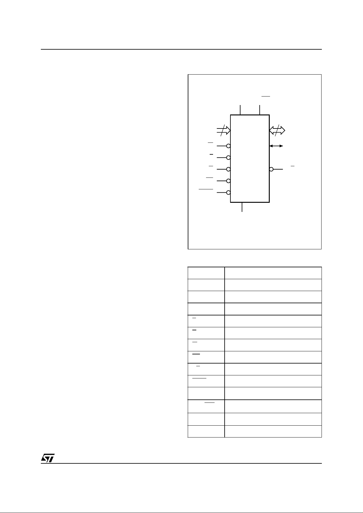
Figure 2. Logic Diagram
VPP/WP
V
CC
21
A0-A20
W
E
G
RP
BYTE
M29W320DT
M29W320DB
V
SS
Table 1. Signal Names
A0-A20 Address Inputs
DQ0-DQ7 Data Inputs/Outputs
DQ8-DQ14 Data Inputs/Outputs
DQ15A–1 Data Input/Output or Address Input
E
G
Chip Enable
Output Enable
15
DQ0-DQ14
DQ15A–1
RB
AI90189B
W
RP
RB
BYTE
V
CC
VPP/WP
V
SS
NC Not Connected Internally
Write Enable
Reset/Block Temporary Unprotect
Ready/Busy Output
Byte/Word Organization Select
Supply Voltage
VPP/Write Protect
Ground
5/46
M29W320DT, M29W320DB
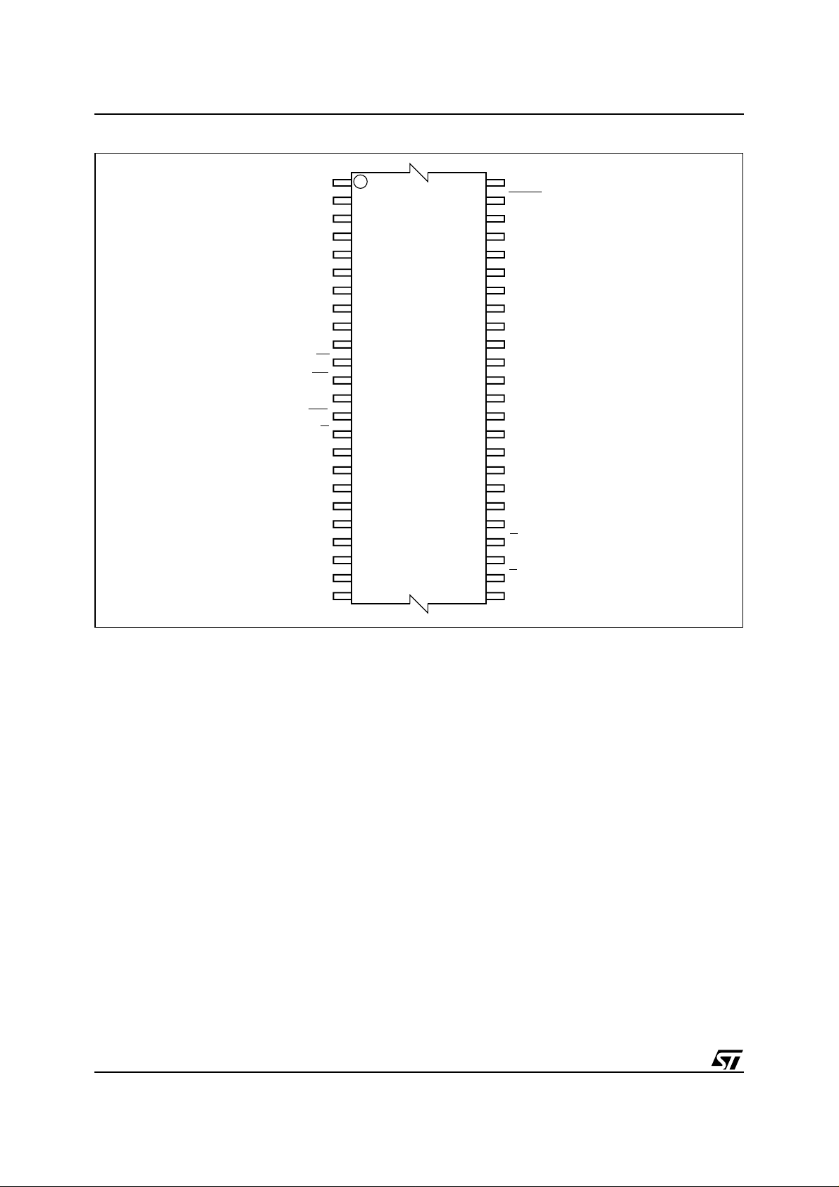
Figure 3. TSOP Connections
A15
1
48
A14
A13
A12
A11
A10 DQ14
A9
A8
A19
A20
W
RP
NC
12
M29W320DT
M29W320DB
13
37
36
VPP/WP
RB
A18
A17
A7
A6
A5
A4
A3
A2
A1
24 25
AI90190
A16
BYTE
V
SS
DQ15A–1
DQ7
DQ6
DQ13
DQ5
DQ12
DQ4
V
CC
DQ11
DQ3
DQ10
DQ2
DQ9
DQ1
DQ8
DQ0
G
V
SS
E
A0
6/46
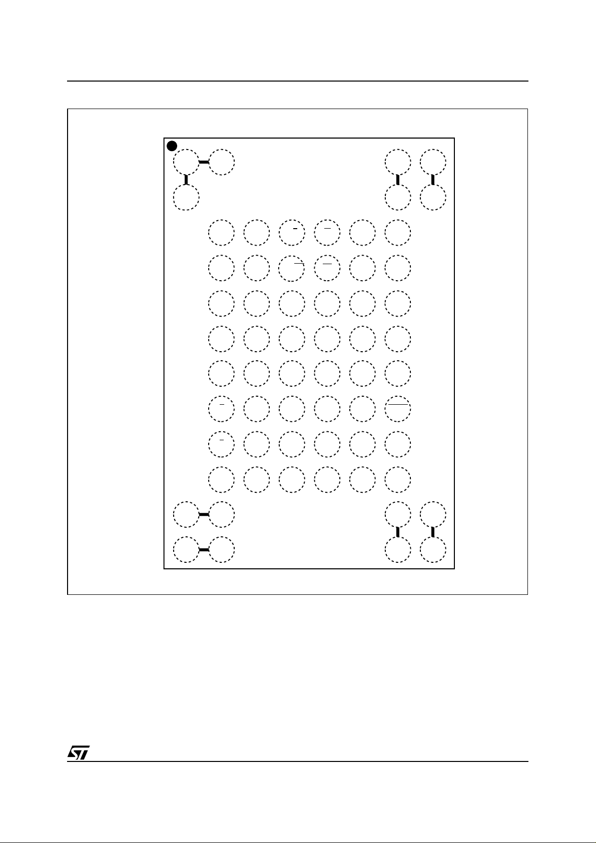
Figure 4. TFBGA63 Connections (Top view through packa ge)
M29W320DT, M29W320DB
654321
A
B
NC
NC
(1)
(1)
C
D
E
F
G
H
NC
A3
A4
A2
A1
A0
(1)
A7
A17
A6
RB
V
/
PP
A18
A5 A20
DQ0
E
DQ8
DQ2
DQ10
WP
W
RP
NC
A19
DQ5
DQ12
A9
A8
A10
A11
DQ7
DQ14
NC
NC
A13
A12
A14
A15
A16
BYTE
(1)
(1)
NC
NC
87
(1)
(1)
J
K
L
NC
M
NC
G
V
SS
(1)
NC
(1)
NC
DQ9
DQ1
(1)
(1)
DQ11
DQ3
V
CC
DQ4
Note: 1. Balls are shorted together via the substrate but not connected to the die.
DQ13
DQ6
DQ15
A–1
V
SS
NC
NC
NC
NC
(1)
(1)
AI05525B
(1)
(1)
7/46
M29W320DT, M29W320DB
Figure 5. TFBGA48 Connections (Top view through packa ge)
654321
A
B
C
D
E
F
G
H
A3
A4
A2
A1
A0
E
G
V
SS
A7
A17
A6
A5 A20
DQ0
DQ8
DQ9
DQ1
RB
V
PP
A18
DQ2
DQ10
DQ11
DQ3
/
WP
W
RP
NC
A19
DQ5
DQ12
V
CC
DQ4
A9
A8
A10
A11
DQ7
DQ14
DQ13
DQ6
A13
A12
A14
A15
A16
BYTE
DQ15
A–1
V
SS
AI08084
8/46
Figure 6. Block Addresses (x8)
M29W320DT, M29W320DB
M29W320DT
Top Boot Block Addresses (x8)
3FFFFFh
3FC000h
3FBFFFh
3FA000h
3F9FFFh
3F8000h
3F7FFFh
3F0000h
3EFFFFh
3E0000h
01FFFFh
010000h
00FFFFh
000000h
16 KByte
8 KByte
8 KByte
32 KByte
64 KByte
64 KByte
64 KByte
Total of 63
64 KByte Blocks
Bottom Boot Block Addresses (x8)
3FFFFFh
3F0000h
3EFFFFh
3E0000h
01FFFFh
010000h
00FFFFh
008000h
007FFFh
006000h
005FFFh
004000h
003FFFh
000000h
M29W320DB
64 KByte
64 KByte
64 KByte
32 KByte
8 KByte
8 KByte
16 KByte
Total of 63
64 KByte Blocks
Note: Also see APPEN DIX A., Table 19 . and Table 20. for a full listing of the Block Add res ses.
AI90192
9/46
M29W320DT, M29W320DB
Figure 7. Block Addresses (x16)
Top Boot Block Addresses (x16)
1FFFFFh
1FE000h
1FDFFFh
1FD000h
1FCFFFh
1FC000h
1FBFFFh
1F8000h
1F7FFFh
1F0000h
00FFFFh
008000h
007FFFh
000000h
M29W320DT
8 KWord
4 KWord
4 KWord
16 KWord
32 KWord
32 KWord
32 KWord
Total of 63
32 KWord Blocks
Bottom Boot Block Addresses (x16)
1FFFFFh
1F8000h
1F7FFFh
1F0000h
00FFFFh
008000h
007FFFh
004000h
003FFFh
003000h
002FFFh
002000h
001FFFh
000000h
M29W320DB
32 KWord
32 KWord
32 KWord
16 KWord
4 KWord
4 KWord
8 KWord
Total of 63
32 KWord Blocks
Note: Also see Appendix APPENDIX A., Table 19. and Table 20. for a full listing of the Block Addresses.
AI90193
10/46

SIGNAL DESCRIPTIONS
See Figure 2., Logic Diagram, and Table 1., Signal
Names, for a brief overview of the signals connected to this device.
Address Inputs (A0-A20). The Address Inputs
select the cell s in the memory arra y to access du ring Bus Read operations. During Bus Write operations they control the commands sent to the
Command Interface of the internal state machine.
Data Inputs/Outputs (DQ0-DQ7). The Data I/O
outputs the data stored at the selected address
during a Bus Read operation. During Bus Write
operations they represent the commands sent to
the Command Interface of the internal sta te machine.
Data Inputs/Outputs (DQ8-DQ14). The Data I/O
outputs the data stored at the selected address
during a Bus Read operation when B YTE
. When BYTE is Low, VIL, these pins are not
V
IH
is High,
used and are high impedance. During Bus Write
operations the Command Register does not use
these bits. When reading the Status Register
these bits should be ignored.
Data Input/Output o r Address Input (DQ15A –1).
When BYTE
is High, VIH, this pin behaves as a
Data Input/Output pin (as DQ8-DQ14). When
is Low, VIL, this pin behaves as an address
BYTE
pin; DQ15A–1 Low will select the LSB of the Word
on the other addresses, DQ15A–1 High will select
the MSB. Throughout the text consider references
to the Data Input/Output to include this pin when
is High and ref erences to the Address In-
BYTE
puts to include this pin when BYTE
is Low except
when stated explicitly otherwise.
Chip Enable (E
). The Chip Enable, E, activates
the memory, allowing Bus Read and Bus Write operations to be performed. When Chip Enable is
High, V
Output Enable (G
, all other pins are ignored.
IH
). The Output E nable, G, con-
trols the Bus Read operation of the memory.
Write Enable (W
). The Write Enable, W, controls
the Bus Write operation of the memory’s Command Interf a ce .
Write Protect (VPP/WP). The VPP/Write
V
PP/
Protect
pin provides two functions. The VPP function allo ws the memory to us e an external hi gh
volt age power s u pply to r educe th e time req ui red
for Unlock Bypass Program operations. The
Writ e Pro tec t fu nct io n prov i des a ha rd wa re me thod of protecting the 16 Kbyte Boot Block. The
/Write Protect pin must not be left floating or
V
PP
unconnected.
When V
/Write Protect is Low, VIL, the memo ry
PP
protects the 16 Kbyte Boot Block; Program and
Erase operations in this block are ignored while
/Write Protect is Low.
V
PP
M29W320DT, M29W320DB
When V
reverts to the previous protection status of the 16
Kbyte boot block. Program and Erase operations
can now modify the data in the 16 Kbyte Boot
Block unless the block is protected using Block
Protection.
When V
ory automatically enters the Unlock Bypass mode.
When V
mal operation resumes. During Unlock Bypass
Program operations the mem ory draws I
the pin to supply the programming circuits. See the
description of the Unlock Bypass c ommand in the
Command Interface section. The transitions from
to VPP and from VPP to VIH must be slower
V
IH
than t
Never raise V
mode except Read m ode, otherwise the memory
may be left in an indeterminate state.
A 0.1µF ca pacitor should be connected between
the V
to decouple the current surges from the power
supply. The PCB track widths must be sufficient to
carry the currents required during Unlock Bypass
Program, I
Reset/Block Temporary Unprotect (RP). The
Reset/Block Temporary Unprotect pin can be
used to apply a Hardware Reset to the memory or
to temporarily unprotect all Blocks that have b een
protected.
Note that if V
outermost boot block will remain protect even if RP
is at V
A Hardware Reset is achieved by holding Reset/
Block Temporary Unprotect Low, V
t
PLPX
goes High, V
Read and Bus Write operations after t
t
RHEL
Output section, Table 1 4. and Figure 16., Reset/
Temporary Unprotect AC Characteristics for more
details.
Holding RP
protected Blocks in the memory. Program and
Erase operations on all blocks will be possible.
The transition from V
t
PHPHH
Ready/Busy Output (RB
is an open-drain output that can be used to identify
when the device is performing a Program or Erase
operation. During Program or Erase operations
Ready/Busy is Low, V
pedance during Read mode, Auto Select mode
and Erase Suspend mode.
/Write Protect is High, VIH, the memory
PP
/Write Protect is raised to V
PP
/Write Protect returns to VIH or VIL nor-
PP
, see Figure 17..
VHVPP
/Write Protect to VPP from any
PP
/Write Protect pin and the VSS Ground pin
PP
.
PP
/WP is at VIL, then the 16 KByte
PP
.
ID
the mem-
PP
from
PP
, for at least
IL
. After Reset/Block Temporary Unprotect
, the memory will be ready for Bus
IH
PHEL
or
, whichever occurs last. See the Ready/Busy
at VID will temporarily unprotect the
to VID must be slower than
IH
.
). The Ready/Busy pin
. Ready/Busy is high-im-
OL
11/46

M29W320DT, M29W320DB
Note that if VPP/WP is at VIL, then the 16 KByte
outermost boot block will remain protect even if RP
is at V
ID
.
After a Hardware Reset, Bus Read and Bus Write
operations cannot begin until Ready/Busy becomes high-impedance. See Table 14. and Figure
Figure 16., Reset/Temporary Unprotect AC Characteristics.
The use of an open-drain output allows the Ready/
Busy pins from several memories to be connected
to a single pull-up resistor. A Low will then indicate
that one, or more, of the memories is busy.
Byte/Word Organization Select (BYTE
). The
Byte/Word Organization Select pin is used to
switch between the x8 and x16 Bus modes of the
memory. When Byte/Word Organization Select is
Low, V
High, V
, the memory is in x8 mode, when it is
IL
, the memory is in x16 mode.
IH
Supply Voltage (2.7V to 3.6V). VCC pro-
V
CC
vides the power supply for all operations (Read,
Program and Erase).
The Command Interface is disabled when the V
CC
Supply Voltage is less than the L ockout Voltage,
. This prevents Bus Write operations from ac-
V
LKO
cidentally damaging the data during power up,
power down and power surges. If the Program/
Erase Controller is programming or erasing during
this time then the operation aborts and the memory contents being altered will be invalid.
A 0.1µF ca pacitor should be connected between
the V
Supply Voltage pin and the VSS Ground
CC
pin to decouple the current surges from the power
supply. The PCB track widths must be sufficient to
carry the currents required during Program and
Erase operations, I
Ground. VSS is the reference for all voltage
V
SS
CC3
.
measurements.
12/46
BUS OPERATIONS
There are five standard bus operations that control
the device. These are Bus Read, Bus Write, Ou tput Disable, Standby and Automatic Standby. See
Figure 8. and Table 2., Bus Operations, for a summary. Typically glitches of less than 5ns on Chip
Enable or Write Enable are ignored by the memory
and do not affect bus operations.
Bus Read. Bus Read operations read from the
memory cells, or specific registers in the Command Interface. A valid Bus Read operation involves setting the desired address on the Address
Inputs, applying a Low sig nal, V
, to Chip Enable
IL
and Output Enable and keeping Write Enable
High, V
. The Data Inputs/Outputs will output the
IH
value, see Figure 13., Read Mode AC Waveforms,
and Table 11., Read AC Characteristics, for details of when the output becomes valid.
Bus Write. Bus Write operations write to the
Command Interface. A valid Bus Write operation
begins by setting the desire d address on t he Address Inputs. The Address Inputs are latc hed by
the Command Interface on the falling edge of Chip
Enable or Write Enable, whichever occurs last.
The Data Inputs/Outputs a re latched by the Command Interface on the rising edge of Chip Enable
or Write Enable, whichever occurs first. Output Enable must remain High, V
, during the whole Bus
IH
Write operation. See Figure 14. and Figure 15.,
Write AC Waveforms, and Table 12. and Table
13., Write AC Characteristics, for details of the timing requirements.
Output Disa bl e . T he Data Inputs/Outputs are in
the high impedance s tate when Output Enable is
High, V
Standby. When Chip Enable is High, V
.
IH
, the
IH
memory enters Standby mode and the Data In-
M29W320DT, M29W320DB
puts/Outputs pins are placed in the high-impedance state. To reduce t he Supply Current to the
Standby Supply Current, I
be held within V
± 0.2V. For the Standby current
CC
level see Table 10., DC Characteristics.
During program or erase operations the memory
will continue to use the Program/Erase Supply
Current, I
, for Program or Erase operations un-
CC3
til the operation completes.
Automatic Standby. If CMOS levels (V
are used to drive the bus and the bus is inactive for
300ns or more the memory enters Automatic
Standby where the internal Supply Current is reduced to the Standby Supply Current, I
Data Inputs/Outputs will still output data if a Bus
Read operation is in progress.
Special Bus Operations
Additional bus operations can be performed to
read the Electronic Signature and also to apply
and remove Block Protection. These bus operations are intended for use by programming equipment and are not usually used in applications.
They require V
to be applied to some pins.
ID
Electronic Signature. The memory has two
codes, the manufacturer code and the device
code, that can be read to identify the memory.
These codes can be read by applying t he signals
listed in Figure 8. and Table 2., Bus Operations.
Block Protect and Chip Unprotect.
can be separately protected against accidental
Program or Erase. T he whole chip can be unprotected to allow the data inside the blocks to be
changed.
Block Protect and Chip Unprote ct operations are
described in APPENDIX C..
, Chip Enable should
CC2
CC
CC2
Each block
± 0.2V)
. The
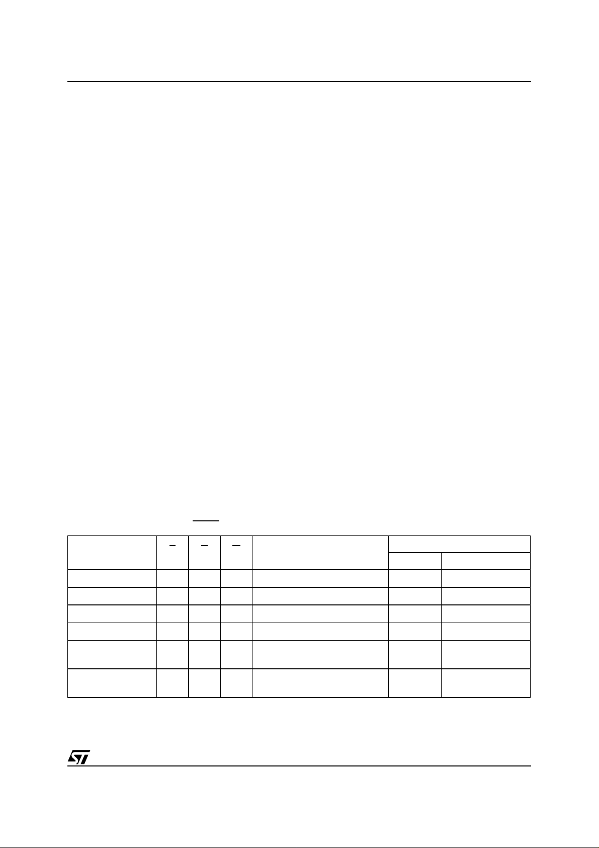
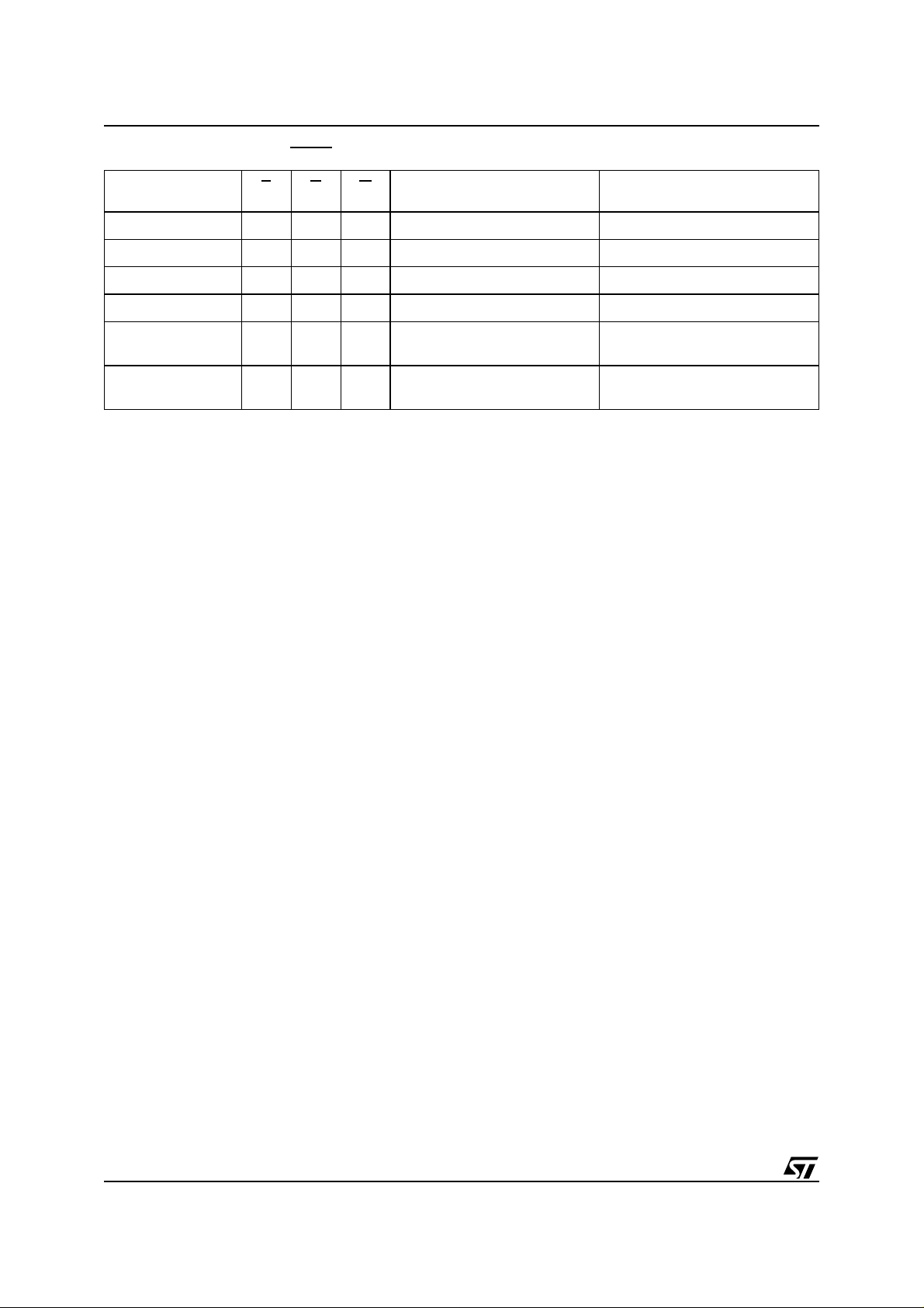
Figure 8. Bus Operations, BYTE
Operation E G W
Bus Read
Bus Write
Output Disable X
Standby
Read Manufacturer
Code
Read Device Code
Note: X = VIL or VIH.
V
V
V
V
V
V
IL
IL
IH
IL
IL
IL
V
IH
V
IH
X X X Hi-Z Hi-Z
V
IL
V
IL
= V
IL
Address Inputs
DQ15A–1, A0-A20
V
Cell Address Hi-Z Data Output
IH
V
Command Address Hi-Z Data Input
IL
V
X Hi-Z Hi-Z
IH
A0 = VIL, A1 = VIL, A9 = VID,
V
IH
Others VIL or V
A0 = VIH, A1 = VIL,
V
IH
A9 = VID, Others VIL or V
IH
IH
Data Inputs/Outputs
DQ14-DQ8 DQ7-DQ0
Hi-Z 20h
Hi-Z
CAh (M29W320DT)
CBh (M29W320DB)
13/46
M29W320DT, M29W320DB
Table 2. Bus Operations, BYTE = V
Operation E G W
Bus Read
Bus Write
Output Disable X
Standby
Read Manufacturer
Code
Read Device Code
Note: X = VIL or VIH.
V
V
V
V
V
V
IL
IL
IH
IL
IL
IL
V
IH
V
IH
XXX Hi-Z
V
IL
V
IL
IH
Address Inputs
A0-A20
V
Cell Address Data Output
IH
V
Command Address Data Input
IL
V
XHi-Z
IH
A0 = VIL, A1 = VIL, A9 = VID,
V
IH
Others V
A0 = VIH, A1 = VIL, A9 = VID,
V
IH
Others VIL or V
or V
IL
IH
IH
Data Inputs/Outputs
DQ15A–1, DQ14-DQ0
0020h
22CAh (M29W320DT)
22CBh (M29W320DB)
14/46
 Loading...