

2 Mbit (256Kb x8 or 128Kb x16, Boot Block)
Low Voltage Single Supply Flash Memory
■ SINGLE 2.7 to 3.6V SUPPLY VOLTAGE for
PROGRAM, ERASE and READ OPE RATI ONS
■ ACCESS TIME: 55ns
■ PROGRAMMING TIME
– 10µs per Byte/Word typical
■ 7 MEMORY BLOCKS
– 1 Boot Block (Top or Bottom Location)
– 2 Parameter and 4 Main Bl ocks
■ PROGRAM/ERASE CONTROLLER
– Embedded Byte/Word Program algorithm
– Embedded Multi-Block/Chip Erase algorithm
– Status Register Polling and Toggle Bits
– Ready/Busy Output Pin
■ ERASE SUSPEND and RESUME MODES
– Read and Program another Block during
Erase Suspend
■ UNLOCK BYPASS PROGRAM COMMAND
– Faster Production/Batch Programming
■ TEMPORARY BLOCK UNPROTECTION
MODE
■ LOW POWER CONSUMPTION
– Standby and Automatic Standby
■ 100,000 PROGRAM/ERASE CYCLES per
BLOCK
■ 20 YEARS DATA RETENTION
– Defectivity below 1 ppm/year
■ ELECTRONIC SIGNATURE
– Manufacturer Code : 0020h
– Top Device Code M29W200BT: 0051h
– Bottom Device Code: M29W200BB 0057h
■ ECOPACK
®
PACKAGES AVAILABLE
M29W200BT
M29W200BB
TSOP48 (N)
12 x 20mm
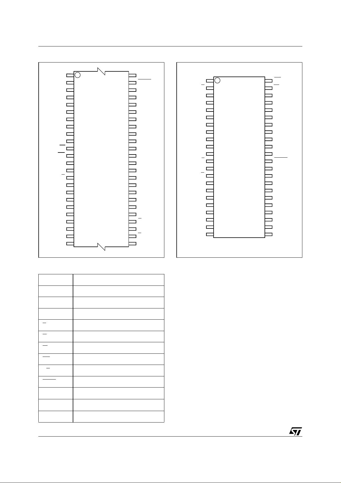
Figure 1. Logic Diagram
V
CC
17
A0-A16
W
E
G
RP
M29W200BT
M29W200BB
44
1
SO44 (M)
15
DQ0-DQ14
DQ15A–1
BYTE
RB
V
SS
AI02948
1/22September 2005
M29W200BT, M29W200BB
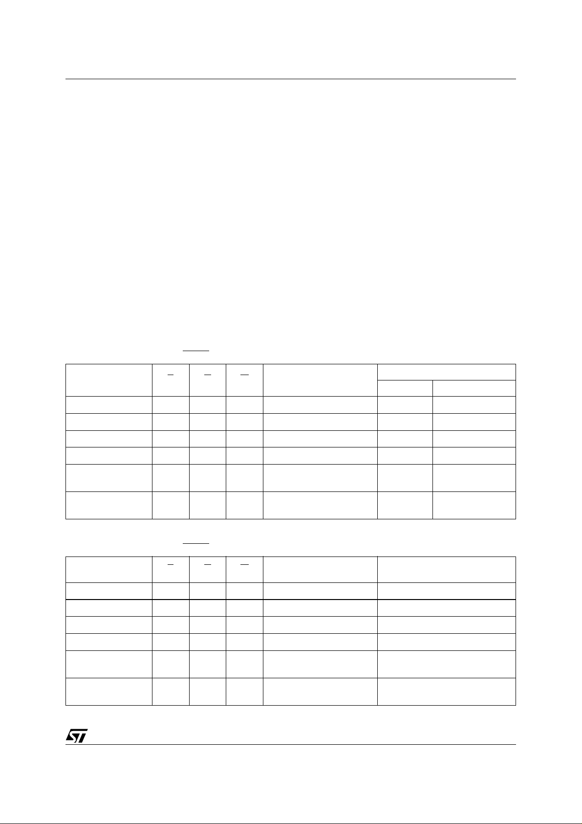
Figure 2. TSOP Connections
A15
A14
A13
A12
A11
A10 DQ14
A9
A8
NC
NC
RP
NC
NC
RB
NC
NC
A7
A6
A5
A4
A3
A2
A1
1
W
12
M29W200BT
M29W200BB
13
24 25
48
37
36
AI02944
A16
BYTE
V
SS
DQ15A–1
DQ7
DQ6
DQ13
DQ5
DQ12
DQ4
V
CC
DQ11
DQ3
DQ10
DQ2
DQ9
DQ1
DQ8
DQ0
G
V
SS
E
A0
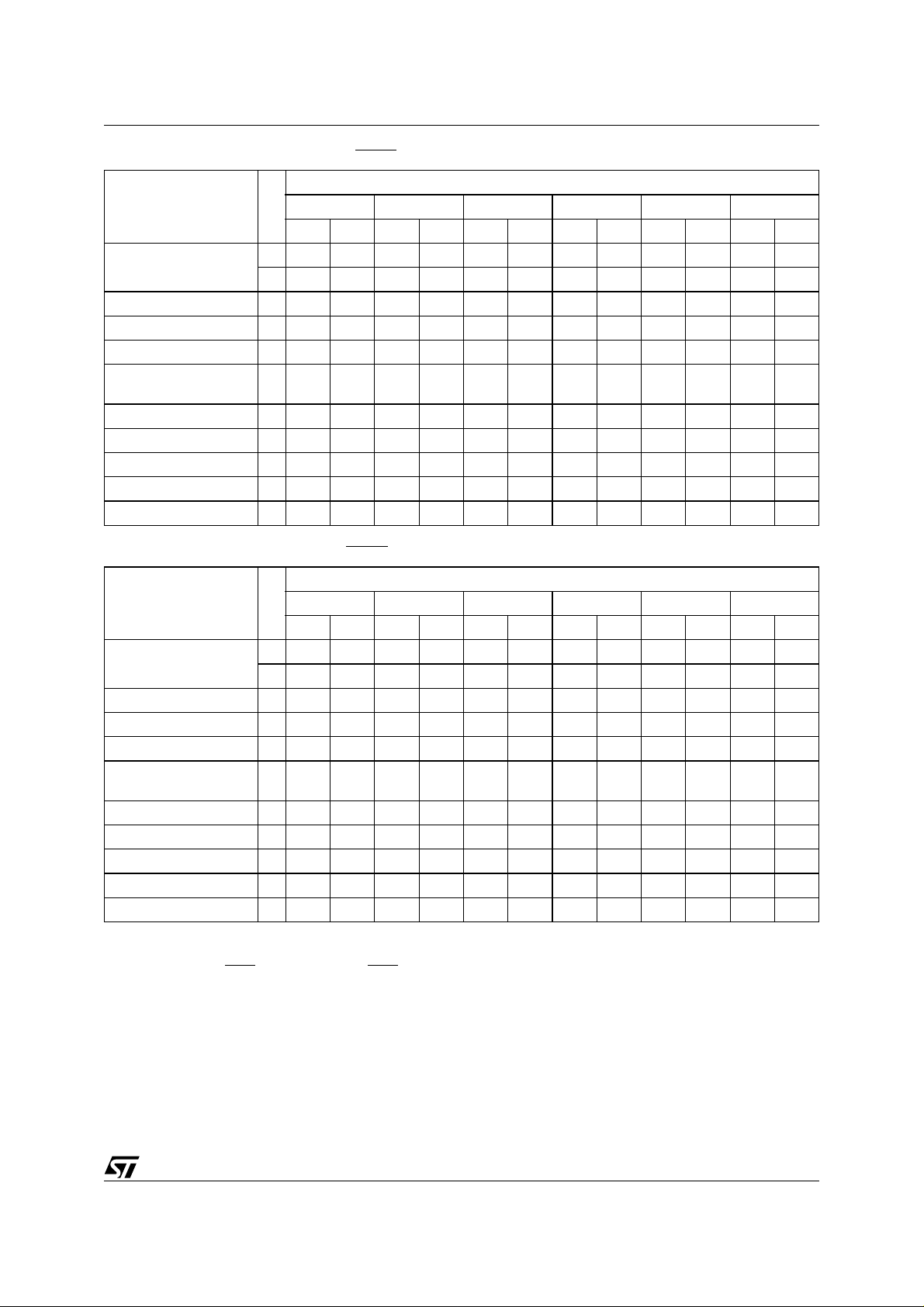
Figure 3. SO Connections
NC RP
NC A8
A7
A6
A5
A4
A3
A2
A1
A0
V
SS
DQ0
DQ8
DQ9
DQ10
DQ3
DQ11
1
2
3
4
5
6
7
8
9
10
11
M29W200BT
E
G
M29W200BB
12
13
14
15
16
17DQ1
18
19
20
21
44
43
42
41
40
39
38
37
36
35
34
33
32
31
30
29
28
27
26
25
24
2322
AI02945
WRB
A9
A10
A11
A12
A13
A14
A15
A16
BYTE
V
SS
DQ15A–1
DQ7
DQ14
DQ6
DQ13
DQ5DQ2
DQ12
DQ4
V
CC
Table 1. Signal Names
A0-A16 Address Inputs
DQ0-DQ7 Data Inputs/Outputs
DQ8-DQ14 Data Inputs/Outputs
DQ15A–1 Data Input/Output or Address Input
E
G
W
RP
RB
BYTE
V
CC
V
SS
NC Not Connected Internally
2/22
Chip Enable
Output Enable
Write Enable
Reset/Block Temporary Unprotect
Ready/Busy Output
Byte/Word Organization Select
Supply Voltage
Ground
SUMMARY DESCRIPTION
The M29W200B is a 2 M bit (256Kb x8 or 128Kb
x16) non-volatile memory that can be read, erased
and reprogrammed. These operations can be performed using a single low voltage (2.7 to 3.6V)
supply. On power-up the memory defaults to its
Read mode where it can be read in the same way
as a ROM or EPROM. The M29W200B is fully
backward compatible with the M29W200.
The memory is divided into blocks that can be
erased independently s o i t is po ss ible to preserve
valid data while old data is erased. Each block can
be protected independen tly to prevent accidental
Program or Erase com mands from modifying the
memory. Program and Erase co mmands are written to the Command Int erface of th e memory . An
on-chip Program/Erase Controller simplifies the
process of programming or erasing the memory by
taking care of all of the special operations that are
required to update the memory contents. The end
of a program or erase operation ca n be detected
and any error conditions ide nti fie d. T he co mma nd
set required to control the memory is consistent
with JEDEC standards.

M29W200BT, M29W200BB
Table 2. Absolute Maximum Ratings
Symbol Parameter Value Unit
T
A
T
BIAS
T
STG
(2)
V
IO
V
CC
V
ID
Note: 1. Except for the rating "Operating Temperature Range", stresses above those listed in the Table "Absolute Maximum Ratings" may
cause permanent damage to the device. Thes e are str ess ratin gs only and oper at ion of the device at thes e or any ot her condi tio ns
above those indicated in the Operating sections of this specification is not implied. Exposure to Absolute Maximum Rating conditions for extended periods may affect dev ice reliability. Refer also to the S TMicroelectronics SURE Progr am and other relevant quality documents.
2. Minimum Voltage may undershoot to –2V during transition and for less than 20ns during transitions.
Ambient Operating Temperature (Temperature Range Option 1) 0 to 70 °C
Ambient Operating Temperature (Temperature Range Option 6) –40 to 85 °C
Temperature Under Bias –50 to 125 °C
Storage Temperature –65 to 150 °C
Input or Output Voltage –0.6 to 4 V
Supply Voltage –0.6 to 4 V
Identification Voltage –0.6 to 13.5 V
Table 3. Top Boot Block Addresses M29W200BT
Size
#
(Kbytes)
6 16 3C000h-3FFFFh 1E000h-1FFFFh
5 8 3A000h-3BFFFh 1D000h-1DFFFh
4 8 38000h-39FFFh 1C000h-1CFFFh
3 32 30000h-37FFFh 18000h-1BFFFh
2 64 20000h-2FFFFh 10000h-17FFFh
1 64 10000h-1FFFFh 08000h-0FFFFh
0 64 00000h-0FFFFh 00000h-07FFFh
Address Range
(x8)
(1)
Address Range
(x16)
Table 4. Bottom Boot Block Addresses M29W200BB
Size
#
(Kbytes)
6 64 30000h-3FFFFh 18000h-1FFFFh
5 64 20000h-2FFFFh 10000h-17FFFh
4 64 10000h-1FFFFh 08000h-0FFFFh
3 32 08000h-0FFFFh 04000h-07FFFh
2 8 06000h-07FFFh 03000h-03FFFh
1 8 04000h-05FFFh 02000h-02FFFh
0 16 00000h-03FFFh 00000h-01FFFh
Address Range
(x8)
Address Range
(x16)
The blocks in the memo ry are asymmet rically arranged, see Tables 3 and 4, Block Addresses. The
first or last 64 Kbytes have been divided into fou r
additional blocks. The 16 Kbyte Boot Block can be
used for small initialization code to start the microprocessor, the two 8 Kby te Parameter Blocks can
be used for parameter s torage and the remaining
32K is a small Ma in Block where the applicati on
may be stored.
Chip Enable, Output Enable and Write Enable signals control the bus operation of the memory.
They allow simple connection to most microprocessors, often without additional logic.
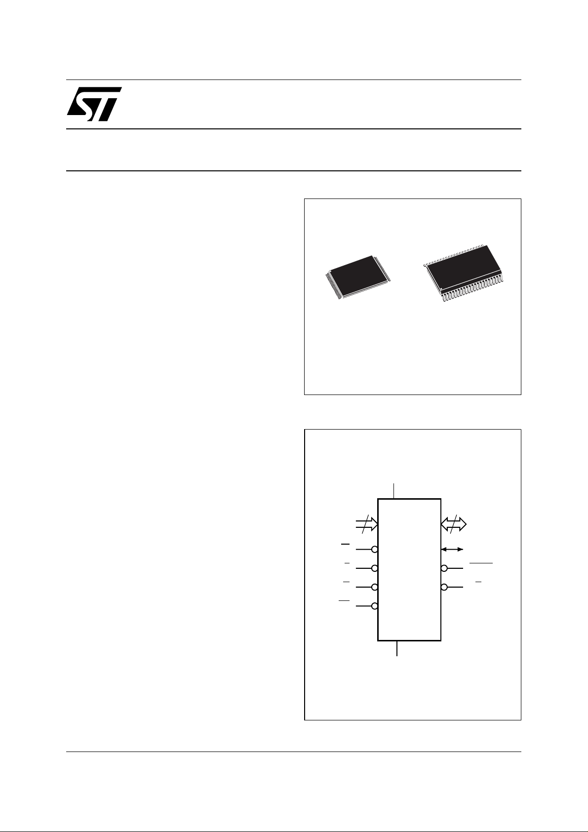
The memory is offered in TSOP4 8 (12 x 20mm)
and SO44 packages and it i s suppli ed with a ll the
bits erased (set to ’1’).
In order to meet environme ntal requirements, ST
offers the M29W200B in ECOPACK
®
packages.
ECOPACK packages are Lead-free. The category
of second Level Interconnect is marked on the
package and on the inner box label, in compliance
with JEDE C Stand ard JESD 97. The m aximum ratings related to soldering conditions are also
marked on the inner box label.
ECOPACK is an ST trademark. ECOPACK specifications are available at: www.st.com.
3/22

M29W200BT, M29W200BB
SIGNAL DESCRIPTIONS
See Figure 1, Logic Diag ra m, an d T ab le 1 , Signal
Names, for a brief overview of the signals connected to this device.
Address Inputs (A0-A16). The Address Inputs select the cells in the memory array to access during Bus Read operations. During Bus Write operations they control the commands sent to the Command Interface of the internal state machine.
Data Inputs/Outputs (DQ0-DQ7). The Data Inputs/Outputs output the data stored at the selected address during a Bus Read operation. During Bus Write operations they represent the commands sent to the Command Interface of the internal state machine.
Data Inputs/Outputs (DQ8-DQ14). The Data Inputs/Outputs output the data stored at the selected address during a Bus Read operation when BYTE is High, VIH. When BYTE is Low, VIL, these pins are not used and are high impedance. During Bus Write operations the Command Register does not use these bits. Wh en reading th e Status Re gister these bits should be ignored.
Data Input/Output or Address Input (DQ15A-1).
When BYTE
is High, VIH, this pin behaves as a
Data Input/Output pin (as DQ8-DQ14). When
BYTE
is Low, VIL, this pin behaves as an address
pin; DQ15A–1 Low will select the LSB of the Word
on the other addresses, DQ15A–1 High will select
the MSB. Throughout the text consider references
to the Data Input/Output to include th is pin when
BYTE
is High and references to the Ad dress Inputs to include this pin when BY TE
is Low except
when stated explicitly otherwise.
Chip Enable (E
). The Chip Enable, E, activates
the memory, allowing Bus Read and Bus Write operations to be performed. When Chip Enable is
High, V
Output Enable (G
, all other pins are ignored.
IH
). The Output Enable, G, con -
trols the Bus Read operation of the memory.
Write Enable (W
). The Write Enable, W, controls
the Bus Write operation of the memory’s Command Interface.
Reset/Block Temporary Unprotect (RP
). The Re-
set/Block Temporary Unprotect pin can be used to
apply a Hardware Reset to the memory or to temporarily unprotect all Blocks that have b een protected.
A Hardware Reset is achieved by holding Reset/
Block Temporary Unp rotect Low, V
. After Reset/Block Temporary Unprotect
t
PLPX
goes High, V
, the memory will be ready fo r Bus
IH
Read and Bus Write operations after t
, for at least
IL
PHEL
or
t
, whichever occurs last. See the Ready/Busy
RHEL
Output section, Table 17 and Figure 11, Reset/
Temporary Unprotect AC Characteristics for more
details.
Holding RP
at VID will temporarily unprotect the
protected Blocks in the memory. Program and
Erase operations on all blocks will be possible.
The transition from V
PHPHH
.
t
Ready/Busy Output (RB
to VID must be slower than
IH
). The Ready/Busy pin
is an open-drain output that can be used to identify
when the memory array can be read. Ready/Busy
is high-impedance during Read mode, Auto Select
mode and Erase Suspend mode.
After a Hardware Reset, Bus Read and Bus Write
operations cannot begin until Ready/Busy becomes high-impedan ce . S ee Tabl e 17 an d F i gure
11, Reset/Temporary Unprotect AC Characteristics.
During Program or Erase operations Re ady/Busy
is Low, V
. Ready/Busy will remain Lo w during
OL
Read/Reset commands o r Hardware Re sets until
the memory is ready to enter Read mode.
The use of an open-drain output allows the Ready/
Busy pins from several memories to be connected
to a single pull-up resistor. A Low will then indicate
that one, or more, of the memories is busy.
Byte/Word Organization Select (BYTE
). The Byte/
Word Organiza tion Se lect pin is used to swit ch between the 8-bit and 16-bit Bus modes of the memory. When Byte/Word Organi zatio n Selec t is Low,
V
, the memory is i n 8-bit mode, wh en it i s High,
IL
V
, the memory is in 16-bit mode.
IH
Supply Voltage. The VCC Supply Voltage
V
CC
supplies the power for all operations (Read, Program, Erase etc.).
The Command Interface is disabled when the V
CC
Supply Voltage is le ss than the Lockout Vo ltage,
. This prevents Bus Write operations from ac-
V
LKO
cidentally damaging the data during power up,
power down and power surges. If the Program/
Erase Controller is programming or erasing during
this time then the operation aborts and the memory contents being altered will be invalid.
A 0.1µF capacitor sh ould be connected between
the V
Supply Voltage pin and the VSS Ground
CC
pin to decouple the current surges from the power
supply. The PCB track widths must be sufficient to
carry the currents required during program and
erase operations, I
Ground. The VSS Ground is the reference for
V
SS
CC3
.
all voltage measurements.
4/22
M29W200BT, M29W200BB
BUS OPERATIONS
There are five standard bus operations that control
the device. These are Bus Read, Bus Writ e, Output Disable, Standby and Automatic Standby. See
Tables 5 and 6, Bus Operations, for a summary.
Typically glitches of les s th an 5ns on C hip Enab le
or Write Enable are ignored by the memory and do
not affect bus operations.
Bus Read. Bus Read operations read from the memory cells, or specific registers in the Command Interface. A valid Bus Read operation involves setting the desired address on the Address Inputs, applying a Low s ig nal, V
, to Chip Enable
IL
and Output Enable and keeping Write Enable
High, V
. The Data Inputs/Outputs will ou tpu t the
IH
value, see Figure 8, Read Mode AC Waveforms,
and Table 14, Read AC Characteristics, for details
of when the output becomes valid.
Bus Write. Bus Write operations write to the Command Interface. A v alid Bus Write operati on begins by setting the desired address on the Address Inputs. The Ad dress Inputs are latched b y the Command Interface on the falling edge of Chip
Table 5. Bus Operations, BYTE = V
Operation E G W
Bus Read
Bus Write
Output Disable X
Standby
Read Manufacturer
Code
Read Device Code
Note: X = VIL or VIH.
V
IL
V
IL
V
IH
V
IL
V
IL
IL
V
IL
V
IH
V
IH
X X X Hi-Z Hi-Z
V
IL
V
IL
V
Cell Address Hi-Z Data Output
IH
V
Command Address Hi-Z Data Input
IL
V
X Hi-Z Hi-Z
IH
A0 = VIL, A1 = VIL, A9 = VID,
V
IH
Others V
A0 = VIH, A1 = VIL, A9 = VID,
V
IH
Others V
Enable or Write Enable, whichever occurs last.
The Data Inputs/Outputs ar e latched by the Com mand Interface on the rising ed ge of Chip Enab le
or Write Enable, whichever occurs first. Output Enable must remain High, V
, during the whole Bus
IH
Write operation. See Figures 9 and 10, Write AC
Waveforms, and Tables 15 and 16, Write AC
Characteristics, for details of the timing requirements.
Output Disable. The Data Inputs /Outputs are in the high impedance state when Output Enable is High, V
.
IH
Standby. When Chip Enable is High, V memory enters Standby mode and the Data Inputs/Outputs pins are placed in the high-impedance state. To reduce the Su pply Current to the Standby Supply Current, I be held within V
± 0.2V. For the Standby current
CC
, Chip Enable should
CC2
level see Table 13, DC Characteristics.
During program or eras e operations the memory
will continue to use the Program/Erase Supply
Current, I
, for Program or Erase operations un-
CC3
til the operation completes.
Address Inputs
DQ15A–1, A0-A1 6
or V
IL
IH
or V
IL
IH
Data Inputs/Outputs
DQ14-DQ8 DQ7-DQ0
Hi-Z 20h
Hi-Z
51h (M29W200BT)
57h (M29W200BB)
IH
, the
Table 6. Bus Operations, BYTE = V
Operation E
Bus Read
Bus Write
Output Disable X
Standby
Read Manufacturer
Code
Read Device Code
Note: X = VIL or VIH.
V
IL
V
IL
V
IH
V
IL
V
IL
G W
V
IL
V
IH
V
IH
XXX Hi-Z
V
IL
V
IL
IH
Address Inputs
A0-A16
V
Cell Address Data Output
IH
V
Command Address Data Input
IL
V
XHi-Z
IH
A0 = VIL, A1 = VIL, A9 = VID,
V
IH
Others VIL or V
A0 = VIH, A1 = VIL, A9 = VID,
V
IH
Others VIL or V
IH
IH
Data Inputs/Outputs
DQ15A–1, DQ14-DQ0
0020h
0051h (M29W200BT)
0057h (M29W200BB)
5/22

M29W200BT, M29W200BB
Automatic Standby. If CMOS levels (VCC ± 0.2V)
are used to drive the bus and the bus is inactive for
150ns or more the memory enters Automatic
Standby where the interna l Supply Current is reduced to the Standby Supply Current, I
CC2
. The
Data Inputs/Outputs will still output data if a Bus
Read operation is in progress.
Special Bus Operations
Additional bus operations can be performed to
read the Electronic Signature and also to apply
and remove Block Protection. These bus operations are intended for us e by progr ammin g equip ment and are not usually used in applications.
They require V
to be applied to some pins.
ID
Electronic Signature. The memory has two codes, the manufacturer code and the device code, that can be read to identify the memory. These codes can b e read b y apply ing the sig nals listed in Tables 5 and 6, Bus Operations.
Block Protection and Blocks Unprotection. Each
block can be separately protected against accidental Program or Erase. Protected blocks can be
unprotected to allow data to be changed.
There are two methods available for protecting
and unprotecting the b locks, one for use on programming equipment and t he other for in-system
use. For further information refer to Application
Note AN1122, Applying Protectio n and Unpro tection to M29 Series Flash.
COMMAND INTERFACE
All Bus Write operations to the memory are interpreted by the Command Interface. Commands
consist of one or more sequential Bus Write operations. Failure to observe a valid sequence of Bus
Write operation s will result in the memory return ing to Read mode. The long command sequences
are imposed to maximize data security.
The address used for the commands changes depending on whether the memory is in 16-bit or 8bit mode. See either Ta ble 7, or 8, depending on
the configuration that is being used, for a summary
of the commands.
Read/Reset Command. The Read/Reset command returns the memory to its Read mode where it behaves lik e a ROM or EPROM. I t also resets the errors in the Status Register. Either one or three Bus Write o perations can be us ed to issue the Read/Reset command.
If the Read/Reset command is issued during a
Block Erase operation or following a Programming
or Erase error then the memory will take up to 10
µs
to abort. During the abort period no valid data can
be read from the memory. Issu ing a Read/Reset
command during a Block Erase operation will
leave invalid data in the memory.
Auto Select Command. The Auto Select command is used to read t he Manu facturer Code, the Device Code and the Block Protection Status. Three consecutive Bus Write operations are required to issue the Auto Sel ect command. Once the Auto Select comman d is issued the memory remains in Auto Sele ct mode until another command is issued.
From the Auto Select mode the Manufacturer
Code can be read using a Bus Read operation
with A0 = V
may be set to either V
and A1 = VIL. The other address bits
IL
or VIH. The Manufacturer
IL
Code for STMicroelectronics is 0020h.
The Device Code ca n be read using a Bu s Read
operation with A0 = V
address bits may be s et to either V
and A1 = VIL. The other
IH
or VIH. The
IL
Device Code for the M29W200BT is 0051h and for
the M29W200BB is 0057h.
The Block Protection Status of each block can be
read using a Bus Read oper ation with A0 = V
A1 = V
, and A12-A16 specifying the address of
IH
IL
the block. The other address bits may be set to either V
or VIH. If the addressed block is protected
IL
then 01h is output on Data Inputs/Outputs DQ0DQ7, otherwise 00h is output.
Program Command. The Program command can be used to program a value to one address in the memory array at a time. The command requires four Bus Write operations, the final write operation latches the address and data in the internal state machine and starts the Program/Erase Controller.
If the address falls in a protect ed block then the
Program command is ignored, the data remains
unchanged. The Status Register is never read and
no error condition is given.
During the program operation th e memory will ig nore all commands. It is no t possib le to is sue any
command to abort or pause the operation. Typical
program times are given in Table 9. Bus Read operations during the p rogram operation will output
the Status Register on the Data Inputs/Outputs.
See the section on the Status Register for more
details.
After the program operation has completed the
memory will return to the Read mode, unless an
error has occurred. When an error occurs the
memory will continue to output the Statu s Register. A Read/Reset command must be issued to reset the error condition and return to Read mode.
Note that the Program command cannot change a
bit set at ’0’ back t o ’1’. One of the Erase Commands must be used to set all the bits in a block or
in the whole memory from ’0’ to ’1’.
,
6/22
M29W200BT, M29W200BB
Table 7. Commands, 16-bit mode, BYTE = V
IH
Bus Write Operations
Command
Read/Reset
1X F0
3555 AA2AA 55 X F0
1st 2nd 3rd 4th 5th 6th
Length
Addr Data Addr Data Addr Data Addr Data Addr Data Addr Data
Auto Select 3 555 AA 2AA 55 555 90
Program 4 555 AA 2AA 55 555 A0 PA PD
Unlock Bypass 3 555 AA 2AA 55 555 20
Unlock Bypass
Program
2 X A0 PA PD
Unlock Bypass Reset 2 X 90 X 00
Chip Erase 6 555 AA 2AA 55 555 80 555 AA 2AA 55 555 10
Block Erase 6+ 555 AA 2AA 55 555 80 555 AA 2AA 55 BA 30
Erase Suspend 1 X B0
Erase Resume 1 X 30
Table 8. Commands, 8-bit mode, BYTE = V
IL
Bus Write Operations
Command
Read/Reset
1X F0
3 AAA AA 555 55 X F0
1st 2nd 3rd 4th 5th 6th
Length
Addr Data Addr Data Addr Data Addr Data Addr Data Addr Data
Auto Select 3 AAA AA 555 55 AAA 90
Program 4 AAA AA 555 55 AAA A0 PA PD
Unlock Bypass 3 AAA AA 555 55 AAA 20
Unlock Bypass
Program
2 X A0 PA PD
Unlock Bypass Reset 2 X 90 X 00
Chip Erase 6 AAA AA 555 55 AAA 80 AAA AA 555 55 AAA 10
Block Erase 6+ AAA AA 555 55 AAA 80 AAA AA 5 55 55 BA 30
Erase Suspend 1 X B0
Erase Resume 1 X 30
Note: X Don’t Care, PA Program Address, PD Program Data, BA Any address in the Block.
All values in the table are in hexadecimal.
The Command Interface only uses A–1, A0-A10 and DQ0-DQ7 to verify the commands; A11-A16, DQ8-DQ14 and DQ15 are Don’t Care.
DQ15A–1 is A–1 when BYTE
Read/Reset. After a Read/Reset c ommand, read the memory as normal until another command is issued. Auto Select. After an Auto Select command, read Manufacturer ID, Device ID or Block Protection Status. Program, Unlock Bypass Pr o gr am, Chip Erase, Block Erase. After these commands read the Status Register until the Program/Erase
Controller completes and the memory returns to Read Mode. Add additional Blocks during Block Erase Command wit h additional Bus Write
Operations until Timeout Bit is set.
Unlock Bypass. After the Unlock Bypass command issue Unlock Bypass Program or Unlock Bypass Reset commands. Unlock Bypass Reset. After the Unlock By pass Reset command read the memory as normal until another command is issued. Erase Suspend. After the Erase Suspend co mmand read non-erasing memory blocks as nor mal, issue Auto Select and P rogram commands
on non-erasing blocks as normal. Erase Resume. After the Erase Resume command the suspended Erase operation resumes, read the Status Register until the Program/
Erase Controller completes and the memory returns to Read Mode.
is VIL or DQ15 when BYTE is VIH.
7/22
 Loading...