

ST M29F400BT, M29F400BB User Manual
查询M295V400BB45M1T供应商
4 Mbit (512Kb x8 or 256Kb x16, Boot Block)
■ SINGLE 5V±10% SUPPL Y VOLTAGE for
PROGRAM, ERAS E and READ O PER AT IONS
■ ACCESS TIME: 45ns
■ PROGRAMMING TIME
– 8µs per Byte/Word typical
■ 11 MEMORY BLOCKS
– 1 Boot Block (Top or Bottom Location)
– 2 Parameter and 8 Main Blocks
■ PROGRAM/ERA SE CON T ROL LER
– Embedded Byte/Word Program algorithm
– Embedded Multi-Block/Chip Erase algorithm
– Status Register Polling and Toggle Bits
– Ready/Busy Output Pin
■ ERASE SUSPEND and RESUME MODES
– Read and Program another Block during
Erase Suspend
■ UNLOCK BYPASS PROGRAM COMMAND
– Faster Production/Batch Programming
■ TEMPORARY BLOCK UNPROTECTION
MODE
■ LOW POWER CONSUMPTION
– Standby and Automatic Standby
■ 100,000 PROGRAM/ER ASE CYCL ES per
BLOCK
■ 20 YEARS DATA RETENTI ON
– Defectivity below 1 ppm/year
■ ELECTRONIC SIGNATURE
– Manufacturer Code: 0020h
– Top Device Code M29F400BT: 00D5h
– Bottom Device Code M29F400BB: 00D6h
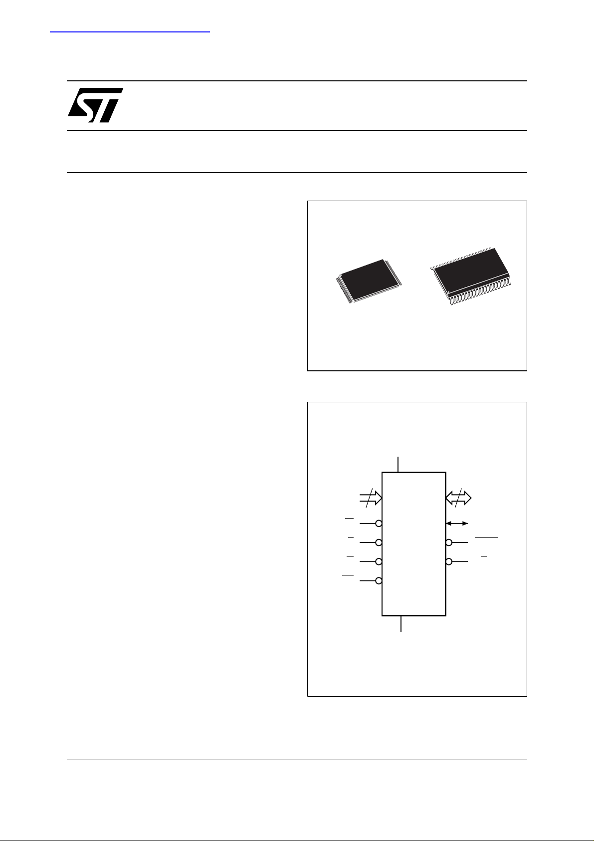
M29F400BT
M29F400BB
Single Supply Flash Memory
44
1
TSOP48 (N)
12 x 20mm
Figure 1. Logic Diagram
V
CC
18
A0-A17
W
E
G
RP
M29F400BT
M29F400BB
V
SS
SO44 (M)
15
DQ0-DQ14
DQ15A–1
BYTE
RB
AI02904
1/22July 2000
M29F400BT, M29F400BB
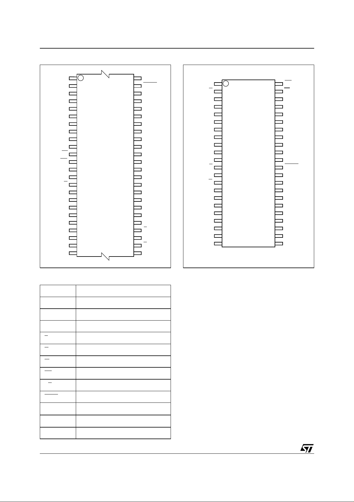
Figure 2. TSOP Connections
A15
A14
A13
A12
A11
A10 DQ14
A9
A8
NC
NC
RP
NC
NC
RB
NC
A17
A7
A6
A5
A4
A3
A2
A1
1
W
12
M29F400BT
M29F400BB
13
24 25
48
37
36
AI02905
A16
BYTE
V
SS
DQ15A–1
DQ7
DQ6
DQ13
DQ5
DQ12
DQ4
V
CC
DQ11
DQ3
DQ10
DQ2
DQ9
DQ1
DQ8
DQ0
G
V
SS
E
A0
Figure 3. SO Connections
NC RP
A17 A8
A7
A6
A5
A4
A3
A2
A1
A0
V
SS
DQ0
DQ8
DQ9
DQ10
DQ3
DQ11
1
2
3
4
5
6
7
8
9
10
11
M29F400BT
M29F400BB
12
E
13
14
G
15
16
17DQ1
18
19
20
21
44
43
42
41
40
39
38
37
36
35
34
33
32
31
30
29
28
27
26
25
24
2322
AI02906
WRB
A9
A10
A11
A12
A13
A14
A15
A16
BYTE
V
SS
DQ15A–1
DQ7
DQ14
DQ6
DQ13
DQ5DQ2
DQ12
DQ4
V
CC
Table 1. Signal Names
A0-A17 Address Inputs
DQ0-DQ7 Data Inputs/Outputs
DQ8-DQ14 Data Inputs/Outputs
DQ15A–1 Data Input/Output or Address Input
E
G
W
RP
RB
BYTE
V
CC
V
SS
NC Not Connected Internally
2/22
Chip Enable
Output Enable
Write Enable
Reset/Block Temporary Unprotect
Ready/Busy Output
Byte/Word Organization Select
Supply Voltage
Ground
SUMMARY DESCRIPTION
The M29F400B is a 4 Mbit (512Kb x8 or 256Kb
x16) non-volatile memory that can be read, erased
and reprogrammed. These operations can be performed using a single 5V supply. On power-up the
memory defaults to its Read mode where it can be
read in the same way as a ROM or EPROM. The
M29F400B is fully backward comp atible with the
M29F400.
The memory is divided into blocks that can be
erased independently so it is pos sible to pres erve
valid data while old data is erased. Each block can
be protected independently to prev ent accidental
Program or Erase commands from modifying the
memory. Program and Erase com m ands are wri tten to the Command Interface of t he memory. An
on-chip Program/Erase Controller simplifies the
process of programming or erasing the memory by
taking care of all of the special operations that are
required to update the memory contents. The end
of a program or erase op eration can be de tected
and any error conditions identified. The command
set required to control the memory is consistent
with JEDEC standards.
M29F400BT, M29F400BB
Table 2. Absolute Maximum Ratings
Symbol Parameter Value Unit
Ambient Operating Temperature (Temperature Range Option 1) 0 to 70 °C
T
A
T
BIAS
T
STG
(2)
V
IO
V
CC
V
ID
Note: 1. Except for the ratin g "Operating Temperat ure Range", stresses above those listed i n t he Table "Absolute M aximum Rat i ngs" may
cause permanent damage to the device. These are stress ratings only and operation of the device at these or any other conditions
above those indi cated in t he Operat in g sections of this specifi cation i s not impl i ed. Exposure to Absolute Maximum Rating c onditions for extended per iods may aff ect device reliabilit y. Refer also to the STMicroel ectronics SURE Program an d other relevan t qual ity docum en ts .
2. Mini m um Voltage ma y undershoot to –2V during transiti on and for less than 20ns duri ng transitio ns.
Ambient Operating Temperature (Temperature Range Option 6) –40 to 85 °C
Ambient Operating Temperature (Temperature Range Option 3) –40 to 125 °C
Temperature Under Bias –50 to 125 °C
Storage Temperature –65 to 150 °C
Input or Output Voltage –0.6 to 6 V
Supply Voltage –0.6 to 6 V
Identification Voltage –0.6 to 13.5 V
The blocks in the memory are as ymmetrically arranged, see Tables 3 and 4, Block Addresses. The
first or last 64 Kbytes have been divide d into four
additional blocks. The 16 Kbyte Boot Block can be
used for small initialization code to start the microprocessor, the two 8 Kbyte Parameter Blocks can
be used for parameter storage and the rem aining
(1)
Chip Enable, Output Enable and Write Enable signals control the bus operation of the memory.
They allow simple conne ction to most microprocessors, often without additional logic.
The memory is offered in TSOP48 (12 x 20mm)
and SO44 packa ges and it is supplied with all t he
bits erased (set to ’1’).
32K is a small Main Block where the application
may be stored.
Table 3. Top Boot Block Addresses,
M29F400BT
Size
#
(Kbyte
s)
10 16 7C000h-7FFFFh 3E000h-3FFFFh
9 8 7A000h-7BFFFh 3D000h-3DFFFh
8 8 78000h-79FFFh 3C000h-3CFFFh
7 32 70000h-77FFFh 38000h-3BFFFh
6 64 60000h-6FFFFh 30000h-37FFFh
5 64 50000h-5FFFFh 28000h-2FFFFh
4 64 40000h-4FFFFh 20000h-27FFFh
3 64 30000h-3FFFFh 18000h-1FFFFh
2 64 20000h-2FFFFh 10000h-17FFFh
1 64 10000h-1FFFFh 08000h-0FFFFh
0 64 00000h-0FFFFh 00000h-07FFFh
Address Range
(x8)
Address Range
(x16)
Table 4. Bottom Boot Block addresses,
M29F400BB
Size
#
(Kbyte
s)
10 64 70000h-7FFFFh 38000h-3FFFFh
9 64 60000h-6FFFFh 30000h-37FFFh
8 64 50000h-5FFFFh 28000h-2FFFFh
7 64 40000h-4FFFFh 20000h-27FFFh
6 64 30000h-3FFFFh 18000h-1FFFFh
5 64 20000h-2FFFFh 10000h-17FFFh
4 64 10000h-1FFFFh 08000h-0FFFFh
3 32 08000h-0FFFFh 04000h-07FFFh
2 8 06000h-07FFFh 03000h-03FFFh
1 8 04000h-05FFFh 02000h-02FFFh
0 16 00000h-03FFFh 00000h-01FFFh
Address Range
(x8)
Address Range
(x16)
3/22

M29F400BT, M29F400BB
SIGNAL DESCRIPTIONS
See Figure 1, Logic Diagram, and Table 1, Sign al
Names, for a brief overview of the signals connected to this device.
Address Inputs (A0-A17). The Address Inputs
select the cells i n the memory array to a ccess during Bus Read operations. During Bus Write operations they control the commands sent to the
Command Interface of the internal state machine.
Data Inputs/Outputs (DQ0-DQ7). The Data Inputs/Outputs output the data stored at the selected
address during a Bus Read operation. During Bus
Write operations they represent the commands
sent to the Command Interface of the internal state
machine.
Data Inputs/Outputs (DQ8-DQ14). The Data Inputs/Outputs output the data stored at the selected
address during a Bus Read operation when BYTE
is High, VIH. When BYTE is Low, VIL, these pins
are not used and are high impedance. During Bus
Write operations the Command Register does not
use these bits. When reading t he Status Register
these bits should be ignored.
Data Input/Output or Address Input (DQ15A-1).
When BYTE
is High, VIH, this pin behaves as a
Data Input/Output pin (as DQ8-DQ14). When
is Low, VIL, this pin behaves as an address
BYTE
pin; DQ15A–1 Low will select the LSB of the Word
on the other addresses, DQ15A–1 High will select
the MSB. Throughout the text consider references
to the Data Input/Output to include this pin when
BYTE
is High and ref erences to the Address In-
puts to include this pin when BYTE
is Low except
when stated explicitly otherwise.
Chip Enable (E
). The Chip Enable, E, activates
the memory, allowing Bus Read and Bus Write operations to be performed. When Chip Enable is
High, V
Output Enable (G
, all other pins are ignored.
IH
). The Output Enable, G, con-
trols the Bus Read operation of the memory.
Write Enable (W
). The Write Enable, W, controls
the Bus Write operation of the memory’s Command Interf a c e .
Reset/Bloc k Tempor ary U nprot ect (RP
). The Re-
set/Block Temporary Unprotect pin can be used to
apply a Hardware Reset to the memory or to temporarily unprotect all Blocks that have been protected.
A Hardware Reset is achieved by holding Reset/
Block Temporary Unprotect Low, V
t
. After Reset/Block Temporary Unprotect
PLPX
goes High, V
, the memory will be ready for Bus
IH
Read and Bus Write operations after t
, for at least
IL
PHEL
or
, whichever occurs last. See the Ready/Busy
t
RHEL
Output section, Table 17 and Figure 11, Reset/
Temporary Unprotect AC Characteristics for more
details.
Holding RP
at VID will temporarily unprotect the
protected Blocks in the memory. Program and
Erase operations on all blocks will be possible.
The transition from V
PHPHH
.
t
Ready/Busy Output (RB
to VID must be slower than
IH
). The Ready/Busy pin
is an open-drain output that can be used to identify
when the memory array can be read. Ready/Busy
is high-impedance during Read mode, Auto Select
mode and Erase Suspend mode.
After a Hardware Reset, Bus Read and Bus Write
operations cannot begin until Ready/Busy becomes high-impedance. See Tabl e 17 and Figure
11, Reset/Temporary Unprotect AC Ch aracteristics.
During Program or Erase operations Ready/Busy
is Low, V
. Ready/Busy will remain Low during
OL
Read/Reset commands or Hardw are Resets until
the memory is ready to enter Read mode.
The use of an open-drain output allows the Ready/
Busy pins from several memories to be connected
to a single pull-up resistor. A Low will then indicate
that one, or more, of the memories is busy.
Byte/Word Or ga nizat ion Select (BYTE
). The Byte/
Word Organization Select pin is used to switch between the 8-bit and 16-bit Bus modes of the memory. When Byte/Word Organi z ation S elect is Low,
V
, the memory is in 8-bi t mode, w hen it is High,
IL
V
, the memory is in 16-bit mode.
IH
Supply Voltage. The VCC Supply Voltage
V
CC
supplies the power for all operations (Read, Program, Erase etc.).
The Command Interface is disabled when the V
CC
Supply Voltage is less than the L ockout Voltage,
. This prevents Bus Write operations from ac-
V
LKO
cidentally damaging the data during power up,
power down and power surges. If the Program/
Erase Controller is programming or erasing during
this time then the operation aborts and the memory contents being altered will be invalid.
A 0.1µF capacitor should be connected between
the V
Supply Voltage pin and the VSS Ground
CC
pin to decouple the current surges from the power
supply. The PCB track widths must be sufficient to
carry the currents required during program and
erase operations, I
Vss Ground. The V
.
CC4
Ground is the reference
SS
for all voltage measurements.
4/22
M29F400BT, M29F400BB
BUS OPERATIONS
There are five standard bus operations that control
the device. These are Bus Read, Bus Wri te, Output Disable, Standby and Automatic Standby. See
Tables 5 and 6, Bus Operat ions, for a summary.
Typically glitches of less than 5ns on Chip Enable
or Write Enable are ignored by the memory and do
not affect bus operations.
Bus Read. Bus Read operations read from the
memory cells, or specific registers in the Command Interface. A valid Bus Read operation involves setting the desired address on the Address
Inputs, applying a Low sig nal, V
, to Chip Enable
IL
and Output Enable and keeping Write Enable
High, V
. The Data Inputs/Outputs will output the
IH
value, see Figure 8, Rea d Mode AC Wav eforms,
and Table 14, Read AC Characteristics, for details
of when the output becomes valid.
Bus Write. Bus Write operations write to the
Command Interface. A valid Bus Write operation
begins by setting the desire d address on t he Address Inputs. The Address Inputs are latched by
the Command Interface on the falling edge of Chip
Enable or Write Enable, whichever occurs last.
The Data Inputs/Outputs a re latched by the Com-
mand Interface on the rising edge of Chip Enable
or Write Enable, whichever occurs first. Output Enable must remain High, V
, during the whole Bus
IH
Write operation. See Figures 9 and 10, Write AC
Waveforms, and Tables 15 and 16, Write AC
Characteristics, for details of the timing requirements.
Output Disa bl e . The Data Inputs/Outputs are in
the high impedance s tate when Output Enable is
High, V
Standby. When Chip Enable is High, V
.
IH
, the
IH
Data Inputs/Outputs pins are placed in the highimpedance state and the Supply Current is reduced to the Standby level.
When Chip Enable is at V
reduced to the TTL Standby Supply Current, I
the Supply Current is
IH
CC2
To further reduce the Supply Current to the CMOS
Standby Supply Current, I
be held within V
± 0.2V. For Standby current
CC
, Chip Enable should
CC3
levels see Table 13, DC Characteristics.
During program or erase operations the memory
will continue to use the Program/Erase Supply
Current, I
, for Program or Erase operations un-
CC4
til the operation completes.
.
Table 5. Bus Operations, BYTE = V
Operation E G W
Bus Read
Bus Write
Output Disable X
Standby
Read Manufacturer
Code
Read Device Code
Note: X = VIL or VIH.
V
IL
V
IL
V
IH
V
IL
V
IL
V
IL
V
IH
V
IH
X X X Hi-Z Hi-Z
V
IL
V
IL
Table 6. Bus Operations, BYTE = V
Operation E
Bus Read
Bus Write
Output Disable X
Standby
Read Manufacturer
Code
Read Device Code
Note: X = VIL or VIH.
V
IL
V
IL
V
IH
V
IL
V
IL
G W
V
IL
V
IH
V
IH
X X X Hi-Z
V
IL
V
IL
IL
Address Inputs
DQ15A–1, A0-A1 7
V
Cell Address Hi-Z Data Output
IH
V
Command Address Hi-Z Data Input
IL
V
X Hi-Z Hi-Z
IH
A0 = VIL, A1 = VIL, A9 = VID,
V
IH
Others V
A0 = VIH, A1 = VIL, A9 = VID,
V
IH
Others V
IH
V
Cell Address Data Output
IH
V
Command Address Data Input
IL
V
X Hi-Z
IH
A0 = VIL, A1 = VIL, A9 = VID,
V
IH
Others V
A0 = VIH, A1 = VIL, A9 = VID,
V
IH
Others V
or V
IL
IH
or V
IL
IH
Address Inputs
A0-A17
or V
IL
IH
or V
IL
IH
Data Inputs/Outputs
DQ14-DQ8 DQ7-DQ0
Hi-Z 20h
Hi-Z
Data Inputs/Outputs
DQ15A–1, DQ14-DQ0
00D5h (M29F400B T)
00D6h (M29F400B B)
D5h (M29F400BT)
D6h (M29F400BB)
0020h
5/22

M29F400BT, M29F400BB
Auto m ati c S tan d by . If CMOS levels (VCC ± 0.2V)
are used to drive the bus and the bus is inactive for
150ns or more the memory enters Automatic
Standby where the internal Supply Current is reduced to the CMOS Standby Supply Current, I
CC3
The Data In puts/Outputs will s till output data if a
Bus Read operation is in progress.
Special Bus Operations
Additional bus operations can be performed to
read the Electronic Signature and also to apply
and remove Block Protec tion. These bus operations are intended for use by programming equipment and are not usually used in applications.
They require V
to be applied to some pins.
ID
Electronic Signature. The memory has two
codes, the manufacturer code and the device
code, that can be read to identify the memory.
These codes can be read by applying t he signals
listed in Tables 5 and 6, Bus Operations.
Block Protection and Blocks Unprotection. Each
block can be separately protected against accidental Program or Erase. Protected blocks can be
unprotected to allow data to be changed.
There are two methods available for protecting
and unprotecting the blocks, one for use on programming equipment and the other for in-system
use. For further information refer to Application
Note AN1122, Applying P rotection and Unp rotection to M29 Series Flash.
COMMAND INTERFACE
All Bus Write operations t o the me mory are in terpreted by the Command Interface. Commands
consist of one or more sequential Bus Write oper-
.
ations. Failure to observe a valid sequence of Bus
Write operations will result in the memory returning to Read mode. The long command sequences
are imposed to maximize data security.
The address used for the commands changes depending on whether the memory is in 16-bit or 8bit mode. See either Table 7, or 8, de pending on
the configuration that is being used, for a summary
of the commands.
Read/Reset Command. The Read/Reset command returns the memory to its Read mode where
it behaves like a ROM or EPROM. It also resets
the errors in the Status Register. Either one or
three Bus Write operations can be u sed to issue
the Read/Reset command.
If the Read/Reset command is issued during a
Block Erase operation or following a Programming
or Erase error then the memory will take upto 10
to abort. During the abort period no valid data can
be read from the memory. Issuing a Read/Reset
command during a Block Erase operation will
leave invalid data in the memory.
Auto Select Command. The Auto Select command is used to read the Manufacturer Code, the
Device Code and the Block Protection Status.
Three consecutive Bus Write operations are required to issue the Auto Select command. Once
the Auto Select comma nd is issued the memory
remains in Auto Select mode unt il another command is issued.
From the Auto Select mode the Manufacturer
Code can be read using a Bus Read operation
with A0 = V
may be set to either V
and A1 = VIL. The other address bits
IL
or VIH. The Manufa cturer
IL
Code for STMicroelectronics is 0020h.
The Device Code can be read using a B us Read
operation with A0 = V
address bits may be set to e ither V
and A1 = VIL. The other
IH
IL
Device Code for the M29F400BT is 00D5h and for
the M29F400BB is 00D6h.
µs
or VIH. The
6/22
M29F400BT, M29F400BB
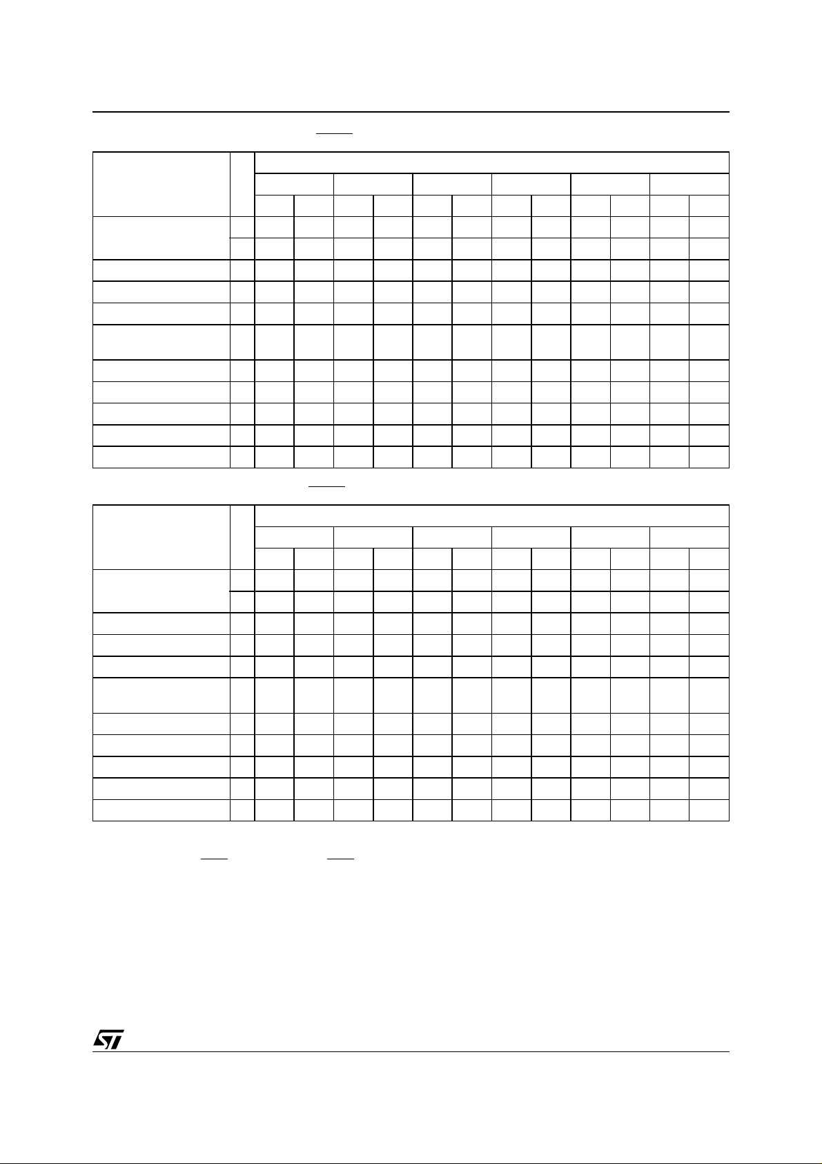
Table 7. Commands, 16-bit mode, BYTE = V
IH
Bus Write Operations
Command
Read/Reset
1X F0
3 555 AA 2AA 55 X F0
1st 2nd 3rd 4th 5th 6th
Length
Addr Data Addr Data Addr Data Addr Data Addr Data Addr Data
Auto Select 3 555 AA 2AA 55 555 90
Program 4 555 AA 2AA 55 555 A0 PA PD
Unlock Bypass 3 555 AA 2AA 55 555 20
Unlock Bypass
Program
2X A0PAPD
Unlock Bypass Reset 2 X 90 X 00
Chip Erase 6 555 AA 2AA 55 555 80 555 AA 2AA 55 555 10
Block Erase 6+ 555 AA 2AA 55 555 80 555 AA 2AA 55 BA 30
Erase Suspend 1 X B0
Erase Resume 1 X 30
Table 8. Commands, 8-bit mode, BYTE = V
IL
Bus Write Operations
Command
Read/Reset
1X F0
3 AAA AA 555 55 X F0
1st 2nd 3rd 4th 5th 6th
Length
Addr Data Addr Data Addr Data Addr Data Addr Data Addr Data
Auto Select 3 AAA AA 555 55 AAA 90
Program 4 AAA AA 555 55 AAA A0 PA PD
Unlock Bypass 3 AAA AA 555 55 AAA 20
Unlock Bypass
Program
2X A0PAPD
Unlock Bypass Reset 2 X 90 X 00
Chip Erase 6 AAA AA 555 55 AAA 80 AAA AA 555 55 AAA 10
Block Erase 6+ AAA AA 555 55 AAA 80 AAA AA 555 55 BA 30
Erase Suspend 1 X B0
Erase Resume 1 X 30
Note: X Don’t Care, PA Program Address, PD Program Data, BA Any address in the Block.
All values in the table are in hexadecimal.
The Command Interface only uses A–1, A0-A10 and DQ0-DQ7 to verify the commands; A11-A17, DQ8-DQ14 and DQ15 are Don’t Care.
DQ15A–1 is A–1 when BYTE
Read/Reset. After a Read/Reset command, read the memory as normal until another command is issued.
Auto Select. After an A uto Select command, read Manufactu rer ID, Device ID or Block P rot ection Status.
Program, Unlock Bypass Program, Ch i p Erase, Blo ck E r ase. After these command s read t he St atus R egister until the Pro gram/Er ase
Controller complet es and the mem ory returns to Read Mode. Ad d additional Blocks dur in g Block Erase Command with additio nal B us Write
Operations until Timeout Bit is set.
Unlock Bypass. After the Unlock Bypass command issue Unlock Bypass Program or Unlock Bypass Reset commands.
Unlock Bypass Reset. After the Unlock Bypass Reset command read the memory as normal until another command is issued.
Erase Suspend. After the Erase Suspend command read non-erasing memory blocks as normal, issue Auto Select and Program commands
on non-era sing blocks as normal.
Erase Resume. After the E ras e Res ume c omman d the s uspe nde d Er ase o pe ration re sum es, read th e Stat u s Reg ister u ntil the Prog ram/
Erase Cont roller compl etes and th e m em ory retur ns to Read Mode.
is VIL or DQ15 wh en BYTE is VIH.
7/22
 Loading...