

Page 1
FEATURES SUMMARY
■ SUPPLY VOLTAGE
–V
5V ±10% for PROGRAM, ERASE and
CC =
READ OPERATIONS
■ ACCESS TIME: 55, 70, 90ns
■ PROGRAMMING TIME
– 10µs per Byte typical
■ 16 UNIFORM 64Kbyte MEMORY BLOCKS
■ PROGRAM/ERASE CONTROLLER
– Embedded Byte Program algorithms
■ ERASE SUSPEND and RESUME MODES
– Read and Program another Block during
Erase Suspend
■ UNLOCK BYPASS PROGRAM COMMAND
– Faster Production/Batch Programming
■ TEMPORARY BLOCK UNPROTECTION
MODE
■ COMMON FLASH INTERFACE
– 64 bit Security Code
■ LOW POWER CONSUMPTION
– Standby and Automatic Standby
■ 100,000 PROGRAM/ERASE CYCLES per
BLOCK
■ ELECTRONIC SIGNATURE
– Manufacturer Code : 20h
– Device Code: F1h
■ ECOPACK
®
PACKAGES AVAILABLE
M29F080D
8 Mbit (1Mb x8, Uniform Block)
5V Supply Flash Memory
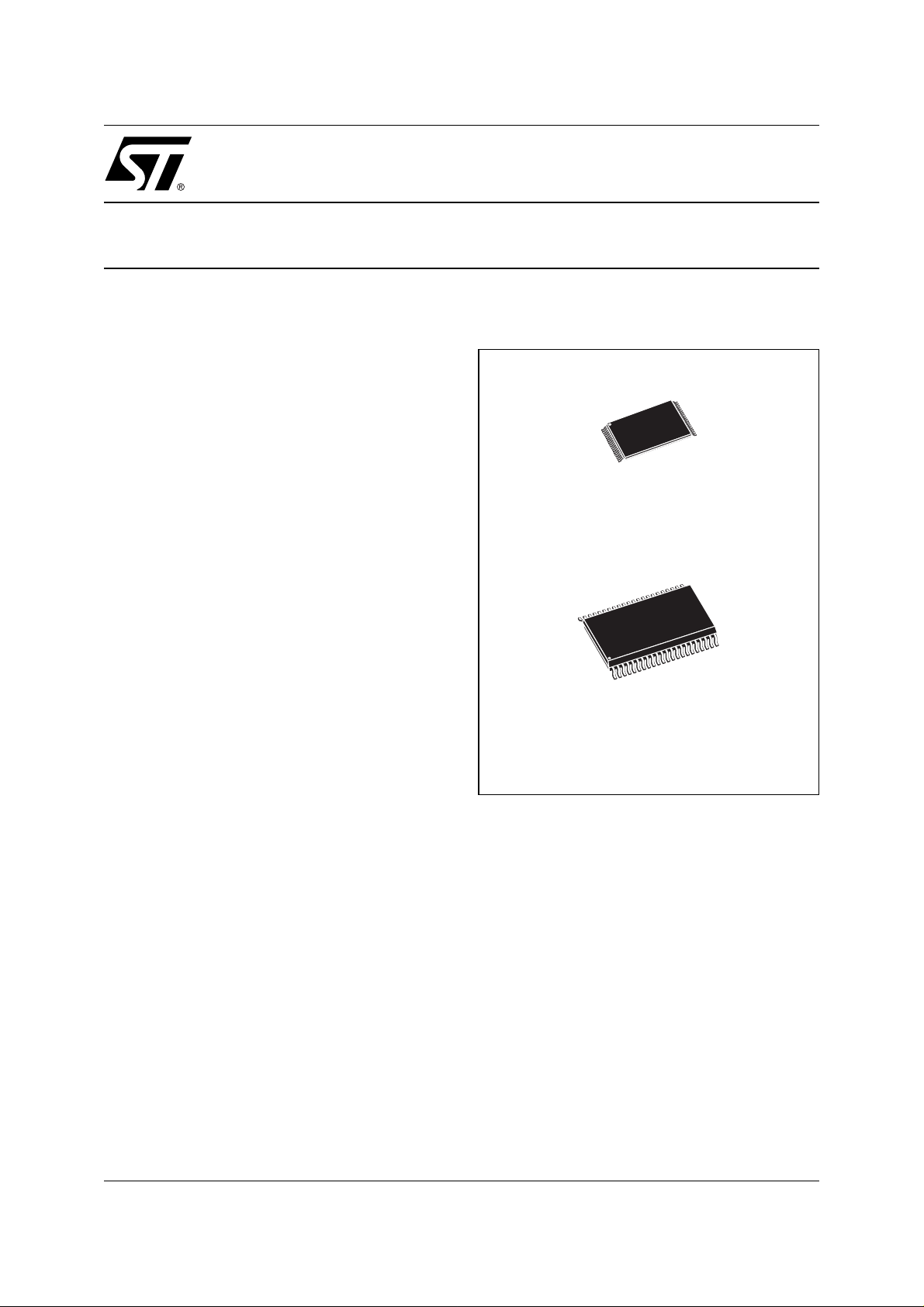
Figure 1. Packages
TSOP40 (N)
10 x 20mm
SO44 (M)
1/37September 2005
Page 2

M29F080D
TABLE OF CONTENTS
SUMMARY DESCRIPTION. . . . . . . . . . . . . . . . . . . . . . . . . . . . . . . . . . . . . . . . . . . . . . . . . . . . . . . . . . . 5
Figure 2. Logic Diagram . . . . . . . . . . . . . . . . . . . . . . . . . . . . . . . . . . . . . . . . . . . . . . . . . . . . . . . . . . 5
Table 1. Signal Names . . . . . . . . . . . . . . . . . . . . . . . . . . . . . . . . . . . . . . . . . . . . . . . . . . . . . . . . . . . 5
Figure 3. TSOP Connections. . . . . . . . . . . . . . . . . . . . . . . . . . . . . . . . . . . . . . . . . . . . . . . . . . . . . . . 6
Figure 4. SO Connections. . . . . . . . . . . . . . . . . . . . . . . . . . . . . . . . . . . . . . . . . . . . . . . . . . . . . . . . . 6
Figure 5. Block Addresses. . . . . . . . . . . . . . . . . . . . . . . . . . . . . . . . . . . . . . . . . . . . . . . . . . . . . . . . . 7
SIGNAL DESCRIPTIONS . . . . . . . . . . . . . . . . . . . . . . . . . . . . . . . . . . . . . . . . . . . . . . . . . . . . . . . . . . . . 8
Address Inputs (A0-A19). . . . . . . . . . . . . . . . . . . . . . . . . . . . . . . . . . . . . . . . . . . . . . . . . . . . . . . . . . 8
Data Inputs/Outputs (DQ0-DQ7). . . . . . . . . . . . . . . . . . . . . . . . . . . . . . . . . . . . . . . . . . . . . . . . . . . . 8
Chip Enable (E). . . . . . . . . . . . . . . . . . . . . . . . . . . . . . . . . . . . . . . . . . . . . . . . . . . . . . . . . . . . . . . . . 8
Output Enable (G). . . . . . . . . . . . . . . . . . . . . . . . . . . . . . . . . . . . . . . . . . . . . . . . . . . . . . . . . . . . . . . 8
Write Enable (W). . . . . . . . . . . . . . . . . . . . . . . . . . . . . . . . . . . . . . . . . . . . . . . . . . . . . . . . . . . . . . . . 8
Reset/Block Temporary Unprotect (RP).. . . . . . . . . . . . . . . . . . . . . . . . . . . . . . . . . . . . . . . . . . . . . .8
Ready/Busy Output (RB). . . . . . . . . . . . . . . . . . . . . . . . . . . . . . . . . . . . . . . . . . . . . . . . . . . . . . . . . . 8
V
Supply Voltage (5V). . . . . . . . . . . . . . . . . . . . . . . . . . . . . . . . . . . . . . . . . . . . . . . . . . . . . . . . . . 8
CC
V
Ground. . . . . . . . . . . . . . . . . . . . . . . . . . . . . . . . . . . . . . . . . . . . . . . . . . . . . . . . . . . . . . . . . . . . 8
SS
BUS OPERATIONS. . . . . . . . . . . . . . . . . . . . . . . . . . . . . . . . . . . . . . . . . . . . . . . . . . . . . . . . . . . . . . . . . 9
Bus Read. . . . . . . . . . . . . . . . . . . . . . . . . . . . . . . . . . . . . . . . . . . . . . . . . . . . . . . . . . . . . . . . . . . . . . 9
Bus Write. . . . . . . . . . . . . . . . . . . . . . . . . . . . . . . . . . . . . . . . . . . . . . . . . . . . . . . . . . . . . . . . . . . . . . 9
Output Disable. . . . . . . . . . . . . . . . . . . . . . . . . . . . . . . . . . . . . . . . . . . . . . . . . . . . . . . . . . . . . . . . . . 9
Standby. . . . . . . . . . . . . . . . . . . . . . . . . . . . . . . . . . . . . . . . . . . . . . . . . . . . . . . . . . . . . . . . . . . . . . . 9
Automatic Standby. . . . . . . . . . . . . . . . . . . . . . . . . . . . . . . . . . . . . . . . . . . . . . . . . . . . . . . . . . . . . . . 9
Special Bus Operations . . . . . . . . . . . . . . . . . . . . . . . . . . . . . . . . . . . . . . . . . . . . . . . . . . . . . . . . . 9
Electronic Signature. . . . . . . . . . . . . . . . . . . . . . . . . . . . . . . . . . . . . . . . . . . . . . . . . . . . . . . . . . . . . . 9
Block Protection and Blocks Unprotection. . . . . . . . . . . . . . . . . . . . . . . . . . . . . . . . . . . . . . . . . . . . .9
Table 2. Bus Operations . . . . . . . . . . . . . . . . . . . . . . . . . . . . . . . . . . . . . . . . . . . . . . . . . . . . . . . . . . 9
COMMAND INTERFACE . . . . . . . . . . . . . . . . . . . . . . . . . . . . . . . . . . . . . . . . . . . . . . . . . . . . . . . . . . . 10
Read/Reset Command. . . . . . . . . . . . . . . . . . . . . . . . . . . . . . . . . . . . . . . . . . . . . . . . . . . . . . . . . . . 10
Auto Select Command. . . . . . . . . . . . . . . . . . . . . . . . . . . . . . . . . . . . . . . . . . . . . . . . . . . . . . . . . . . 10
Program Command. . . . . . . . . . . . . . . . . . . . . . . . . . . . . . . . . . . . . . . . . . . . . . . . . . . . . . . . . . . . . 10
Unlock Bypass Command. . . . . . . . . . . . . . . . . . . . . . . . . . . . . . . . . . . . . . . . . . . . . . . . . . . . . . . . 10
Unlock Bypass Program Command. . . . . . . . . . . . . . . . . . . . . . . . . . . . . . . . . . . . . . . . . . . . . . . . . 10
Unlock Bypass Reset Command. . . . . . . . . . . . . . . . . . . . . . . . . . . . . . . . . . . . . . . . . . . . . . . . . . .10
Chip Erase Command. . . . . . . . . . . . . . . . . . . . . . . . . . . . . . . . . . . . . . . . . . . . . . . . . . . . . . . . . . . 11
Block Erase Command.. . . . . . . . . . . . . . . . . . . . . . . . . . . . . . . . . . . . . . . . . . . . . . . . . . . . . . . . . . 11
Erase Suspend Command. . . . . . . . . . . . . . . . . . . . . . . . . . . . . . . . . . . . . . . . . . . . . . . . . . . . . . . . 11
Erase Resume Command. . . . . . . . . . . . . . . . . . . . . . . . . . . . . . . . . . . . . . . . . . . . . . . . . . . . . . . . 12
Read CFI Query Command. . . . . . . . . . . . . . . . . . . . . . . . . . . . . . . . . . . . . . . . . . . . . . . . . . . . . . . 12
Block Protect and Chip Unprotect Commands. . . . . . . . . . . . . . . . . . . . . . . . . . . . . . . . . . . . . . . . . 12
Table 3. Commands . . . . . . . . . . . . . . . . . . . . . . . . . . . . . . . . . . . . . . . . . . . . . . . . . . . . . . . . . . . . 13
2/37
Page 3

M29F080D
Table 4. Program, Erase Times and Program, Erase Endurance Cycles . . . . . . . . . . . . . . . . . . . . 13
STATUS REGISTER . . . . . . . . . . . . . . . . . . . . . . . . . . . . . . . . . . . . . . . . . . . . . . . . . . . . . . . . . . . . . . . 14
Data Polling Bit (DQ7). . . . . . . . . . . . . . . . . . . . . . . . . . . . . . . . . . . . . . . . . . . . . . . . . . . . . . . . . . . 14
Toggle Bit (DQ6).. . . . . . . . . . . . . . . . . . . . . . . . . . . . . . . . . . . . . . . . . . . . . . . . . . . . . . . . . . . . . . . 14
Error Bit (DQ5). . . . . . . . . . . . . . . . . . . . . . . . . . . . . . . . . . . . . . . . . . . . . . . . . . . . . . . . . . . . . . . . . 14
Erase Timer Bit (DQ3). . . . . . . . . . . . . . . . . . . . . . . . . . . . . . . . . . . . . . . . . . . . . . . . . . . . . . . . . . . 14
Alternative Toggle Bit (DQ2).. . . . . . . . . . . . . . . . . . . . . . . . . . . . . . . . . . . . . . . . . . . . . . . . . . . . . . 14
Table 5. Status Register Bits. . . . . . . . . . . . . . . . . . . . . . . . . . . . . . . . . . . . . . . . . . . . . . . . . . . . . . 15
Figure 6. Data Polling Flowchart . . . . . . . . . . . . . . . . . . . . . . . . . . . . . . . . . . . . . . . . . . . . . . . . . . . 15
Figure 7. Data Toggle Flowchart . . . . . . . . . . . . . . . . . . . . . . . . . . . . . . . . . . . . . . . . . . . . . . . . . . . 15
MAXIMUM RATING. . . . . . . . . . . . . . . . . . . . . . . . . . . . . . . . . . . . . . . . . . . . . . . . . . . . . . . . . . . . . . . . 16
Table 6. Absolute Maximum Ratings. . . . . . . . . . . . . . . . . . . . . . . . . . . . . . . . . . . . . . . . . . . . . . . .16
DC and AC PARAMETERS . . . . . . . . . . . . . . . . . . . . . . . . . . . . . . . . . . . . . . . . . . . . . . . . . . . . . . . . . 17
Table 7. Operating and AC Measurement Conditions. . . . . . . . . . . . . . . . . . . . . . . . . . . . . . . . . . . 17
Figure 8. AC Measurement I/O Waveform . . . . . . . . . . . . . . . . . . . . . . . . . . . . . . . . . . . . . . . . . . . 17
Figure 9. AC Measurement Load Circuit . . . . . . . . . . . . . . . . . . . . . . . . . . . . . . . . . . . . . . . . . . . . . 17
Table 8. Device Capacitance. . . . . . . . . . . . . . . . . . . . . . . . . . . . . . . . . . . . . . . . . . . . . . . . . . . . . . 17
Table 9. DC Characteristics. . . . . . . . . . . . . . . . . . . . . . . . . . . . . . . . . . . . . . . . . . . . . . . . . . . . . . . 18
Figure 10. Read AC Waveforms . . . . . . . . . . . . . . . . . . . . . . . . . . . . . . . . . . . . . . . . . . . . . . . . . . . 19
Table 10. Read AC Characteristics . . . . . . . . . . . . . . . . . . . . . . . . . . . . . . . . . . . . . . . . . . . . . . . . . 19
Figure 11. Write AC Waveforms, Write Enable Controlled . . . . . . . . . . . . . . . . . . . . . . . . . . . . . . . 20
Table 11. Write AC Characteristics, Write Enable Controlled . . . . . . . . . . . . . . . . . . . . . . . . . . . . . 20
Figure 12. Write AC Waveforms, Chip Enable Controlled. . . . . . . . . . . . . . . . . . . . . . . . . . . . . . . . 21
Table 12. Write AC Characteristics, Chip Enable Controlled . . . . . . . . . . . . . . . . . . . . . . . . . . . . . 21
Figure 13. Reset/Block Temporary Unprotect AC Waveforms . . . . . . . . . . . . . . . . . . . . . . . . . . . . 22
Table 13. Reset/Block Temporary Unprotect AC Characteristics . . . . . . . . . . . . . . . . . . . . . . . . . . 22
PACKAGE MECHANICAL . . . . . . . . . . . . . . . . . . . . . . . . . . . . . . . . . . . . . . . . . . . . . . . . . . . . . . . . . . 23
TSOP40 – 40 lead Plastic Thin Small Outline, 10 x 20mm, Package Outline . . . . . . . . . . . . . . . . 23
TSOP40 – 40 lead Plastic Thin Small Outline, 10 x 20mm, Package Mechanical Data . . . . . . . . 23
SO44 – 44 lead Plastic Small Outline, 525 mils body width, Package Outline. . . . . . . . . . . . . . . . 24
SO44 – 44 lead Plastic Small Outline, 525 mils body width, Package Mechanical Data . . . . . . . . 24
PART NUMBERING . . . . . . . . . . . . . . . . . . . . . . . . . . . . . . . . . . . . . . . . . . . . . . . . . . . . . . . . . . . . . . . 25
Table 14. Ordering Information Scheme . . . . . . . . . . . . . . . . . . . . . . . . . . . . . . . . . . . . . . . . . . . . . 25
BLOCK ADDRESS TABLE. . . . . . . . . . . . . . . . . . . . . . . . . . . . . . . . . . . . . . . . . . . . . . . . . . . . . . . . . . 26
APPENDIX A. BLOCK ADDRESS TABLE. . . . . . . . . . . . . . . . . . . . . . . . . . . . . . . . . . . . . . . . . . . . . . 26
Table 15. Block Addresses, M29F080D . . . . . . . . . . . . . . . . . . . . . . . . . . . . . . . . . . . . . . . . . . . . . 26
APPENDIX B. COMMON FLASH INTERFACE (CFI) . . . . . . . . . . . . . . . . . . . . . . . . . . . . . . . . . . . . . 27
3/37
Page 4

M29F080D
Table 16. Query Structure Overview . . . . . . . . . . . . . . . . . . . . . . . . . . . . . . . . . . . . . . . . . . . . . . . .27
Table 17. CFI Query Identification String . . . . . . . . . . . . . . . . . . . . . . . . . . . . . . . . . . . . . . . . . . . .27
Table 18. CFI Query System Interface Information . . . . . . . . . . . . . . . . . . . . . . . . . . . . . . . . . . . . . 28
Table 19. Device Geometry Definition. . . . . . . . . . . . . . . . . . . . . . . . . . . . . . . . . . . . . . . . . . . . . . .29
Table 20. Primary Algorithm-Specific Extended Query Table . . . . . . . . . . . . . . . . . . . . . . . . . . . . . 30
Table 21. Security Code Area . . . . . . . . . . . . . . . . . . . . . . . . . . . . . . . . . . . . . . . . . . . . . . . . . . . . . 30
APPENDIX C. BLOCK PROTECTION . . . . . . . . . . . . . . . . . . . . . . . . . . . . . . . . . . . . . . . . . . . . . . . . . 31
Programmer Technique . . . . . . . . . . . . . . . . . . . . . . . . . . . . . . . . . . . . . . . . . . . . . . . . . . . . . . . . 31
In-System Technique . . . . . . . . . . . . . . . . . . . . . . . . . . . . . . . . . . . . . . . . . . . . . . . . . . . . . . . . . . 31
Table 22. Programmer Tech niq ue Bus Ope ra tio ns , BYTE = V
Figure 14. Programmer Equipment Group Protect Flowchart . . . . . . . . . . . . . . . . . . . . . . . . . . . . . 32
Figure 15. Programmer Equipment Chip Unprotect Flowchart . . . . . . . . . . . . . . . . . . . . . . . . . . . . 33
Figure 16. In-System Equipment Group Protect Flowchart. . . . . . . . . . . . . . . . . . . . . . . . . . . . . . . 34
Figure 17. In-System Equipment Chip Unprotect Flowchart . . . . . . . . . . . . . . . . . . . . . . . . . . . . . . 35
REVISION HISTORY. . . . . . . . . . . . . . . . . . . . . . . . . . . . . . . . . . . . . . . . . . . . . . . . . . . . . . . . . . . . . . . 36
Table 23. Document Revision History . . . . . . . . . . . . . . . . . . . . . . . . . . . . . . . . . . . . . . . . . . . . . . .36
or VIL . . . . . . . . . . . . . . . . . . . . . 31
IH
4/37
Page 5
SUMMARY DESCRIPTION
The M29F080D is a 8 Mb it (1Mb x8) non-v olatile
memory that can be read, erased and reprogrammed. These operations can be performed using a single low volta ge 5V supply. On power-up
the memory defaults to its Read mode where it can
be read in the same way as a ROM or EPROM.
The memory is divided into 16 un iform blocks of
64Kbytes (see Figure 5, Block Addresses) that
can be erased in dependently so it is possible to
preserve valid data while old data is erased.
Blocks can be pr otect ed in grou ps of 4 to prevent
accidental Program or Erase commands from
modifying the memory. Program and Erase com mands are written to the Command Interface of
the memory. An on-chip Program/Erase Controller
simplifies the proces s of programming or era sing
the memory by taking care of all of the special operations that are required to upd ate the memory
contents. The end of a program or erase operation
can be detected an d any error conditions identified. The command set required to control the
memory is consistent with JEDEC standards.
M29F080D
Chip Enable, Output Enable and Write Enable signals control the bus operation of the memory.
They allow simple connection to most microprocessors, often without additional logic.
The memory is offered in TSOP40 (10 x 20mm) and
SO44 packages. Access times of 55, 70 and 90ns
are available.
In order to meet environme ntal requirements, ST
offers the M29F080D in ECOPACK
ECOPACK packages are Lead-free. The category
of second Level Interconnect is marked on the
package and on the inner box label, in compliance
with JEDE C Stand ard JESD 97. The m aximum ratings related to soldering conditions are also
marked on the inner box label.
ECOPACK is an ST trademark. ECOPACK specifications are available at: www.st.com.
The memory is supplied with all the bits erased
(set to ’1’).
®
packages.
Figure 2. Logic Diagram Table 1. Signal Names
A0-A19 Address Inputs
DQ0-DQ7 Data Inputs/Outputs
E
G
W
RP
RB
V
CC
V
SS
NC Not Connected Internally
Chip Enable
Output Enable
Write Enable
Reset/Block Temporary Unprotect
Ready/Busy Output
Supply Voltage
Ground
A0-A19
RP
W
V
CC
20
E
G
M29F080D
V
SS
8
DQ0-DQ7
RB
AI06141
5/37
Page 6
M29F080D
Figure 3. TSOP Connections Figure 4. SO Connections
A19
A18
A17
A16
A15
A14
A13
A12
V
A11
CC
NC
RP
A9
A8
A7
A6
A5
A4
1
E
10
M29F080D
11
20 21
40
31
30
NC
NC
W
G
RB
DQ7
DQ6
DQ5
DQ4
V
CC
V
SS
V
SS
DQ3
DQ2A10
DQ1
DQ0
A0
A1
A2
A3
NC
RP
A11 A12
A10
A9
A8
A7
A6
A5
A4
NC
NC
A3
A2
A1
A0
1
2
3
4
5
6
7
8
9
10
11
M29F080D
12
13
14
15
16
17DQ0
DQ1
18
19
DQ3
V
SS
V
SS
20
21
44
43
42
41
40
39
38
37
36
35
34
33
32
31
30
29
28
27
26
25
24
2322
V
E
A13
A14
A15
A16
A17
A18
A19
NC
NC
NC
NC
W
G
RB
DQ7
DQ6DQ2
DQ5
DQ4
V
CC
CC
AI06142
AI06143
6/37
Page 7
Figure 5. Block Addresses
M29F080D
M29F080D
Block Addresses
0FFFFFh
0F0000h
0EFFFFh
0E0000h
0DFFFFh
0D0000h
0CFFFFh
02FFFFh
020000h
01FFFFh
010000h
00FFFFh
000000h
Note: Also see Appendix A, Table 15 for a full listing of the Block Addresses.
64 KByte
64 KByte
64 KByte
64 KByte
64 KByte
64 KByte
Total of 16
64 KByte Blocks
AI06144
7/37
Page 8

M29F080D
SIGNAL DESCRIPTIONS
See Figure 2, Logic Diag ra m, an d T ab le 1 , Signal
Names, for a brief overview of the signals connected to this device.
Address Inputs (A0-A19). The Address Inputs select the cells in the memory array to access during Bus Read operations. During Bus Write operations they control the commands sent to the Command Interface of the internal state machine.
Data Inputs/Outputs (DQ0-DQ7). The Data I/O outputs the data stored at the selected address during a Bus Read operation. During Bus Write operations they repr esent the commands s ent to the Command Interface of th e internal state machine.
Chip Enable (E
the memory, allowing Bus Read and Bus Write operations to be performed. When Chip Enable is
High, V
IH
Output Enable (G
trols the Bus Read operation of the memory.
Write Enable (W
the Bus Write operation of the memory’s Command Interface.
Reset/Block Temporary Unprotect (RP). The Reset/Block Temporary Unprotect pin can be used to ap p l y a Ha rd w a r e Reset to th e m e mo ry or to temporarily unprotect a ll Bloc k s that have been protected.
A Hardware Reset is achieved by holding Reset/
Block Temporary Unp rotect Low, V
. After Reset/Block Temporary Unprotect
t
PLPX
goes High, V
Read and Bus Write operations after t
t
, whichever occurs last. See the Ready/Busy
RHEL
Output section, Table 13 and Figure 13, Reset/
Temporary Unprotect AC Characteristics for more
details.
Holding RP
protected Blocks in the memory. Program and
). The Chip Enable, E, activates
, all other pins are ignored.
). The Output Enable, G, con -
). The Write Enable, W, controls
, for at least
IL
, the memory will be ready fo r Bus
IH
PHEL
at VID will temporarily unprotect the
or
Erase operations on all blocks will be possible.
The transition from V
t
PHPHH
.
Ready/Busy Output (RB
to VID must be slower than
IH
). The Ready/Busy pin
is an open-drain output that can be used to identify
when the device is performing a Program or Erase
operation. During Program or Erase operations
Ready/Busy is Low, V
. Ready/Busy is hig h-im-
OL
pedance during Read mode, Auto Select mode
and Erase Suspend mode.
After a Hardware Reset, Bus Read and Bus Write
operations cannot begin until Ready/Busy becomes high-impedan ce . S ee Tabl e 13 an d F i gure
13, Reset/Temporary Unprotect AC Characteristics.
The use of an open-drain output allows the Ready/
Busy pins from several memories to be connected
to a single pull-up resistor. A Low will then indicate
that one, or more, of the memories is busy.
V
Supply Voltage (5V). VCC provides the
CC
power supply for all operations (Read, Program
and Erase).
The Command Interface is disabled when the V
CC
Supply Voltage is le ss than the Lockout Vo ltage,
V
. This prevents Bus Write operations from ac-
LKO
cidentally damaging the data during power up,
power down and power surges. If the Program/
Erase Controller is programming or erasing during
this time then the operation aborts and the memory contents being altered will be invalid.
A 0.1µF capacitor sh ould be connected between
the V
Supply Voltage pin and the VSS Ground
CC
pin to decouple the current surges from the power
supply, see Figure 10, AC Measurement Load Circuit. The PCB track widths must be sufficient to
carry the currents required during program and
erase operations, I
V
Ground. VSS is the referenc e for all volta ge
SS
CC3
.
measurements.
8/37
Page 9
BUS OPERATIONS
There are five standard bus operations that control
the device. These are Bus Read, Bus Writ e, Output Disable, Standby and Automatic Standby. See
Tables 2, Bus Operations, for a summary. Typically glitches of less than 5ns on Chip Enable or Write
Enable are ignored by the m emo ry and do not affect bus operations.
Bus Read. Bus Read operations read from the memory cells, or specific registers in the Command Interface. A valid Bus Read operation involves setting the desired address on the Address Inputs, applying a Low s ig nal, V
, to Chip Enable
IL
and Output Enable and keeping Write Enable
High, V
. The Data Inputs/Outputs will ou tpu t the
IH
value, see Figure 10, Read Mode AC Waveforms,
and Table 10, Read AC Characteristics, for details
of when the output becomes valid.
Bus Write. Bus Write operations write to the Command Interface. A v alid Bus Write operati on begins by setting the desired address on the Address Inputs. The Ad dress Inputs are latched b y the Command Interface on the falling edge of Chip Enable or Write Enable, whichever occurs last. The Data Inputs/Outputs ar e latched by the Com mand Interface on the rising ed ge of Chip Enab le or Write Enable, whichever occurs first. Output Enable must remain High, V
, during the whole Bus
IH
Write operation. See Figures 11 and 12, Write AC
Waveforms, and Tables 11 and 12, Write AC
Characteristics, for details of the timing requirements.
Output Disable. The Data Inputs /Outputs are in the high impedance state when Output Enable is High, V
Standby. When Chip Enable is High, V
.
IH
, the
IH
memory enters Standby mode and the Data Inputs/Outputs pins are placed in the high-impedance state. To reduce the Su pply Current to the
Standby Supply Current, I
, Chip Enable should
CC2
M29F080D
be held within V
level see Table 9, DC Characteristics.
During program or eras e operations the memory
will continue to use the Program/Erase Supply
Current, I
CC3
til the operation completes. Automatic Standby. If CMOS levels (V
are used to drive the bus and the bus is inactive for
300ns or more the memory enters Automatic
Standby where the interna l Supply Current is reduced to the Standby Supply Current, I
Data Inputs/Outputs will still output data if a Bus
Read operation is in progress.
Special Bus Operations
Additional bus operations can be performed to
read the Electronic Signature and also to apply
and remove Block Protection. These bus operations are intended for us e by progr ammin g equip ment and are not usually used in applications.
They require V
Electronic Signature. The memory has two codes, the manufacturer code and the device code, that can be read to identify the memory. These codes can b e read b y apply ing the sig nals listed in Tables 2, Bus Operations.
Block Protection and Blocks Unprotection.
Blocks can be protected in groups of 4 against ac-
cidental Program or Erase. See Appendix A, Table
15, Block Addresses, for de tails of which blocks
must be protected to gether a s a g roup. Protec ted
blocks can be unprotected to allow data to be
changed.
There are two methods available for protecting
and unprotecting the b locks, one for use on programming equipment and t he other for in-system
use. Block Protect a nd Chip Unprotect operations
are described in Appendix C.
± 0.2V. For the Standby current
CC
, for Program or Erase operations un-
± 0.2V)
CC
. The
CC2
to be applied to some pins.
ID
Table 2. Bus Operations
Operation E G W
Bus Read
Bus Write
Output Disable X
Standby
Read Manufacturer
Code
Read Device Code
Note: X = VIL or VIH.
V
IL
V
IL
V
IH
V
IL
V
IL
Address Inputs
A0-A19
V
IL
V
IH
V
IH
X X X Hi-Z
V
IL
V
IL
V
Cell Address Data Output
IH
V
Command Address Data Input
IL
V
X Hi-Z
IH
A0 = VIL, A1 = VIL, A9 = VID, Others
V
IH
V
IH
or V
V
IL
IH
A0 = VIH, A1 = VIL,
A9 = VID, Others VIL or V
IH
Data Inputs/Outputs
DQ7-DQ0
20h
F1h
9/37
Page 10

M29F080D
COMMAND INTERFACE
All Bus Write operations to the memory are interpreted by the Command Interface. Commands
consist of one or more sequential Bus Write operations. Failure to observe a valid sequence of Bus
Write operation s will result in the memory return ing to Read mode. The long command sequences
are imposed to maximize data security.
Refer to Table 3, Comman ds, in conjunction wi th
the following text descriptions.
Read/Reset Command. The Read/Reset command returns the memory to its Read mode where it behaves like a ROM or EPROM, unless otherwise stated. It also resets the erro rs in the Status Register. Either one or three Bus Write operations can be used to issue the Read/Reset command.
The Read/Reset Command can be issued, between Bus Write cycles before the start of a program or erase operation, to return the device to
read mode. Once th e pro gram or era se oper ation
has started the Read/Reset command is no longer
accepted. The Read/Reset command will not
abort an Erase operation when issued while in
Erase Suspend.
Auto Select Command. The Auto Select command is used to read t he Manu facturer Code, the Device Code and the Block Protection Status. Three consecutive Bus Write operations are required to issue the Auto Sel ect command. Once the Auto Select comman d is issued the memory remains in Auto Sele ct mode until a Read/Res et command is issue d. Read CFI Query and Re ad/ Reset commands are accepted in Auto Select mode, all other commands are ignored.
From the Auto Select mode the Manufacturer
Code can be read using a Bus Read operation
with A0 = V
may be set to either V
Code for STMicroelectronics is 20h.
The Device Code ca n be read using a Bu s Read
operation with A0 = V
address bits may be s et to either V
Device Code for the M29F080D F1h.
The Block Protection Status of each block can be
read using a Bus Read oper ation with A0 = V
A1 = V
the block. The other address bits may be set to either V
IL
then 01h is output on Data Inputs/Outputs DQ0DQ7, otherwise 00h is output.
Program Command. The Program command can be used to program a value to one address in the memory array at a time. The command requires four Bus Write operations, the final write operation latches the address and data in the internal state machine and starts the Program/Erase Controller.
and A1 = VIL. The other address bits
IL
, and A12-A19 specifying the address of
IH
or VIH. The Manufacturer
IL
and A1 = VIL. The other
IH
or VIH. The
IL
or VIH. If the addressed block is protected
IL
If the address falls in a protect ed block then the
Program command is ignored, the data remains
unchanged. The Status Register is never read and
no error condition is given.
During the program operation th e memory will ig nore all commands. It is no t possib le to is sue any
command to abort or pause the operation. Typical
program times are given in Table 4. Bus Read operations during the p rogram operation will output
the Status Register on the Data Inputs/Outputs.
See the section on the Status Register for more
details.
After the program operation has completed the
memory will return to the Read mode, unless an
error has occurred. When an error occurs the
memory will continue to output the Statu s Register. A Read/Reset command must be issued to reset the error condition and return to Read mode.
Note that the Program command cannot change a
bit set at ’0’ back t o ’1’. One of the Erase Commands must be used to set all the bits in a block or
in the whole memory from ’0’ to ’1’.
Unlock Bypass Command. The Unlock Bypass command is used in conjunction with the Unlock Bypass Program command to program the memory. When the cycle time to th e device is long (as with some EPROM programmers) considerable time saving can be made by using these commands. Three Bu s Write operations are r equired to issue the Unlock Bypass command.
Once the Unlock Bypass c ommand has been issued the memory will only accept the Unlock Bypass Program com mand and the Unlock B ypass
Reset command. The memory can be read as if in
Read mode.
Unlock Bypass Program Command. The Unlock Bypass Program command can be used to program one address in the memory array at a time. The command requires two Bus Write operations, the final write operation latches the address and data in the int ernal state machine and starts the Program/Erase Controller.
The Program operation us ing the Unlock Bypass
Program command behaves identically to the Pro-
,
gram operation using the Program command. A
protected block cannot be progra mme d; the op eration cannot be aborted and the Status Register is
read. Errors must be reset using th e Read/Reset
command, which leav es the device in Unlock Bypass Mode. See the Program command for details
on the behavior.
Unlock Bypass Reset Command. The Unlock Bypass Reset comm and can b e used to return to Read/Reset mode from Unlock Bypass Mode. Two Bus Write operations are required to issue the Unlock Bypass Reset command. Read/Reset
10/37
Page 11

M29F080D
command does not exit from Unlock Bypass
Mode.
Chip Erase Command. The Chip Erase command can be used to erase the entire chip. Six Bus Write operations are required to issue the Chip Erase Command and start the Program/Erase Controller.
If any blocks are protected then these are ignored
and all the other blocks are erased. If all of the
blocks are protected the Chip Erase operation appears to start but will terminate within about 100µs,
leaving the data unc hanged . No er ror con dition is
given when protected blocks are ignored.
During the erase operation the memory will ignore
all commands, includin g the Er ase S usp end command. It is not po ssible to issue any co mmand to
abort the operation. Typ ical chip erase times ar e
given in Table 4. All Bus Read ope rations during
the Chip Erase operation will output the Status
Register on the Data Inputs/Outputs. See the section on the Status Register for more details.
After the Chip Erase o per at ion has c om ple ted the
memory will return to the Read Mode, unless an
error has occurred. When an error occurs the
memory will continue to output the Statu s Register. A Read/Reset command must be issued to reset the error condition and return to Read Mode.
The Chip Erase Command sets all of the bits in unprotected blocks of the memory to ’1’. All previous
data is lost.
Block Erase Command. The Block Erase command can be used to erase a l ist of one or more blocks. Six Bus W rite operations are required to select the first block in the list. Each additional block in the list can be select ed by repeating the sixth Bus Write operation using the address of the additional block. The Bloc k Er as e op erati on st ar ts the Program/Erase Controller about 50µs after the last Bus Write operation. Once the Program/Erase Controller starts it is not possible to select any more blocks. Each additional block must therefore be selected within 50µs of the last block. The 50µs timer restarts when an additional block is selected. The Status Register can be read after the sixth
Bus Write operation. See the Status Register section for details on how to identify if the Program/
Erase Controller has started the Block Erase operation.
If any selected blocks are protected then these are
ignored and all the other selected blocks are
erased. If all of the sel ected blocks are pr otected
the Block Erase operation appears to start but will
terminate within about 100µs, leaving the data unchanged. No error condition is given when protected blocks are ignored.
During the Block Eras e o perat ion the memory will
ignore all comman ds except the Erase Suspe nd
command. Typical block eras e times a re given in
Table 4. All Bus Read operations during the Block
Erase operation will output the Status Register on
the Data Inputs/Outputs. S ee the section on the
Status Register for more details.
After the Block Erase operation has completed the
memory will return to the Read Mode, unless an
error has occurred. When an error occurs the
memory will continue to output the Statu s Register. A Read/Reset command must be issued to reset the error conditio n and return to Read mode.
The Block Erase Comma nd sets all of the bits in
the unprotected selected blocks to ’1’. All previous
data in the selected blocks is lost.
Erase Suspend Command. The Erase S u sp en d Command may be used to tempor arily suspend a Block Erase operation a nd return the memory to Read mode. The command requires one Bus Write operation.
The Program/Erase Control ler will sus pend with in
15µs of the Erase Suspend Command being issued. Once the Program/Erase Controller has
stopped the memory will be set to Read mode and
the Erase will be suspended. If the Erase Suspend
command is issued during the period when the
memory is waiting for an additiona l block (before
the Program/Erase Controller starts) then the
Erase is suspende d i mme di atel y and will start immediately when the Eras e Resume Command is
issued. It is not possible to select any further
blocks to erase after the Erase Resume.
11/37
Page 12

M29F080D
During Erase Suspend i t is possible to Read and
Program cells in blocks that are not being erased;
both Read and Program operations behave as
normal on these blocks. I f any atte mpt is made to
program in a protected bloc k or in the susp ended
block then the Program command is ignored and
the data remains unchanged. The Status Register
is not read and no error c ondition is gi ven. Read ing from blocks that are being erased will output
the Status Register.
It is also possible to iss ue the Auto Select, Read
CFI Query and Unlock Bypass com mands during
an Erase Suspend. The Read/Reset command
must be issued to return the device to Read Array
mode before the Resume command will be accepted.
Erase Resume Command. The Erase Resume command must be used to restart the Program/ Erase Controller after an Erase Suspend. The device must be in Read Array mode before t he Resume command will be accepted. An erase can be suspended and resumed more than once.
Read CFI Query Command. The Read CFI Query Command is used to read data from the Common Fl ash In ter face (CFI) Memor y Ar ea. Th is
command is valid when the device is in the Read
Array mode, or when the device is in Autoselected
mode.
One Bus Write cycle is required to issue the Read
CFI Query Command . Once the command is issued subsequent Bus Read operatio ns read from
the Common Flash Interface Memory Area.
The Read/Reset command must be issue d to return the device to the previous mode (the Read Array mode or Autoselected mode). A second Read/
Reset command would be needed if the d evice i s
to be put in the Read Array mode from Autoselected mode.
See Appendix B, Tables 16, 17, 18, 19, 20 and 21
for details on the information contained in the
Common Flash Interface (CFI) memory area.
Block Protect and Chip Unprotect Com-
mands. Groups of blocks can be protected
against accidental Progr am or Er as e. The Pr o tec tion Groups are show n in Appendix A, Table 15.
The whole chip ca n be unprotected to allow the
data inside the blocks to be changed.
Block Protect an d Chip Unprotect ope rations are
described in Appendix C.
12/37
Page 13

M29F080D
Table 3. Commands
Bus Write Operations
Command
1X F0
Read/Reset
3555 AA2AA 55 X F0
Auto Select 3 555 AA 2AA 55 555 90
Program 4 555 AA 2AA 55 555 A0 PA PD
Unlock Bypass 3 555 AA 2AA 55 555 20
Unlock Bypass
Program
2 X A0 PA PD
Unlock Bypass Reset 2 X 90 X 00
Chip Erase 6 555 AA 2AA 55 555 80 555 AA 2AA 55 555 10
Block Erase 6+ 555 AA 2AA 55 555 80 555 AA 2AA 55 BA 30
Erase Suspend 1 X B0
Erase Resume 1 X 30
Read CFI Query 1 55 98
Note: X Don’t Care, PA Program Address, PD Program Data, BA Any address in th e Block. All values in the table are in hexadecimal.
1st 2nd 3rd 4th 5th 6th
Length
Addr Data Addr Data Addr Data Addr Data Addr Data Addr Data
Table 4. Program, Erase Times and Program, Erase Endurance Cycles
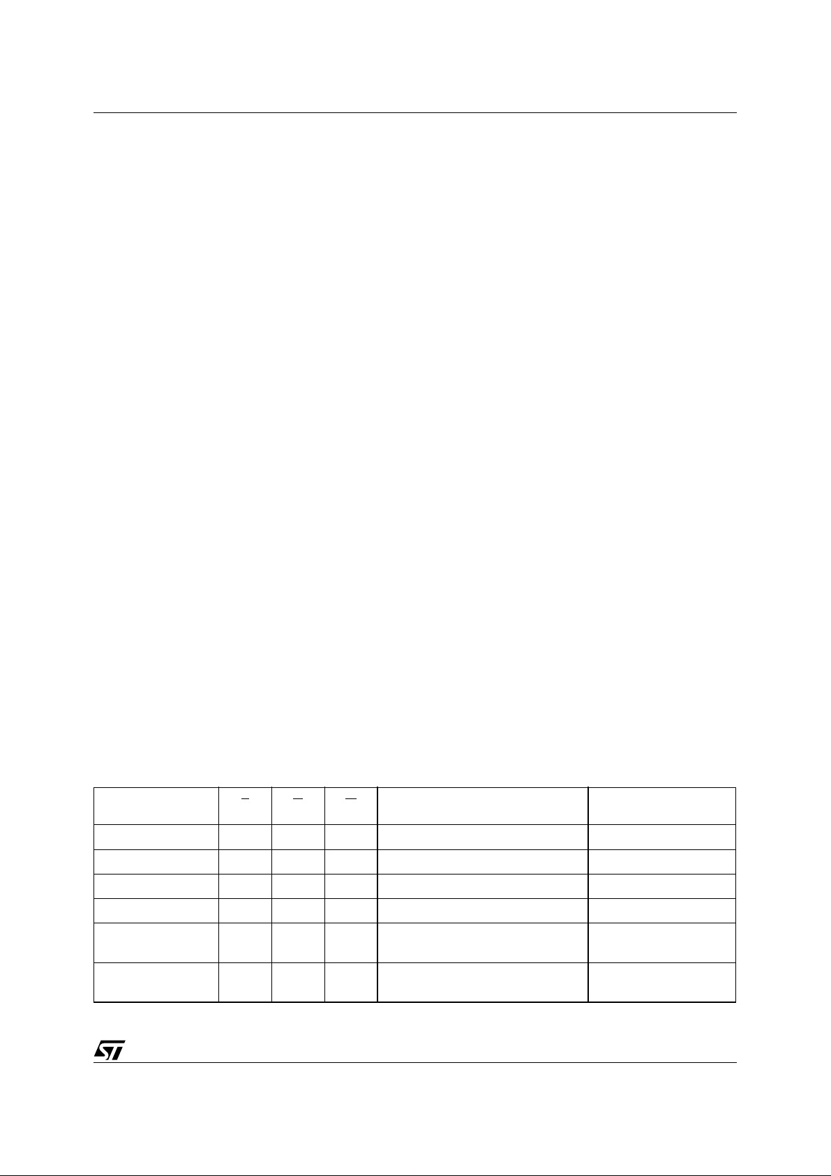
Parameter Min
Typ
(1)
Chip Erase 12 12 60 s
Block Erase (64 Kbytes) 0.8 6 s
Program (Byte) 10 200 µs
Chip Program (Byte by Byte) 12 60 s
Program/Erase Cycles (per Block) 100,000 cycles
Note: 1. TA = 25°C, VCC = 5V.
Typical after
100k W/E Cycles
(1)
Max Unit
13/37
Page 14

M29F080D
STATUS REGISTER
Bus Read operations from any address always
read the Status Register during Program and
Erase operations. It is also read during Erase Suspend when an address within a block being erased
is accessed.
The bits in the Status R egi st er are s umm ar iz ed in
Table 5, Status Register Bits.
Data Polling Bit (DQ7). The Data Polling Bit can be used to identify whether the Program/Erase Controller has successfully completed its operation or if it has respond ed to an Erase Suspend. The Data Polling Bit is output on DQ7 whe n the Status Register is read.
During Program operations the Data Polling Bit
outputs the complement of the bit being programmed to DQ7. After successful completion of
the Program operation the memory returns to
Read mode and Bus Read operations from the address just programm ed output DQ7, not its complement.
During Erase operations the Data Polli ng Bit outputs ’0’, the complement of the erased state of
DQ7. After su ccess ful co mpl etion of t he Er ase o peration the memory returns to Read Mode.
In Erase Suspend mode the Data Polli ng Bit will
output a ’1’ during a Bus Rea d operation withi n a
block being erased. The Data Polling Bit will
change from a ’0’ to a ’1’ when the Program/Erase
Controller has suspended the Erase operation.
Figure 6, Data Polling Flowc hart, gives an exam ple of how to use the Data Po lling Bit. A Valid Address is the address being programmed or an
address within the block being erased.
Toggle Bit (DQ6). The Toggle Bit can be used to identify whether the Program/Erase Controller has successfully completed its operation or if it has responded to an Erase Suspend. The To ggle Bit is output on DQ6 when the Status Register is read.
During Program and Er ase oper ations the Togg le
Bit changes from ’0’ to ’1 ’ to ’0’, etc., with succes sive Bus Read operations at any address. After
successful completion of the operation the memory returns to Read mode.
During Erase Suspend mode the Toggle Bit will
output when addressing a cell within a block being
erased. The Toggle Bit will stop toggling when the
Program/Erase Controller has suspended the
Erase operation.
If any attempt is made to era se a protec te d bl oc k,
the operation is aborted, no er ror is signalled and
DQ6 toggles for approximately 100µs. If any attempt is made to program a protected blo ck or a
suspended block, the operatio n is abor ted, no er-
ror is signalled and DQ6 toggles for approximately
1µs.
Figure 7, Data To ggle Flowchart, gives an example of how to use the Data Toggle Bit.
Error Bit (DQ5). The Error Bit can be used to identify errors detected by the Program/Erase Controller. The Error Bit is set to ’1’ when a Program, Block Erase or Chip Erase operation fails to write the correct data to the memory. If the Error Bit is set a Read/Reset command mus t be issu ed before other comma nds are issued. The Error bit is output on DQ5 when the Status Register is read.
Note that the Program command cannot change a
bit set to ’0’ back to ’1’ and attempting to do so will
set DQ5 to ‘1’. A Bus Read ope ration to that address will show the bi t is st ill ‘0 ’. On e of the Er as e
commands must be used to set all the bits in a
block or in the whole memory from ’0’ to ’1’.
Erase Timer Bi t (DQ3). The Eras e Timer Bit can be used to identify the start of Program/Erase Controller operation during a Block Erase command. Once the Program/Erase Controller starts erasing the Erase Timer Bit is set to ’1’. Before the Program/Erase Cont roller starts the Erase Timer Bit is set to ’0’ and additiona l blocks t o be erased may be written to the Command Interface. The Erase Timer Bit is output on DQ3 when the Status Register is read.
Alternative Toggle Bit (DQ2). The Alternative Toggle Bit can be u sed to monitor the Program/ Erase controller d uring Eras e operations. The Alternative Toggle Bit is output on DQ2 when the Status Register is read.
During Chip Erase and Block Erase operations the
Toggle Bit changes from ’0 ’ to ’1’ to ’0’, etc., wi th
successive Bus Rea d operations from ad dresses
within the blocks being eras ed. A protected bl ock
is treated the sam e as a block no t being erased.
Once the operation completes the memory returns
to Read mode.
During Erase Suspend the Alternative Toggle Bit
changes from ’0’ to ’1’ to ’0’, etc. with successive
Bus Read operations from addresses within the
blocks being erased . Bus Read operations to addresses within blocks not b ei ng e rase d wi ll output
the memory cell data as if in Read mode.
After an Erase o per at ion th at ca us es th e Er ror B it
to be set the Alternative Toggle Bit can be used to
identify which block or blocks have caused the error. The Alternative Toggle Bit changes from ’0’ to
’1’ to ’0’, etc. with successive Bus Read Operations from addresses with in blocks that have not
erased correctly. Th e Alternative Toggle B it does
not change if the addressed block has erased correctly.
14/37
Page 15

M29F080D
Table 5. Status Register Bits
Operation Address DQ7 DQ6 DQ5 DQ3 DQ2
Program Any Address DQ7 Toggle 0 – – 0
Program During Erase
Suspend
Any Address DQ7
Program Error Any Address DQ7
Chip Erase Any Address 0 Toggle 0 1 Toggle 0
Block Erase before
timeout
Erasing Block 0 Toggle 0 0 Toggle 0
Non-Erasing Block 0 Toggle 0 0 No Toggle 0
Erasing Block 0 Toggle 0 1 Toggle 0
Block Erase
Non-Erasing Block 0 Toggle 0 1 No Toggle 0
Erasing Block 1 No Toggle 0 – Toggle 1
Erase Suspend
Non-Erasing Block Data read as normal 1
Good Block Address 0 Toggle 1 1 No Toggle 0
Erase Error
Faulty Block Address 0 Toggle 1 1 Toggle 0
Note: Unspecified data bits should be ignored.
Toggle 0 – – 0
Toggle 1 – – 0
RB
Figure 6. Data Polling Flowchart Figure 7. Data Toggle Flowchart
DQ5 & DQ6
READ DQ6
NO
READ DQ6
START
READ
DQ6
=
TOGGLE
YES
DQ5
= 1
YES
TWICE
DQ6
=
TOGGLE
YES
NO
NO
START
READ DQ5 & DQ7
at VALID ADDRESS
DQ7
YES
=
DATA
NO
NO
DQ5
= 1
YES
READ DQ7
at VALID ADDRESS
DQ7
YES
=
DATA
NO
FAIL PASS
AI05278
FAIL PASS
AI05279
15/37
Page 16

M29F080D
MAXIMUM RATING
Stressing the device above the ra ting l isted in the
Absolute Maximum Ratin gs table ma y cause per manent damage to the device. Expos ure to Ab so lute Maximum Rating conditions for extended
periods may affect device reliability. These are
stress ratings only and operation of th e device at
Table 6. Absolute Maximum Ratings
Symbol Parameter Min Max Unit
T
BIAS
T
STG
V
IO
V
CC
V
ID
Note: 1. Minimum Voltage may undershoot to –2V or overshoot to VCC +2V during transition for a maximum of 20ns.
Temperature Under Bias –50 125 °C
Storage Temperature
Input or Output Voltage
Supply Voltage –0.6 6 V
Identification Voltage –0.6 13.5 V
(1)
these or any other conditions above those indicated in the Operating sections of this specification is
not implied. Refer also to the STMicroelectronics
SURE Program and o ther relevant quality documents.
–65 150 °C
V
–0.6
CC
+ 0.6
V
16/37
Page 17

M29F080D
DC AND AC PARAMETERS
This section summ arizes the operating measurement conditions, and th e DC and AC c haracteris tics of the device. The parameters in the DC and
AC characteristics Tables that follow, are derived
from tests performed under the Measurement
Table 7. Operating and AC Measurement Conditions
Parameter
Min Max Min Max
V
Supply Voltage
CC
Ambient Operating Temperature – 40 85 – 40 85 °C
Load Capacitance (CL)
Input Rise and Fall Times 10 10 ns
Input Pulse Voltages 0 to 3 0.45 to 2.4 V
Input and Output Timing Ref. Voltages 1.5 0.8 and 2.0 V
4.5 5.5 4.5 5.5 V
Conditions summarized in Table 7, Operating and
AC Measurement Conditions. Designers should
check that the oper ating conditi ons in thei r circuit
match the operating conditions when relying on
the quoted parameters.
M29F080D
30 100 pF
Unit55 70/ 90
Figure 8. AC Measurement I/O Waveform Figure 9. AC Measurement Load Circuit
1.3V
High Speed (55ns)
V
3V
0V
Standard (70, 90ns)
2.4V
0.45V
1.5V
2.0V
0.8V
AI05276
CC
DEVICE
UNDER
TEST
0.1µF
CL includes JIG capacitance
1N914
3.3kΩ
CL
Table 8. Device Capacitance
Symbol Parameter Test Condition Min Max Unit
C
IN
C
OUT
Note: Sampled only, not 100% tested.
Input Capacitanc e
Output Capacitance
V
V
OUT
IN
= 0V
= 0V
6pF
12 pF
OUT
AI05277
17/37
Page 18

M29F080D
Table 9. DC Characteristics
Symbol Parameter Test Condition Min Max Unit
I
I
CC1
I
CC2
I
CC3
I
LO
Input Leakage Current
LI
Output Leakage Current
Supply Current (Read)
Supply Current (Standby) TTL
Supply Current (Standby) CMOS
0V ≤ V
≤ V
IN
CC
0V ≤ V
= VIL, G = VIH, f = 6MHz
E
E
= VCC ± 0.2V,
RP
≤ V
OUT
CC
E
= V
IH
= VCC ±0.2V
±1 µA
±1 µA
20 mA
2mA
150 µA
(1)
Supply Current (Program/Erase)
I
CC4
V
V
V
Input Low Voltage –0.5 0.8 V
IL
Input High Voltage 2
IH
Output Low Voltage
OL
Output High Voltage TTL
V
OH
V
I
ID
V
LKO
Note: 1. Sampled only, not 100% tested.
Output High Voltage CMOS
Identification Voltage 11.5 12.5 V
ID
Identification Current
Program/Erase Lockout Supply
(1)
Voltage
Program/Erase
Controller active
I
= 5.8mA
OL
I
= –2.5mA
OH
= –100µA VCC – 0.4
I
OH
A9 = V
ID
20 mA
V
+ 0.5
CC
0.45 V
2.4 V
100 µA
3.2 4.2 V
V
V
18/37
Page 19

Figure 10. Read AC Waveforms
M29F080D
tAVAV
A0-A19
tAVQV tAXQX
E
tELQV
tELQX tEHQZ
G
tGLQX tGHQX
DQ0-DQ7
VALID
tGLQV
Table 10. Read AC Characteristics
Symbol Alt Parameter Test Condition
E
t
AVAV
t
AVQV
t
ELQX
t
ELQV
t
GLQX
t
GLQV
t
EHQZ
t
GHQZ
t
EHQX
t
GHQX
t
AXQX
Note: 1. Sampled only, not 100% tested.
t
Address Valid to Next Address Valid
RC
t
Address Valid to Output Valid
ACC
(1)
t
(1)
(1)
(1)
Chip Enable Low to Output Transition
LZ
t
Chip Enable Low to Output Valid
CE
t
Output Enable Low to Output Transition
OLZ
t
Output Enable Low to Output Valid
OE
t
Chip Enable High to Ou tput Hi-Z
HZ
t
Output Enable High to Output Hi-Z
DF
Chip Enable, Output Enable or Address
t
OH
Transition to Output Transition
= VIL,
G
= V
E
= VIL,
G
= V
G
= V
G
= V
E
= V
E
= V
G
= V
E
= V
IL
IL
IL
IL
IL
IL
IL
IL
tEHQX
tGHQZ
VALID
AI06145
M29F080D
Unit
55 70/ 90
Min 55 70 ns
Max 55 70 ns
Min 0 0 ns
Max 55 70 ns
Min 0 0 ns
Max 30 30 ns
Max 18 20 ns
Max 18 20 ns
Min 0 0 ns
19/37
Page 20

M29F080D
Figure 11. Write AC Waveforms, Write Enable Controlled
tAVAV
A0-A19
tAVWL
E
VALID
tWLAX
tWHEH
tELWL
G
tWLWHtGHWL
W
tDVWH
DQ0-DQ7
V
CC
RB
tVCHEL
VALID
tWHRL
Table 11. Write AC Characteristics, Write Enable Controlled
Symbol Alt Parameter
t
AVAV
t
ELWL
t
WLWH
t
DVWH
t
WHDX
t
WHEH
t
WHWL
t
AVWL
t
WLAX
t
GHWL
t
WHGL
t
WHRL
t
VCHEL
Note: 1. Sampled only, not 100% tested.
(1)
t
WC
t
CS
t
WP
t
DS
t
DH
t
CH
t
WPH
t
AS
t
AH
t
OEH
t
BUSY
t
VCSVCC
Address Valid to Next Address Valid Min 55 70 ns
Chip Enable Low to Write Enable Low Min 0 0 ns
Write Enable Low to Write Enable High Min 45 45 ns
Input Valid to Write Enable High Min 45 45 ns
Write Enable High to Input Transition Min 0 0 ns
Write Enable High to Chip Enable High Min 0 0 ns
Write Enable High to Write Enable Low Min 20 20 ns
Address Valid to Write Enable Low Min 0 0 ns
Write Enable Low to Address Transition Min 45 45 ns
Output Enable High to Write Enable Low Min 0 0 ns
Write Enable High to Output Enable Low Min 0 0 ns
Program/Erase Valid to RB Low Max 30 30 ns
High to Chip Enable Low
Min 50 50 µs
tWHGL
tWHWL
tWHDX
AI06146
M29F080D
Unit
55 70/ 90
20/37
Page 21

Figure 12. Write AC Waveforms, Chip Enable Controlled
tAVAV
A0-A19
tAVEL
W
VALID
M29F080D
tELAX
tEHWH
tWLEL
G
tELEHtGHEL
E
tDVEH
DQ0-DQ7
V
CC
RB
tVCHWL
VALID
tEHRL
Table 12. Write AC Characteristics, Chip Enable Controlled
Symbol Alt Parameter
t
AVAV
t
WLEL
t
ELEH
t
DVEH
t
EHDX
t
EHWH
t
EHEL
t
AVEL
t
ELAX
t
GHEL
t
EHGL
(1)
t
EHRL
t
VCHWL
Note: 1. Sampled only, not 100% tested.
t
WC
t
WS
t
CP
t
DS
t
DH
t
WH
t
CPH
t
AS
t
AH
t
OEH
t
BUSY
t
VCSVCC
Address Valid to Next Address Valid Min 55 70 ns
Write Enable Low to Chip Enable Low Min 0 0 ns
Chip Enable Low to Chip Enable High Min 45 45 ns
Input Valid to Chip Enable High Min 45 45 ns
Chip Enable High to Input Transition M in 0 0 ns
Chip Enable High to Write En able High Min 0 0 n s
Chip Enable High to Chip Enable Low Min 20 20 ns
Address Valid to Chip Enable Low Min 0 0 ns
Chip Enable Low to Address Transition Min 45 45 ns
Output Enable High Chip Enable Low Min 0 0 ns
Chip Enable High to Output Enable Low Min 0 0 ns
Program/Erase Valid to RB Low Max 30 30 ns
High to Write Enable Low
Min 50 50 µs
tEHGL
tEHEL
tEHDX
AI06147
M29F080D
Unit
55 70/ 90
21/37
Page 22

M29F080D
Figure 13. Reset/Block Temporary Unprotect AC Waveforms
E, G
W,
tPHWL, tPHEL, tPHGL
RB
RP
Table 13. Reset/Block Temporary Unprotect AC Characteristics
Symbol Alt Parameter
(1)
t
PHWL
t
PHEL
(1)
t
PHGL
(1)
t
RHWL
(1)
t
RHEL
(1)
t
RHGL
t
PLPX
(1)
t
t
PLYH
t
PHPHH
Note: 1. Sampled only, not 100% tested.
(1)
READY
t
RP High to Write Enable Low, Chip Enable Low,
t
RH
Output Enable Low
RB High to Write Enable Low, Chip Enable Low,
t
RB
Output Enable Low
t
RP Pulse Width Min 500 500 ns
RP
RP Low to Read Mode Max 10 10 µs
RP Rise Time to V
VIDR
tPLPX
ID
tPLYH
Min 50 50 ns
Min 0 0 ns
Min 500 500 ns
tRHWL, tRHEL, tRHGL
tPHPHH
AI02931B
M29F080D
Unit
55 70/ 90
22/37
Page 23

PACKAGE MECHANICAL
TSOP40 – 40 lead Plastic Thin Small Outline, 10 x 20mm, Package Outline
A2
M29F080D
Note: Drawing is not to scale.
1 N
N/2
TSOP-a
D1
DIE
E
A
D
C
e
B
CP
LA1 α
TSOP40 – 40 lead Plastic Thin Small Outline, 10 x 20mm, Package Mechanical Data
Symbol
Typ Min Max Typ Min Max
A 1.200 0.0472
A1 0.050 0.150 0.0020 0.0059
A2 0.950 1.050 0.0374 0.0413
B 0.170 0.270 0.0067 0.0106
C 0.100 0.210 0.0039 0.0083
D 19.800 20.200 0.7795 0.7953
D1 18.300 18.500 0.7205 0.7283
E 9.900 10.100 0.3898 0.3976
e 0.500 – – 0.0197 – –
L 0.500 0.700 0.0197 0.0276
α 0° 5° 0° 5°
N40 40
CP 0.100 0.0039
millimeters inches
23/37
Page 24

M29F080D
SO44 – 44 lead Plastic Small Outline, 525 mils body width, Package Outline
A
C
LA1 α
SO-d
Note: Drawing is not to scale.
A2
b
e
D
N
1
CP
E
EH
SO44 – 44 lead Plastic Small Outline, 525 mils body width, Package Mechanical Data
Symbol
Typ Min Max Typ Min Max
A2.800.1102
A1 0.10 0.0039
A2 2.30 2.20 2.40 0.0906 0.0866 0.0945
b 0.40 0.35 0.50 0.0157 0.0138 0.0197
C 0.15 0.10 0.20 0.0059 0.0039 0.0079
CP 0.08 0.0030
E 13.30 13.20 13.50 0.5236 0.5197 0.5315
D 28.20 28.00 28.40 1.1102 1.1024 1.1181
e 1.27 – – 0.0500 – –
HE 16.00 15.75 16.25 0.6299 0.6201 0.6398
L 0.80 0.0315
N44 44
α 88
millimeters inches
24/37
Page 25

PART NUMBERING
Table 14. Ordering Information Scheme
Example: M29F080D 55 N 1 T
Device Type
M29
Operating Voltage
F = V
Device Function
080D = 8 Mbit (1Mb x8), Uniform Block
Speed
55 = 55 ns
70 = 70 ns
90 = 90 ns
Package
N = TSOP40: 10 x 20 mm
M = SO44
= 5V ± 10%
CC
M29F080D
Temperature Range
1 = 0 to 70 °C
6 = –40 to 85 °C
Option
Blank = Standard Packing
T = Tape & Reel Packing
E = ECOPACK Package, Standard Packing
F = ECOPACK Package, Tape & Reel Packing
Devices are shipped from the factory with the memory content bits erased to ’1’.
For a list of availa ble opt ion s (Spe ed, Pac k age , et c... ) or for fu r ther i nfo rm ati on o n a ny aspec t o f th is de vice, please contact the ST Sales Office nearest to you.
25/37
Page 26

M29F080D
APPENDIX A. BLOCK ADDRESS TABLE
Table 15. Block Addresses, M29F080D
Size,
#
KByte
15 64 0F0000h-0FFFFFh
14 64 0E0000h-0EFFFFh
13 64 0D0000h-0DFFFFh
12 64 0C0000h-0CFFFFh
11 64 0B0000h-0BFFFFh
10 64 0A0000h-0AFFFFh
9 64 090000h-09FFFFh
8 64 080000h-08FFFFh
7 64 070000h-07FFFFh
6 64 060000h-06FFFFh
5 64 050000h-05FFFFh
4 64 040000h-04FFFFh
3 64 030000h-03FFFFh
2 64 020000h-02FFFFh
1 64 010000h-01FFFFh
0 64 000000h-00FFFFh
Address Range Protection Group
3
2
1
0
26/37
Page 27

APPENDIX B. COMMON FLASH INTERFACE (CFI)
The Common Flash Interface is a JEDEC approved, standardized data structure that can be
read from the Flash memory device. It allows a
system software to query the de vice to de termine
various electrical a nd timing parameters, density
information and functions su pported by the mem ory. The system can interface easily with the device, enabling the so ftwar e to u pgr ade it se lf wh en
necessary.
When the CFI Query Command is issued th e de-
is read from the memory. Tables 16, 17, 18, 19, 20
and 21 show the addresses us ed to retrieve the
data.
The CFI data structure also contains a security
area where a 64 bit unique security number is written (see Table 21, Security Code area). Thi s area
can be accessed onl y in Read mode by the final
user. It is imposs ible to chang e the secur ity num ber after it has been written b y ST. Issu e a Read
command to return to Read mode.
vice enters CFI Query mode and the data structure
Table 16. Query Structure Overview
Address Sub-section Name Description
10h CFI Query Identification String Command set ID and algorithm data offset
1Bh System Interface Information Device timing & voltage information
27h Device Geometry Definition Flash device layout
40h
61h Security Code Area 64 bit unique device number
Note: Query data are always presented on the lowest order data outputs.
Primary Algorithm-specific Extended Query
table
Additional informatio n spe ci fic to the Pr im ary
Algorithm (optio na l)
M29F080D
Table 17. CFI Query Identification String
Address Data Description Value
10h 51h "Q"
11h 52h Query Unique ASCII String "QRY" "R"
12h 59h "Y"
13h 02h
14h 00h
15h 40h
16h 00h
17h 00h
18h 00h
19h 00h
1Ah 00h
Primary Algorithm Co mma n d Set an d Co nt r ol In t er face ID code 16 bit ID code
defining a specific algorithm
Address for Primary Algorithm extended Query table (see Table 19) P = 40h
Alternate Vendor Command Set and Control Interface ID Code second vendor
- specified algorithm supported
Address for Alternate Algorithm extended Query table
AMD
Compatible
NA
NA
27/37
Page 28

M29F080D
Table 18. CFI Query System Interface Information
Address Data Description Value
V
Logic Supply Minimum Program/Erase voltage
1Bh 45h
1Ch 55h
1Dh 00h
1Eh 00h
1Fh 04h
20h 00h
21h 0Ah
22h 00h
23h 04h
24h 00h
25h 03h
26h 00h
Note: 1. Not supported in the CFI
CC
bit 7 to 4 BCD value in volts
bit 3 to 0 BCD value in 100 mV
Logic Supply Maximum Program/Erase voltage
V
CC
bit 7 to 4 BCD value in volts
bit 3 to 0 BCD value in 100 mV
V
[Programming] Supply Minimum Program/Erase voltage
PP
00h not supported
[Programming] Supply Maximum Program/Erase voltage
V
PP
00h not supported
Typical timeout per single byte program = 2
n
µs
Typical timeout for minimum size write buffer program = 2
Typical tim eo ut pe r indiv idu al block erase = 2
Typical tim eo ut for full chip erase = 2
n
Maximum timeout for byte program = 2
Maximum timeout for write buffer program = 2
Maximum timeout per individual block erase = 2
Maximum timeout for chip erase = 2
n
times typical
n
ms
ms
n
times typical
n
times typical
n
times typical
n
µs
see note (1)
256µs
see note (1)
4.5V
5.5V
NA
NA
16µs
NA
1s
NA
8s
28/37
Page 29

M29F080D
Table 19. Device Geometry Definition
Address Data Description Value
27h 14h
28h
29h
2Ah
2Bh
2Ch 01h
2Dh
2Eh
2Fh
30h
00h
00h
00h
00h
0Fh
00h
00h
01h
Device Size = 2
Flash Device Interface Code description
Maximum number of bytes in multi-byte program or page = 2
Number of Erase Block Regions within the device.
It specifies the number of regio n s within the device containing contiguous
Erase Blocks of the same size.
Region 1 Information
Number of identical size erase block = 000Fh+1
Region 1 Information
Block size in Region 1 = 0100h * 256 byte
n
in number of bytes
1 MByte
x8 only
Async.
n
64 Kbyte
NA
1
16
29/37
Page 30

M29F080D
Table 20. Primary Algorithm-Specific Extended Query Table
Address Data Description Value
40h 50h
41h 52h "R"
42h 49h "I"
43h 31h Major version number, ASCII "1"
44h 30h Minor version number, ASCII "0"
45h 00h Address Sensitive Unlock (bits 1 to 0)
46h 02h Erase Suspend
47h 04h Block Protection
48h 01h Temporary Block Unprotect
49h 04h Block Protect /Unprotect
4Ah 00h Simultaneous Operations, 00 = not supported No
4Bh 00h Burst Mode, 00 = not supported, 01 = supported No
4Ch 00h Page Mode, 00 = not supported, 01 = 4 page word, 02 = 8 page word No
Primary Algorithm extended Query table unique ASCII string “PRI”
00 = required, 01= not required
Silicon Revision Number (bits 7 to 2)
00 = not supported, 01 = Read only, 02 = Read and Write
00 = not supported, x = number of blocks per group
00 = not supported, 01 = supported
04 = M29W400B mode
"P"
Yes
2
4
yes
4
Table 21. Security Code Area
Address Data Description
61h XX
62h XX
63h XX
64h XX
65h XX
66h XX
67h XX
68h XX
64 bit: unique device number
30/37
Page 31

APPENDIX C. BLOCK PROTECTION
Block protection can be used to prevent any operation from modifying the data stored in the memory. The blocks are protected in groups, refer to
Appendix A, Table 15 for detai ls of the Protecti on
Groups. Once protected, Program and Er ase operations within the pr otected group fail to change
the data.
There are three techniques that can be used to
control Block Pro tection, these are the Programmer technique, the In-System technique and Temporary Unprotection. Temporary Unprotection is
controlled by the Reset/Block Temporary Unprotection pin, RP
; this is described in the Si gna l De -
scriptions section.
To protect the Extended Block issue the Enter Ex-
tended Block command and then use either the
Programmer or In-System technique. Once protected issue the Exit Extended Bl oc k co mma nd to
return to read mode. The Exte nded Block pro tection is irreversible , once protected the protection
cannot be undone.
Programmer Technique
The Programmer techniqu e uses high (V
) volt-
ID
age levels on some of the bus pins. These cannot
be achieved using a standard microprocessor bus,
therefore the technique is re commended only for
use in Programming Equipment.
To protect a group of blocks follow the flowchart in
Figure 14, Programme r Equipment Block Pr otect
Flowchart. To unprotect the whole chip it is necessary to protect all of the groups first, then all
groups can be unpr otected at the same time . To
unprotect the chip fo llow Figure 15, Programmer
Equipment Chip Unprotect Flowchart. Table 22,
M29F080D
Programmer Techn ique Bus Operations, gives a
summary of each operation.
The timing on these flowcharts is critical. Care
should be taken to ensure th at, where a paus e is
specified, it is followe d as closely as possible. Do
not abort the procedure befor e reaching the end.
Chip Unprotect can take several seconds and a
user message should be provided to show that the
operation is progressing.
In-System Technique
The In-System technique r equires a high voltage
level on the Reset/Blocks Temporary Unprotect
pin, RP
maximum ratings of the components on the microprocessor bus, therefore this technique is suitable
for use after the memory has been fitted to the system.
To protect a group of blocks follow the flowchart in
Figure 16, In-System Block Protect Flowc hart. To
unprotect the whole chip it is necessary to prote ct
all of the groups first, then al l the groups can be
unprotected at the same time. To unprotect the
chip follow Figure 17, In-System Chip Unprotect
Flowchart.
The timing on these flowcharts is critical. Care
should be taken to ensure th at, where a paus e is
specified, it is followe d as closely as possible. Do
not allow the microproce ssor to servi ce interrupts
that will upset the timing and do not abort the procedure before reaching the end. Chip Unprotect
can take several seconds and a user message
should be provided to show that the operation is
progressing.
. This can be achieved without violating the
Table 22. Programmer Technique Bus Operations, BYTE
Operation E G W
Block (Group)
(1)
Protect
Chip Unprotect
Block (Group)
Protection Verify
Block (Group)
Unprotection Verify
Note: 1. Block Protection Groups are shown in Appendix A, Table 15.
VILVIDVIL Pulse
V
IDVIDVIL
V
V
IL
VILV
Pulse
V
IL
IL
IH
V
IH
A9 = V
A0 = VIL, A1 = VIH, A6 = VIL, A9 = VID,
A0 = VIL, A1 =VIH, A6 = VIH, A9 = VID,
Address Inputs
A0-A19
, A12-A19 Block Address
ID
Others = X
A9 = V
, A12 = VIH, A15 = VIH
ID
Others = X
A12-A19 Block Address
Others = X
A12-A19 Block Address
Others = X
= VIH or V
IL
Data Inputs/Outputs
DQ15A–1, DQ14-DQ0
X
X
Pass = XX01h
Retry = XX00h
Retry = XX01h
Pass = XX00h
31/37
Page 32

M29F080D
Figure 14. Programmer Equipment Group Protect Flowchart
START
ADDRESS = GROUP ADDRESS
W = V
IH
n = 0
G, A9 = VID,
E = V
IL
Wait 4µs
W = V
IL
Wait 100µs
W = V
IH
Verify Protect Set-upEnd
E, G = VIH,
A0, A6 = VIL,
A1 = V
IH
E = V
IL
Wait 4µs
G = V
IL
Wait 60ns
Read DATA
DATA
=
01h
YES
A9 = V
IH
E, G = V
IH
PASS
NO
++n
= 25
A9 = V
E, G = V
NO
YES
IH
IH
Note: Block Protection Groups are shown in Append ix A, Ta ble 15.
32/37
FAIL
AI05574
Page 33

Figure 15. Programmer Equipment Chip Unprotect Flowchart
START
PROTECT ALL GROUPS
M29F080D
CURRENT GROUP = 0
ADDRESS = CURRENT GROUP ADDRESS
A0 = VIL, A1, A6 = V
n = 0
A6, A12, A15 = V
E, G, A9 = V
Wait 4µs
W = V
IL
Wait 10ms
W = V
IH
E, G = V
IH
E = V
IL
Wait 4µs
(1)
IH
ID
IH
G = V
Wait 60ns
Verify Unprotect Set-upEnd
++n
NO
= 1000
YES
A9 = V
IH
E, G = V
IH
FAIL PASS
Note: Block Protection Groups are shown in Append ix A, Ta ble 15.
Read DATA
DATA
=
00h
IL
YESNO
A9 = V
E, G = V
INCREMENT
CURRENT GROUP
LAST
GROUP
NO
YES
IH
IH
AI05575
33/37
Page 34

M29F080D
Figure 16. In-System Equipment Group Protect Flowchart
START
n = 0
RP = V
ID
Verify Protect Set-upEnd
ADDRESS = GROUP ADDRESS
ADDRESS = GROUP ADDRESS
ADDRESS = GROUP ADDRESS
ADDRESS = GROUP ADDRESS
A0 = VIL, A1 = VIH, A6 = V
WRITE 60h
A0 = VIL, A1 = VIH, A6 = V
WRITE 60h
A0 = VIL, A1 = VIH, A6 = V
Wait 100µs
WRITE 40h
A0 = VIL, A1 = VIH, A6 = V
Wait 4µs
READ DATA
DATA
RP = V
=
01h
NO
YES
IH
IL
IL
IL
IL
++n
= 25
NO
ISSUE READ/RESET
COMMAND
PASS
Note: Block Protection Groups are shown in Append ix A, Ta ble 15.
34/37
YES
RP = V
IH
ISSUE READ/RESET
COMMAND
FAIL
AI05576
Page 35

Figure 17. In-System Equipment Chip Unprotect Flowchart
START
PROTECT ALL GROUPS
M29F080D
Verify Unprotect Set-upEnd
CURRENT GROUP = 0
A0 = VIL, A1 = VIH, A6 = V
A0 = VIL, A1 = VIH, A6 = V
ADDRESS = CURRENT GROUP ADDRESS
A0 = VIL, A1 = VIH, A6 = V
ADDRESS = CURRENT GROUP ADDRESS
A0 = VIL, A1 = VIH, A6 = V
n = 0
RP = V
ID
WRITE 60h
ANY ADDRESS WITH
WRITE 60h
ANY ADDRESS WITH
Wait 10ms
WRITE 40h
Wait 4µs
READ DATA
IH
IH
IH
IH
INCREMENT
CURRENT GROUP
++n
NO
= 1000
YES
RP = V
IH
ISSUE READ/RESET
COMMAND
FAIL
Note: Block Protection Groups are shown in Append ix A, Ta ble 15.
DATA
=
00h
YESNO
LAST
GROUP
RP = V
ISSUE READ/RESET
COMMAND
PASS
NO
YES
IH
AI05577
35/37
Page 36

M29F080D
REVISION HISTORY
Table 23. Document Revision History
Date Version Revision Details
03-Dec-2001 -01 First Issue
Description of Re ad y/B us y sign al cla r ifi ed (and Fig ur e 13 mo difi ed )
05-Apr-2002 -02
19-Sep-2005 3.0
Clarified allowable commands during block erase
Clarified the mode the device returns to in the CFI Read Query command section
Table 14. Ordering Information Scheme: standard package added and ECOP A CK version
added for both standard package and Tape & Reel packing.
Datasheet status changed to FULL DATASHEET.
36/37
Page 37

M29F080D
Information furnished is be lieved to be a ccur ate and reli able. Howe ver, STMicroele ctronic s assu mes no r esponsib ilit y for th e consequences
of use of such information nor for any infrin gement of patent s or other rights of third parties which ma y result from it s use. No license is granted
by implication or otherwi se under any patent or patent rights of STMicroelectronics. Specifications mentioned in this publication are subject
to change without not ice. This pub licat ion su persed es and repl aces all in format ion previou sly su pplie d. STMicroele c tronic s prod ucts a re no t
authorized for use as critical compone nts in life support devices or systems without express written approval of STMicroelectronics.
The ST logo is a registered trademark of STMicroelectronics.
All other names are the property of their respective owners
© 2005 STMicroelectronics - All rights reserved
Australia - Belgium - Brazil - Canada - China - Czech Republic - Finland - France - Germany - Hong Kong - India - Israel - Italy - Japan -
Malaysia - Malta - Morocco - Singapore - Spain - Sweden - Switzerland - United Kingdom - United States of America
STMicroelectronics group of companies
www.st.com
37/37
 Loading...