

ST M29F040B User Manual
M29F040B
4 Mbit (512Kb x8, Uniform Block) Single Supply Flash Memory
PRELIMINARY DATA
■ SINGLE 5V ± 10% SUPPLY VOLTAGE for
PROGRAM, ERASE and READ OPERATIONS
■ ACCESS TIME: 45ns
■ PROGRAMMING TIME
–8µs per Byte typical
■ 8 UNIFORM 64 Kbytes MEMORY BLOCKS
■ PROGRAM/ERASE CONTROLLER
– Embedded Byte Program algorithm
– Embedded Multi-Block/Chip Erase algorithm
– Status Register Polling and Toggle Bits
■ ERASE SUSPEND and RESUME MODES
– Read and Program another Block during
Erase Suspend
■ UNLOCKBYPASS PROGRAM COMMAND
– Faster Production/Batch Programming
■ LOW POWER CONSUMPTION
– Standby andAutomatic Standby
■ 100,000 PROGRAM/ERASE CYCLES per
BLOCK
■ 20 YEARS DATA RETENTION
– Defectivity below 1 ppm/year
■ ELECTRONIC SIGNATURE
– Manufacturer Code: 20h
– Device Code: E2h
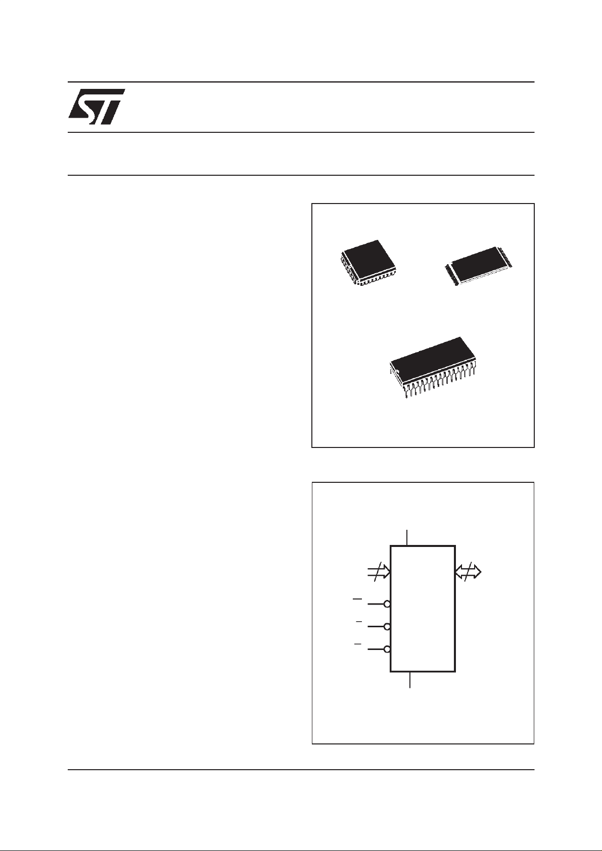
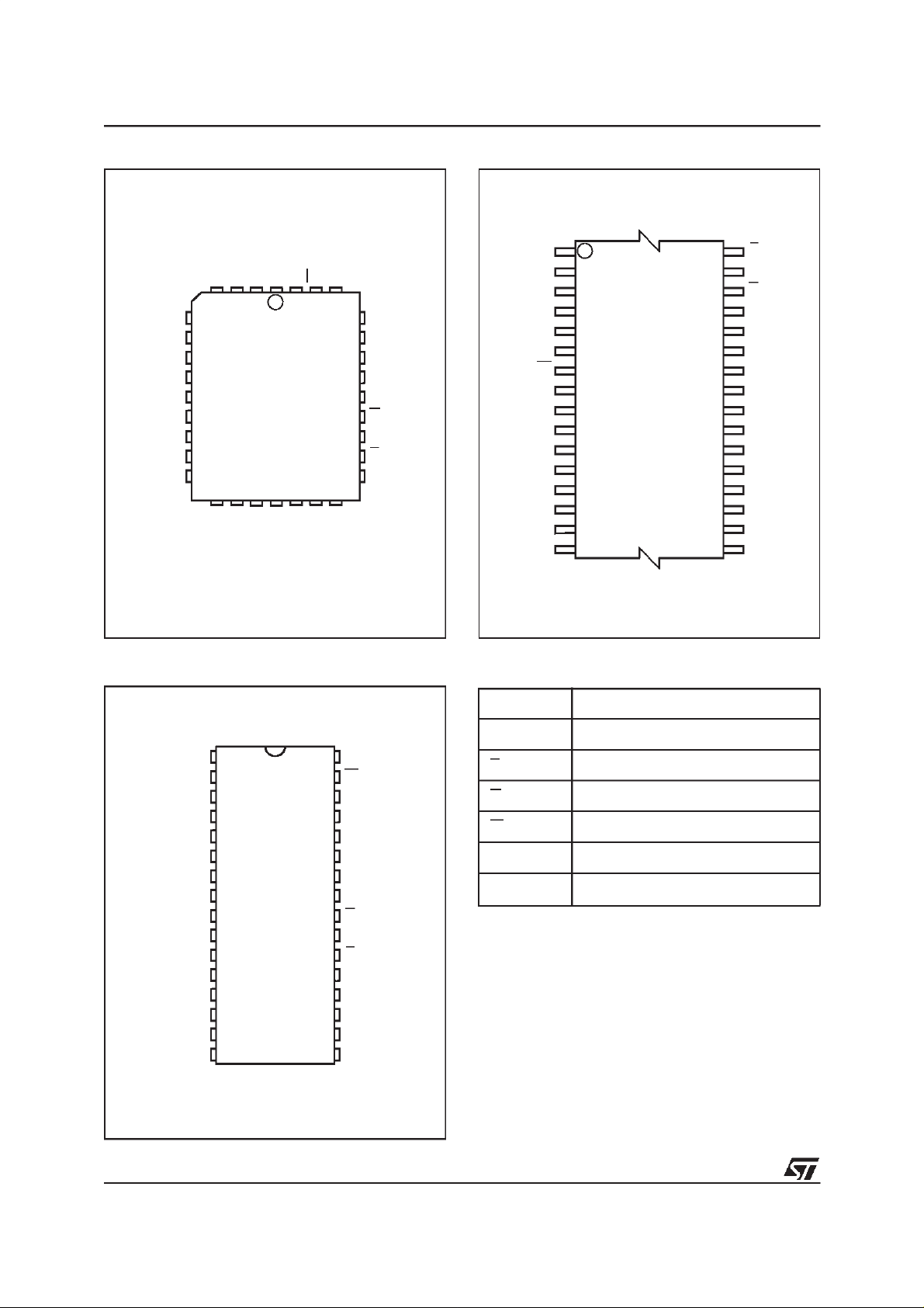
PLCC32 (K)
32
1
Figure 1. Logic Diagram
V
CC
19
A0-A18
PDIP32 (P)
TSOP32 (N)
8 x 20mm
8
DQ0-DQ7
W
E
G
September 1999
This is preliminary information on a new product now in development or undergoing evaluation. Details are subject to change without notice.
M29F040B
V
SS
AI02900
1/21
M29F040B
Figure 2A. PLCC Connections
CC
A16
A7
A6
A5
A4
A3
A2
A1
A0
DQ0
A12
9
DQ1
A18
A15
1
32
M29F040B
17
SS
V
DQ2
DQ3
V
DQ4
W
DQ5
A17
25
DQ6
A14
A13
A8
A9
A11
G
A10
E
DQ7
AI02901
Figure 2B. TSOP Connections
A11 G
A9
A8
A13
A14
A17
V
CC
A18
A16
A15
A12
A7
A6
A5
A4 A3
1
W
8
M29F040B
9
16 17
32
25
24
AI02902
A10
E
DQ7
DQ6
DQ5
DQ4
DQ3
V
SS
DQ2
DQ1
DQ0
A0
A1
A2
Figure 2C. PDIP Connections
A18 V
1
2
A15
3
A12
4
A7
5
A6
6
A5
7
A4
8
A3
A2
A1
A0
DQ0
DQ2
SS
M29F040B
9
10
11
12
13
14
15
16
AI02910
32
31
30
29
28
27
26
25
24
23
22
21
20
19
18
17
CC
WA16
A17
A14
A13
A8
A9
A11
G
A10
E
DQ7
DQ6
DQ5DQ1
DQ4
DQ3V
Table 1. Signal Names
A0-A18 Address Inputs
DQ0-DQ7 Data Inputs/Outputs
E Chip Enable
G Output Enable
W Write Enable
V
CC
V
SS
Supply Voltage
Ground
SUMMARY DESCRIPTION
The M29F040B is a 4Mbit (512Kb x8) non-volatile
memory that can be read, erased and reprogrammed. Theseoperations can be performedusing a single 5V supply. On power-up the memory
defaults to its Read mode where it can be read in
the same way as a ROM or EPROM. The
M29F040B is fully backward compatible with the
M29F040.
The memory is divided into blocks that can be
erased independently so it is possible to preserve
2/21
M29F040B
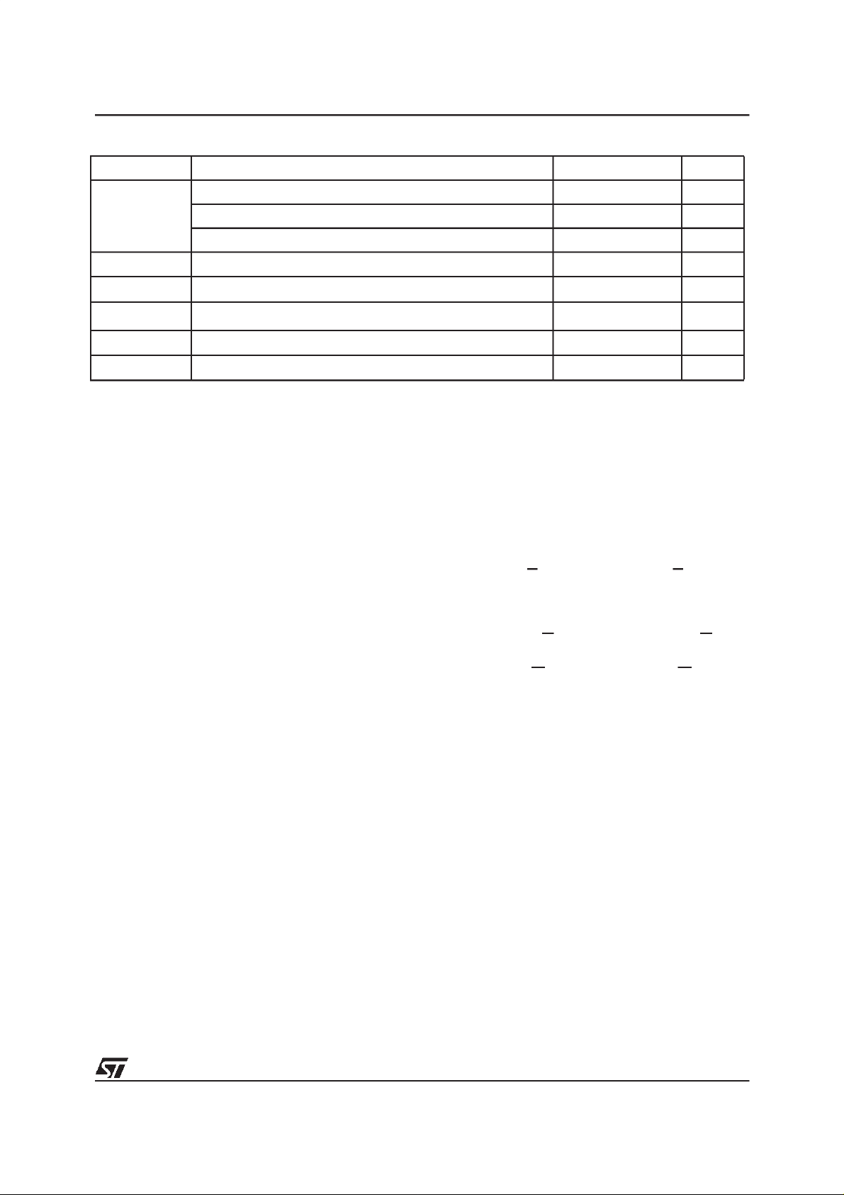
Table 2. Absolute Maximum Ratings
Symbol Parameter Value Unit
Ambient Operating Temperature (Temperature Range Option 1) 0 to 70 °C
T
A
T
BIAS
T
STG
(2)
V
IO
V
CC
V
ID
Note: 1. Except for the rating ”Operating Temperature Range”, stresses above those listed in the Table ”Absolute Maximum Ratings” may
cause permanent damage to the device. These are stress ratings only and operation of the device atthese or any other conditions
above those indicated in the Operating sections of this specification is not implied. Exposure to Absolute Maximum Rating conditions forextended periods may affect device reliability. Refer also tothe STMicroelectronics SURE Program and other relevantquality documents.
2. Minimum Voltage may undershoot to –2V during transition andfor less than 20ns during transitions.
Ambient Operating Temperature (Temperature Range Option 6) –40 to 85 °C
Ambient Operating Temperature (Temperature Range Option 3) –40 to 125 °C
Temperature Under Bias –50 to 125 °C
Storage Temperature –65 to 150 °C
Input or Output Voltage –0.6 to 6 V
Supply Voltage –0.6 to 6 V
Identification Voltage –0.6 to 13.5 V
valid data while old data is erased. Eachblock can
be protected independently to prevent accidental
Program or Erase commands from modifying the
memory. Program and Erase commands are written to the Command Interface of the memory. An
on-chip Program/Erase Controller simplifies the
process ofprogramming orerasing thememory by
taking care of all of the special operations that are
required to update the memory contents. The end
of a program or erase operation can be detected
and any error conditions identified. The command
set required to control the memory is consistent
with JEDEC standards.
Chip Enable, OutputEnable andWrite Enable signals control the bus operation of the memory.
They allow simple connection to most microprocessors, often without additional logic.
The memory is offered in TSOP32 (8 x 20mm),
PLCC32 and PDIP32 packages. Access times of
45ns, 55ns, 70ns and 90ns are available. The
memory is supplied with all the bits erased (set to
‘1’).
(1)
address during a Bus Read operation. DuringBus
Write operations they represent the commands
sentto theCommand Interface ofthe internal state
machine.
Chip Enable (E). The Chip Enable, E, activates
the memory, allowing BusRead and Bus Write operations to be performed. When Chip Enable is
High, VIH, all other pins are ignored.
Output Enable (G). The Output Enable, G, controls the Bus Read operation of the memory.
Write Enable (W). The WriteEnable, W,controls
the Bus Write operation of the memory’s Command Interface.
VCCSupply Voltage. The VCCSupply Voltage
supplies the power for all operations (Read, Program, Erase etc.).
The Command Interface is disabledwhen the V
Supply Voltage is less than the Lockout Voltage,
V
. Thisprevents Bus Write operationsfrom ac-
LKO
cidentally damaging the data during power up,
power down and power surges. If the Program/
Erase Controller is programming orerasing during
SIGNAL DESCRIPTIONS
See Figure 1, Logic Diagram, and Table 1, Signal
Names, for a brief overview of thesignals connected to this device.
Address Inputs (A0-A18). The Address Inputs
select the cells in the memory array to access during Bus Read operations. During BusWrite operations they control the commands sent to the
Command Interface of the internal state machine.
Data Inputs/Outputs (DQ0-DQ7). The Data In-
this time thenthe operation aborts and the memory contents being altered will be invalid.
A 0.1µF capacitor should be connected between
the VCCSupply Voltage pin and the VSSGround
pin to decouplethe current surges from the power
supply. The PCB track widthsmust be sufficient to
carry the currents required during program and
erase operations, I
CC4
.
VSSGround. The VSSGroundis thereference for
all voltage measurements.
puts/Outputs output thedata storedat the selected
CC
3/21

M29F040B
Table 3. Block Addresses
Size (Kbytes) Address Range
64 70000h-7FFFFh
64 60000h-6FFFFh
64 50000h-5FFFFh
64 40000h-4FFFFh
64 30000h-3FFFFh
64 20000h-2FFFFh
64 10000h-1FFFFh
64 00000h-0FFFFh
BUS OPERATIONS
There are five standardbusoperations that control
the device. These are Bus Read, Bus Write, Output Disable, Standby and Automatic Standby. See
Table 4, Bus Operations, for asummary. Typically
glitches of less than 5ns on Chip Enable or Write
Enable are ignored by the memory and do not affect bus operations.
Bus Read. Bus Read operations read from the
memory cells, or specific registers in the Command Interface. A valid Bus Read operation involves setting the desiredaddress on the Address
Inputs, applying a Low signal, VIL, to Chip Enable
and Output Enable and keeping Write Enable
High, VIH. The Data Inputs/Outputs will output the
value, see Figure 7, Read Mode AC Waveforms,
and Table 11, Read AC Characteristics, for details
of when the output becomes valid.
Bus Write. Bus Write operations write to the
Command Interface. A valid Bus Write operation
begins by setting the desired address on the Address Inputs. The Address Inputs are latched by
the Command Interface onthe falling edgeof Chip
Enable or Write Enable, whichever occurs last.
The Data Inputs/Outputs are latched by the Command Interface on the rising edge of Chip Enable
or Write Enable,whichever occursfirst.OutputEnable must remain High, VIH, during the whole Bus
Write operation. See Figures 8 and 9, Write AC
Waveforms, and Tables 12 and 13, Write AC
Characteristics, for details of the timing requirements.
Output Disable. The Data Inputs/Outputs are in
the high impedance state when Output Enable is
High, VIH.
Standby. When Chip Enable is High, VIH, the
Data Inputs/Outputs pins are placed in the highimpedance state and the Supply Current is reduced to the Standby level.
When Chip Enable is at VIHthe Supply Current is
reduced to the TTLStandby Supply Current, I
CC2
To furtherreduce theSupply Current tothe CMOS
Standby Supply Current, I
, Chip Enable should
CC3
be held within VCC± 0.2V. For Standby current
levels see Table 10, DC Characteristics.
During program or erase operations the memory
will continue to use the Program/Erase Supply
Current, I
, for Program orErase operationsun-
CC4
til the operation completes.
.
4/21
Table 4. Bus Operations
Operation E G W Address Inputs
Bus Read
Bus Write
Output Disable
Standby
Read Manufacturer
Code
Read Device Code V
Note: X = VILor VIH.
V
IL
V
IL
XV
V
IH
V
IL
IL
V
IL
V
IH
IH
XXX Hi-Z
V
IL
V
IL
M29F040B
Data
Inputs/Outpu ts
V
V
V
V
V
Cell Address Data Output
IH
Command Address Data Input
IL
XHi-Z
IH
A0 = VIL,A1=VIL,A9=VID,
IH
Others V
A0 = VIH,A1=VIL,A9=VID,
IH
Others V
or V
IL
or V
IL
IH
IH
20h
E2h
Automatic Standby. If CMOS levels (VCC± 0.2V)
are usedto drive thebus and the busis inactivefor
150ns or more the memory enters Automatic
Standby where the internal Supply Current is reduced tothe CMOS Standby Supply Current,I
CC3
The Data Inputs/Outputs will still output data if a
Bus Read operation is in progress.
Special Bus Operations
Additional bus operations can be performed to
read the Electronic Signature and also to apply
and remove Block Protection. These bus operations are intended for use by programming equipment and are not usually used in applications.
They require VIDto be applied to some pins.
Electronic Signature. The memory has two
codes, the manufacturer code and the device
code, that can be read to identify the memory.
These codes can be read by applying the signals
.
listed in Table 4, Bus Operations.
Block Protection and Blocks Unprotection. Each
block can be separately protected against accidental Program or Erase. Protected blocks can be
unprotected to allow data to be changed. Block
Protection and Blocks Unprotection operations
must only be performed on programming equipment. For further information refer to Application
Note AN1122, Applying Protection and Unprotection to M29 Series Flash.
5/21

M29F040B
COMMAND INTERFACE
All Bus Write operations to the memory are interpreted by the Command Interface. Commands
consist of one or more sequential Bus Write operations. Failure to observe a valid sequence of Bus
Write operations will result in the memory returning to Read mode. The long command sequences
are imposed to maximize data security.
The commands are summarized in Table 5, Commands. Refer to Table 5 in conjunction with the
text descriptions below.
Read/Reset Command. The Read/Reset command returns the memory toits Read modewhere
it behaves like a ROM or EPROM. It also resets
the errors in the Status Register. Either one or
three Bus Write operations can be used to issue
the Read/Reset command.
If the Read/Reset command is issued during a
Block Eraseoperation or followinga Programming
or Eraseerror thenthememory will takeup to10µs
to abort. During the abort period no valid data can
be read from the memory. Issuing a Read/Reset
command during a Block Erase operation will
leave invalid data in the memory.
Auto Select Command. The Auto Select command is used to read the Manufacturer Code, the
Device Code and the Block Protection Status.
Three consecutive Bus Write operations are required to issue the Auto Select command. Once
the Auto Select command is issued the memory
remains in Auto Select mode until another command is issued.
From the Auto Select mode the Manufacturer
Code can be read using a Bus Read operation
with A0 = VILand A1 = VIL. The otheraddress bits
may be set to either VILor VIH. The Manufacturer
Code for STMicroelectronics is 20h.
The Device Code can be read using a Bus Read
operation with A0 = VIHand A1 = VIL. The other
address bits may be set to either VILor VIH.The
Device Code for the M29F040B is E2h.
The Block Protection Status of each block can be
read using a Bus Read operation with A0 = VIL,
A1 = VIH, andA16, A17 andA18 specifying theaddress of the block. Theother address bits may be
set to either VILor VIH. If the addressed block is
protected then 01h is output on the Data Inputs/
Outputs, otherwise 00h is output.
Program Command. The Program command
can be used to program a value to one address in
the memory array at a time. The command requires fourBus Write operations, the final writeoperation latchesthe address and data inthe internal
state machine and starts the Program/Erase Controller.
If the address falls in a protected block then the
Program command is ignored, the data remains
unchanged. The Status Registeris never read and
no error condition is given.
During the program operation the memory will ignore all commands. It is not possible to issue any
command to abort or pause the operation. Typical
program timesare given in Table 6. Bus Read operations during the program operation will output
the Status Register on the Data Inputs/Outputs.
See the section on the Status Register for more
details.
After the program operation has completed the
memory will return to the Read mode, unless an
error has occurred. When an error occurs the
memory will continue to output the Status Register. A Read/Reset command must beissued to reset the error condition and return to Read mode.
Note thatthe Program command cannotchange a
bit set at ’0’ backto ’1’ and attempting to do so will
cause anerror. One of the Erase Commands must
be used to set all thebits in a blockor in the whole
memory from ’0’ to ’1’.
Unlock Bypass Command. The Unlock Bypass
command is used in conjunction with the Unlock
Bypass Programcommand to program the memory. When the access time to the device is long (as
with some EPROM programmers) considerable
time saving can be made by using these commands. Three Bus Write operations are required
to issue the Unlock Bypass command.
Once the Unlock Bypass command has been issued the memory will only accept the Unlock Bypass Program command and the Unlock Bypass
Reset command. The memory can be read asif in
Read mode.
Unlock Bypass Program Command. The Un-
lock Bypass Program command can be used to
program one address in memory at a time. The
command requires two Bus Write operations, the
final write operation latches the address and data
in the internal state machine and starts the Program/Erase Controller.
The Program operation using the Unlock Bypass
Program command behaves identically tothe Program operation using the Program command. A
protected block cannot be programmed; the operation cannotbe aborted and theStatus Register is
read. Errors must be reset using the Read/Reset
command, which leaves the device in Unlock Bypass Mode. See the Program command for details
on the behavior.
6/21
M29F040B
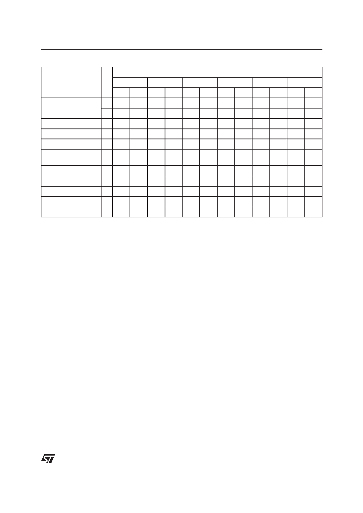
Table 5. Commands
Bus Write Operations
Command
Read/Reset
Auto Select 3 555 AA 2AA 55 555 90
Program 4 555 AA 2AA 55 555 A0 PA PD
Unlock Bypass 3 555 AA 2AA 55 555 20
Unlock Bypass
Program
Unlock Bypass Reset 2 X 90 X 00
Chip Erase 6 555 AA 2AA 55 555 80 555 AA 2AA 55 555 10
Block Erase 6+ 555 AA 2AA 55 555 80 555 AA 2AA 55 BA 30
Erase Suspend 1 X B0
Erase Resume 1 X 30
Note: X Don’t Care, PA Program Address, PD Program Data, BA Any address in the Block.
All values in the table are in hexadecimal.
The Command Interface only uses address bits A0-A10 to verify the commands, the upper address bits are Don’t Care.
Read/Reset. After a Read/Reset command, read the memory as normal until another command is issued.
Auto Select. After an Auto Select command, readManufacturer ID, Device ID or Block Protection Status.
Program, Unlock Bypass Program, Chip Erase, BlockErase. After these commands read the Status Register until the Program/Erase
Controller completes and the memory returns to Read Mode. Add additional Blocks during Block Erase Command with additional Bus Write
Operations until the Timeout Bit is set.
Unlock Bypass. After the Unlock Bypass command issue Unlock Bypass Program or Unlock Bypass Reset commands.
Unlock Bypass Reset. After the Unlock Bypass Reset command read the memory asnormal until another command is issued.
Erase Suspend. After the EraseSuspend command readnon-erasing memory blocks as normal, issue Auto Select and Program commands
on non-erasing blocks as normal.
Erase Resume. After the Erase Resume command the suspended Erase operation resumes, read the Status Register until the Program/
Erase Controller completes and the memory returns to Read Mode.
1X F0
3 555 AA 2AA 55 X F0
2X A0PAPD
1st 2nd 3rd 4th 5th 6th
Length
Addr Data Addr Data Addr Data Addr Data Addr Data Addr Data
Unlock Bypass Reset Command. The Unlock
Bypass Reset command can be used to return to
Read/Reset mode from Unlock Bypass Mode.
Two BusWrite operations are required to issuethe
Unlock Bypass Reset command.
Chip Erase Command. The Chip Erase command canbeused to erase the entire chip. SixBus
Write operations are required to issue the Chip
Erase Command and start the Program/Erase
Controller.
If any blocks are protected then these are ignored
and all the other blocks are erased. If all of the
blocks are protected the ChipErase operation appears tostart but will terminate within about100µs,
leaving the data unchanged. No error condition is
given when protected blocks are ignored.
During the erase operation the memory will ignore
all commands. It is not possible to issueany command to abort the operation. Typical chip erase
times are given in Table 6. All Bus Read operations during the Chip Erase operation will output
the Status Register on the Data Inputs/Outputs.
See the section on the Status Register for more
details.
After the Chip Erase operation has completed the
memory will return to the Read Mode, unless an
error has occurred. When an error occurs the
memory will continue to output the Status Register. A Read/Reset command must beissued to reset the error condition and return to Read Mode.
TheChip Erase Command setsall of the bits in unprotected blocks of the memory to ’1’. All previous
data is lost.
7/21
 Loading...