

查询M295V002B-120K1TR供应商
2 Mbit (256Kb x8, Boot Block) Single Supply Flash Memory
5V ± 10% SUPPLYVOLTAGEfor PROGRAM,
ERASEand READOPERATIONS
FASTACCESSTIME: 70ns
FASTPROGRAMMING TIME: 10µs typical
PROGRAM/ERASECONTROLLER(P/E.C.)
– ProgramByte-by-Byte
– Status Register bits
MEMORYBLOCKS
– Boot Block (Topor Bottomlocation)
– Parameterand Mainblocks
BLOCK, MULTI-BLOCKand CHIP ERASE
MULTI-BLOCKPROTECTION/TEMPORARY
UNPROTECTIONMODES
ERASESUSPEND and RESUMEMODES
– Read and Program anotherBlock during
Erase Suspend
LOW POWER CONSUMPTION
– Stand-byand Automatic Stand-by
100,000 PROGRAM/ERASECYCLESper
BLOCK
20 YEARSDATARETENTION
– Defectivitybelow 1ppm/year
ELECTRONICSIGNATURE
– ManufacturerCode: 20h
– Device Code, M29F002T:B0h
– Device Code, M29F002NT:B0h
– Device Code, M29F002B:34h
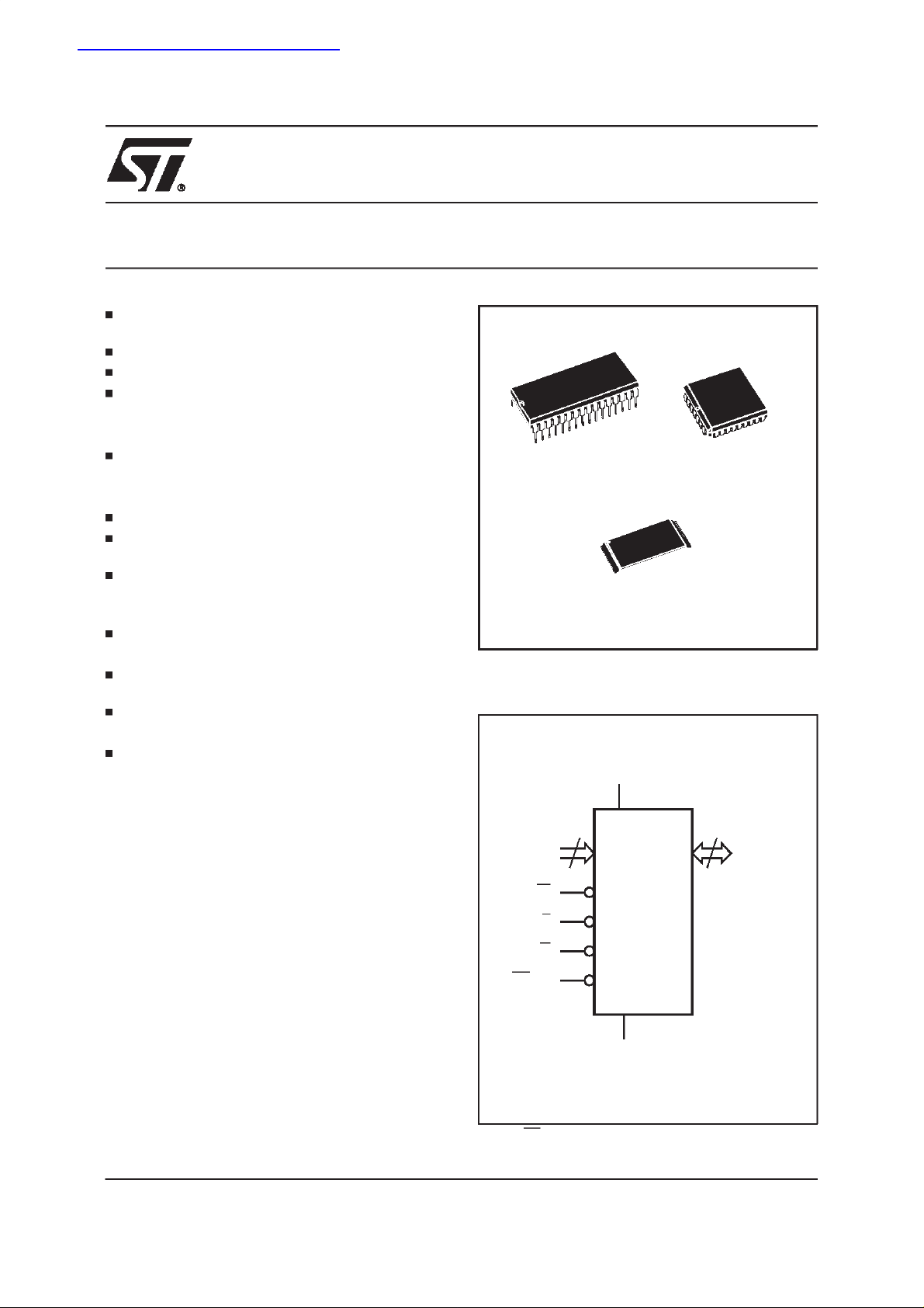
DESCRIPTION
The M29F002 is a non-volatile memory that may
beerasedelectricallyat theblock or chipleveland
programmed in-system on a Byte-by-Byte basis
usingonlyasingle5VV
Eraseoperations thenecessaryhigh voltages are
generatedinternally. The device can also be programmedin standardprogrammers.
Thearraymatrixorganisationallowseach blockto
be erased and reprogrammed without affecting
otherblocks. Blockscan be protectedagainst programing and erase on programming equipment,
and temporarily unprotected to make changes in
the application. Each block can be programmed
and erased over 100,000 cycles.
supply.ForProgramand
CC
M29F002T, M29F002NT
M29F002B
32
1
PDIP32 (P)
TSOP32 (N)
8 x 20mm
Figure1. LogicDiagram
V
CC
18
A0-A17
W
E
G
(*) RPNC
Note: * RPNC function is not available for theM29F002NT
M29F002T
M29F002B
M29F002NT
V
SS
PLCC32 (K)
8
DQ0-DQ7
AI02078C
July 1998 1/29
M29F002T, M29F002NT, M29F002B
Figure2A. DIPPin Connections
(*) RPNC V
Note: Pin 1 is notconnected forthe M29F002NT
A15
A12
A7
A6
A5
A4
A3
A2
A1
A0
DQ0
DQ2
SS
1
2
3
4
5
6
7
M29F002T
8
M29F002B
9
M29F002NT
10
11
12
13
14
15
16
32
31
30
29
28
27
26
25
24
23
22
21
20
19
18
17
AI02080C
WA16
A17
A14
A13
A8
A9
A11
G
A10
E
DQ7
DQ6
DQ5DQ1
DQ4
DQ3V
CC
Figure2B. LCC Pin Connections
CC
RPNC
V
32
DQ3
DQ4
W
DQ5
A7
A6
A5
A4
A3
A2
A1
A0
DQ0
9
A12
A15
M29F002T
M29F002B
DQ1
DQ2
A16
1
17
SS
V
A17
25
DQ6
A14
A13
A8
A9
A11
G
A10
E
DQ7
AI02079C
Figure2C. TSOPPin Connections
A11 G
A9
A8
A13
A14
A17
V
CC
RPNC
A16
A15
A12
A7
A6
A5
A4 A3
1
W
8
M29F002T
M29F002B
9
16 17
32
25
24
AI02361B
A10
E
DQ7
DQ6
DQ5
DQ4
DQ3
V
SS
DQ2
DQ1
DQ0
A0
A1
A2
Table 1. Signal Names
A0-A17 Address Inputs
DQ0-DQ7 Data Input/Outputs, Command Inputs
E Chip Enable
G Output Enable
W Write Enable
RPNC
V
CC
V
SS
(*)
Reset / Block TemporaryUnprotect
Supply Voltage
Ground
DESCRIPTION(cont’d)
Instructionsfor Read/Reset, Auto Select for read-
ing the Electronic Signature or Block Protection
status,Programming,Blockand Chip Erase,Erase
Suspend and Resume are written to thedevice in
cyclesofcommandstoa CommandInterfaceusing
standardmicroprocessorwritetimings.The device
isoffered in PLCC32,PDIP32andTSOP32(8 x20
mm)packages.
2/29
M29F002T, M29F002NT, M29F002B
Table2. Absolute Maximum Ratings
Symbol Parameter Value Unit
T
A
T
BIAS
T
STG
(2)
V
IO
V
CC
V
(A9, E, G, RPNC)
Notes: 1. Except for therating ”Operating Temperature Range”, stressesabove those listedin theTable ”AbsoluteMaximum Ratings”
may cause permanent damage to thedevice. These are stress ratings only and operation of the device at these or any other
conditions above those indicated in the Operatingsections of this specification is not implied.Exposure to Absolute Maximum
Rating conditions for extended periods may affectdevice reliability.Refer also tothe STMicroelectronics SURE Programand other
relevant quality documents.
2. Minimum Voltagemay undershoot to–2V during transitionand for less than 20ns.
3. Depends on range.
Ambient Operating Temperature
Temperature Under Bias –50 to 125 °C
Storage Temperature –65 to 150 °C
Input or Output Voltages –0.6to 7 V
Supply Voltage –0.6to 7 V
(2)
A9, E, G, RPNC Voltage –0.6to 13.5 V
Organisation
The M29F002 is organised as 256K x 8. Memory
control is provided by Chip Enable E, OutputEnable G and WriteEnableW inputs.
A Reset/Block Temporary Unprotection RPNC
(NOTavailable on M29F002NT)tri-levelinput providesa hardwareresetwhenpulledLow,andwhen
held High (at V
) temporarily unprotectsblocks
ID
previously protected allowing them to be programed and erased. Erase and Program operations
are controlled by an internal Program/Erase Controller(P/E.C.).StatusRegisterdataoutputon DQ7
providesa Data Pollingsignal, and DQ6 and DQ2
provide Togglesignals to indicate the state of the
P/E.Coperations.
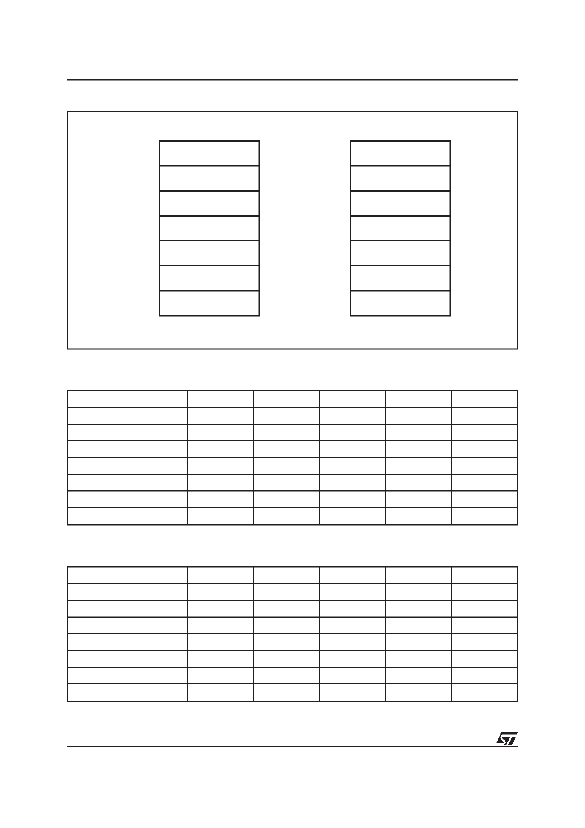
MemoryBlocks
Thedevices feature asymmetricallyblocked architecture providing system memory integration.The
M29F002hasan arrayof 7 blocks, one BootBlock
of 16 KBytes,two Parameter Blocks of 8 KBytes,
oneMainBlockof 32KBytesandthreeMainBlocks
of 64 KBytes.
Thememory map isshownin Figure3. Eachblock
can be erased separately, any combination of
blockscan be specifiedfor multi-blockerase or the
entire chip may be erased. The Erase operations
aremanagedautomaticallybytheP/E.C.Theblock
eraseoperationcan besuspendedin orderto read
(1)
(3)
–40 to 125 °C
from or program to any block not being ersased,
andthenresumed.Block protection providesadditional data security. Each block can be separately
protectedorunprotectedagainstProgramorErase
on programming equipment. All previously protectedblockscanbetemporarilyunprotectedin the
application.
Bus Operations
The following operations can be performed using
theappropriatebus cycles:Read(Array,Electronic
Signature, Block Protection Status), Write command, Output Disable,Standby,Reset, Block Protection, Unprotection, Protection Verify,
Unprotection Verify and Block Temporary Unprotection.See Tables4 and 5.
Command Interface
Instructions,made up of commands written in cycles,can be givento the Program/EraseController
through a Command Interface (C.I.). For added
dataprotection,program or erase execution starts
after4 or6 cycles.The first,second,fourthandfifth
cycles are used to input Coded cycles to the C.I.
This Coded sequence is the same for all Program/Erase Controller instructions. The ’Command’itself and its confirmation,when applicable,
are given on the third, fourth or sixth cycles. Any
incorrectcommand or any impropercommandsequencewill resetthe deviceto Read Array mode.
3/29
M29F002T, M29F002NT, M29F002B
Figure3. MemoryMap and Block AddressTable
3FFFFh
3C000h
3BFFFh
3A000h
39FFFh
38000h
37FFFh
30000h
2FFFFh
20000h
1FFFFh
10000h
0FFFFh
00000h
M29F002T, M29F002NT
16K BOOT BLOCK
8K PARAMETER BLOCK
8K PARAMETER BLOCK
32K MAIN BLOCK
64K MAIN BLOCK
64K MAIN BLOCK
64K MAIN BLOCK
3FFFFh
30000h
2FFFFh
20000h
1FFFFh
10000h
0FFFFh
08000h
07FFFh
06000h
05FFFh
04000h
03FFFh
00000h
M29F002B
64K MAIN BLOCK
64K MAIN BLOCK
64K MAIN BLOCK
32K MAIN BLOCK
8K PARAMETER BLOCK
8K PARAMETER BLOCK
16K BOOT BLOCK
Table 3A. M29F002T,M29F002NTBlock Address Table
Address Range A17 A16 A15 A14 A13
00000h-0FFFFh 0 0 X X X
10000h-1FFFFh 0 1 X X X
20000h-2FFFFh 1 0 X X X
AI02081C
30000h-37FFFh 1 1 0 X X
38000h-39FFFh 11100
3A000h-3BFFFh 11101
3C000h-3FFFFh 1111X
Table 3B. M29F002B Block Address Table
Address Range A17 A16 A15 A14 A13
00000h-03FFFh 0000X
04000h-05FFFh 00010
06000h-07FFFh 00011
08000h-0FFFFh 0 0 1 X X
10000h-1FFFFh 0 1 X X X
20000h-2FFFFh 1 0 X X X
30000h-3FFFFh 1 1 X X X
4/29

M29F002T, M29F002NT, M29F002B
Instructions
Seven instructions are defined to perform Read
Array,AutoSelect(to readthe ElectronicSignature
or BlockProtectionStatus),Program,Block Erase,
Chip Erase, Erase Suspend and Erase Resume.
The internal P/E.C. automatically handles all timing and verification of the Program and Erase
operations.The Status Register Data Polling, Toggle, Error bits may be read at any time, during
programming or erase, to monitor the progressof
the operation.
Instructionsare composedof up to sixcycles.The
first two cycles input a Coded sequence to the
CommandInterfacewhich iscommontoall instructions (see Table 8). The third cycle inputs the
instruction set-up command. Subsequent cycles
outputthe addressed data,ElectronicSignatureor
Block Protection Status for Read operations. In
orderto giveadditionaldataprotection,the instructionsfor Programand Blockor Chip Erase require
furthercommandinputs.ForaPrograminstruction,
the fourth command cycle inputs theaddressand
data to be programmed.For an Erase instruction
(Block or Chip), the fourth and fifth cycles input a
furtherCoded sequence before the Eraseconfirm
commandon thesixth cycle. Erasure of a memory
blockmaybesuspended,inordertoreaddatafrom
anotherblock or to programdata in anotherblock,
and then resumed.
When power is first applied or if V
V
, the command interface is reset to Read
LKO
falls below
CC
Array.
SIGNALDESCRIPTIONS
See Figure 1 and Table1.
AddressInputs (A0-A17).The addressinputs for
thememoryarrayarelatchedduringa write operation on the falling edge of Chip Enable E or Write
EnableW. When A9 is raised to V
, eithera Read
ID
ElectronicSignatureManufacturerorDeviceCode,
BlockProtectionStatus or a WriteBlock Protection
or BlockUnprotectionisenableddependingonthe
combinationof levels on A0,A1, A6,A12and A15.
DataInput/Outputs(DQ0-DQ7). Theinput is data
to be programmed in the memory array or a command to be written to the C.I. Both are latched on
the rising edge of Chip Enable E or Write Enable
W. Theoutput is data from the Memory Array, the
Electronic Signature Manufacturer or Device
codes, the Block Protection Status or the Status
registerData Polling bit DQ7, the ToggleBits DQ6
and DQ2, the Errorbit DQ5 or the EraseTimerbit
DQ3. Outputs are valid when Chip Enable E and
Output Enable G are active. The output is high
impedance when the chip is deselected or the
outputs are disabled and when RPNC is at a Low
level.
Chip Enable (E). The Chip Enable input activates
the memory control logic, input buffers, decoders
andsenseamplifiers.E Highdeselectsthememory
andreducesthepower consumptiontothestandby
level. E can also be used to control writing to the
commandregister and to the memory array,while
Wremainsat a low level.TheChip Enablemustbe
forcedto V
duringthe Block Unprotectionopera-
ID
tion.
OutputEnable (G). TheOutput Enable gates the
outputs through the data buffers during a read
operation. When G is High the outputs are High
impedance. G must be forced to V
level during
ID
BlockProtectionand Unprotection operations.
WriteEnable(W). This inputcontrols writingto the
CommandRegisterand Addressand Datalatches.
Reset/BlockTemporaryUnprotect/No Connect
Input (RPNC). The RPNC (not available for the
M29F002NT) input provides hardware reset and
protected block(s) temporary unprotection functions. In read or write mode, the RPNC pin can be
left open (Not Connected) or heldat V
thememory isacheived by pulling RPNC to V
. Reset of
IH
for
IL
atleast 500ns.When thereset pulseis given,if the
memory is in Read or Standby modes, it will be
availablefornewoperationsin 50nsafter the rising
edge of RPNC. If the memory is in Erase, Erase
Suspend or Program modes the reset will take
10µs.Ahardwareresetduringan EraseorProgram
operationwill corrupt the data being programmed
or the sector(s) being erased.
Temporary block unprotectionis made by holding
RPNCat V
. Inthisconditionpreviouslyprotected
ID
blockscan be programmed or erased. The transition of RPNC from V
500ns.When RPNCis returnedfrom V
to VIDmust slower than
IH
to VIHall
ID
blocks temporarily unprotected will be again protected.
Supply Voltage. The power supply for all
V
CC
operations(Read, Programand Erase).
Ground. VSSis the reference for all voltage
V
SS
measurements.
DEVICEOPERATIONS
SeeTables4, 5 and 6.
Read. Read operations are used to output the
contents of the Memory Array, the ElectronicSignature,the StatusRegisteror the BlockProtection
Status.Both Chip Enable E and Output Enable G
must be low in order to read the output of the
memory.
5/29
M29F002T, M29F002NT, M29F002B
Table4. User Bus Operations
(1)
Operation E G W RPNC
Read Byte V
Write Byte V
Output Disable V
Standby V
(6)
Reset
Block
Protection
Blocks
Unprotection
(2,4)
(4)
V
V
V
IL
V
IL
IH
V
IL
IH
XXV
IH
V
IL
IH
V
IL
V
IH
XX X VILXXXXXX Hi-Z
VIDVILPulse VIH/NC
IL
VIDVILPulse VIH/NC
ID
Block
Protection
(2,4)
Verify
V
V
IL
V
IL
IH
Block
Unprotection
(2,4)
Verify
V
IL
V
IL
IH
V
Block
Temporary
Unprotection
Notes: 1. X = VILor V
2. Block Address must be given on A13-A17 bits.
3. See Table6.
4. Operation performed onprogramming equipment.
5. RPNC can be heldat V
6. Not Availableon M29F002NT.
XX X VIDXXXXXX X
(6)
IH
or left open (Not Connected).
IH
VIH/NC
VIH/NC
VIH/NC
/NC
IH
VIH/NC
VIH/NC
(6)
A0 A1 A6 A9 A12 A15 DQ0-DQ7
(5)
A0 A1 A6 A9 A12 A15 Data Output
(5)
A0 A1 A6 A9 A12 A15 Data Input
(5)
XXXXXX Hi-Z
(5)
XXXXXX Hi-Z
(5)
XXXVIDXX X
(5)
XXXVIDV
(5)
V
V
IL
(5)
V
IL
V
IH
IL
V
V
IH
IH
V
ID
V
ID
V
IH
IH
A12 A15
A12 A15
Block Protect
Block Protect
X
Status
Status
(3)
(3)
Table5. Read ElectronicSignature (followingAS instructionor with A9 = VID)
Code Device E G W A0 A1
Manufact. Code V
M29F002T
Device Code
M29F002NT
M29F002B V
IL
V
IL
IL
V
IL
V
IL
VIL V
V
IH
V
IH
IH
V
V
V
IL
IH
IH
V
IL
V
IL
V
IL
Addresses
Don’t Care 20h
Don’t Care B0h
Don’t Care 34h
Table6. Read Block Protectionwith AS Instruction
Code E G W A0 A1 A13 - A17
Protected Block V
Unprotected Block V
IL
IL
V
IL
V
IL
V
IH
V
IH
V
IL
V
IL
V
IH
V
IH
Block Address Don’t Care 01h
Block Address Don’t Care 00h
Addresses
Other
Other
DQ0 - DQ7
DQ0 - DQ7
6/29
M29F002T, M29F002NT, M29F002B
Write.Writeoperationsareused to giveInstruction
Commandsto the memoryor to latch input data to
beprogrammed.Awrite operationisinitiatedwhen
Chip Enable E is Low and Write Enable W is Low
with OutputEnableG High.Addressesare latched
onthe fallingedgeof W or E whicheveroccurslast.
Commandsand InputDataarelatchedontherising
edge of W or E whichever occurs first.
OutputDisable.The dataoutputsare highimpedancewhen the Output EnableG is High with Write
EnableW High.
Standby. The memory is in standby when Chip
EnableE is Highand the P/E.C.is idle. The power
consumption is reduced to the standby level and
the outputs are high impedance, independent of
the Output Enable G or WriteEnable W inputs.
Automatic Standby. After 150ns of bus inactivity
and whenCMOS levels are driving the addresses,
the chip automatically enters a pseudo-standby
modewhere consumptionis reducedto the CMOS
standbyvalue, while outputsstill drive the bus.
Electronic Signature. Two codes identifying the
manufacturerand the devicecan be read fromthe
memory. These codes allow programming equipment or applications to automatically match their
interface to the characteristics of the M29F002.
The Electronic Signature is output by a Read operationwhenthe voltageappliedto A9isat V
and
ID
addressinput A1is Low.Themanufacturercodeis
output when the Address input A0 is Lowand the
devicecodewhen thisinput isHigh.OtherAddress
inputs are ignored.
TheElectronic Signaturecanalso be read, without
raisingA9to V
, bygivingthe memorythe Instruc-
ID
tionAS.
Block Protection. Each block can be separately
protected against Program or Erase on programming equipment. Block protection provides additional data security, as it disables all program or
erase operations. This mode is activated when
bothA9 and G are raisedto V
and an addressin
ID
theblock is applied on A13-A17.TheBlockProtection algorithm is shownin Figure 14. Block protectionis initiatedon theedge of Wfallingto V
after a delay of 100µs, the edge of W rising to V
. Then
IL
IH
ends the protection operations. Block protection
verify is achieved by bringing G, E, A0 and A6 to
and A1 to VIH, while W is at VIHand A9 at VID.
V
IL
Undertheseconditions,readingthedataoutputwill
yield 01h if the block defined by the inputs on
A13-A17 is protected. Any attempt to program or
erase a protected block will be ignored by the
device.
Block Temporary Unprotection. This feature is
available on M29F002T and M29F002B only. Any
previouslyprotected block can be temporarily unprotected in order to change stored data. The
temporaryunprotectionmodeisactivatedby bringing RPNC to V
. Duringthe temporary unprotec-
ID
tion mode the previously protected blocks are
unprotected.Ablock can be selectedand data can
be modified by executing the Erase or Program
instructionwiththe RPNCsignal held atV
RPNC is returned to V
, all the previously pro-
IH
. When
ID
tectedblocksare again protected.
Block Unprotection. All protected blocks can be
unprotected on programming equipment to allow
updating of bit contents. All blocks must first be
protectedbefore theunprotectionoperation.Block
unprotectionis activatedwhen A9, G and E are at
V
and A12, A15 at VIH. The Block Unprotection
ID
algorithm is shown in Figure 15. Unprotection is
initiatedbythe edgeof W fallingto V
.Afteradelay
IL
of 10ms, the unprotection operation is ended by
rising W to V
bringing G and E to V
A1 are at V
. Unprotectionverify is achieved by
IH
and A9 remains at VID. In these
IH
while A0 is at VIL, A6 and
IL
conditions,reading the output data will yield 00hif
the block defined by the inputsA13-A17has been
succesfullyunprotected.Eachblockmustbe separately verified by giving its address in order to
ensurethat it has been unprotected.
INSTRUCTIONSAND COMMANDS
The Command Interface latches commands written to the memory. Instructionsare made up from
one or more commandsto performRead Memory
Array,ReadElectronicSignature,Read Block Protection,Program, Block Erase, Chip Erase, Erase
Suspend and Erase Resume. Commands are
madeof addressand datasequences.
Table7. Commands
Hex Code Command
00h Invalid/Reserved
10h Chip Erase Confirm
20h Reserved
30h Block Erase Resume/Confirm
80h Set-up Erase
90h
A0h Program
B0h Erase Suspend
F0h Read Array/Reset
Read Electronic Signature/
Block Protection Status
7/29
M29F002T, M29F002NT, M29F002B
Table8. Instructions
(1)
Mne. Instr. Cyc. 1st Cyc. 2nd Cyc. 3rd Cyc. 4th Cyc. 5th Cyc. 6th Cyc. 7th Cyc.
RD
AS
Memory Array
(4)
AutoSelect 3+
Read/Reset
(2,4)
PG Program 4
BE BlockErase 6
(3,7)
Addr.
1+
Data F0h
(3,7)
Addr.
3+
Data AAh 55h F0h
(3,7)
Addr.
Data AAh 55h 90h
(3,7)
Addr.
Data AAh 55h A0h
(3,7)
Addr.
X
Read Memory Array until a new write cycle isinitiated.
555h AAAh 555h
Read Memory Array until a new write
cycle is initiated.
555h AAAh 555h Read Electronic Signature or Block
Protection Status until a new write cycle
is initiated. See Note 5 and 6.
555h AAAh 555h
Program
Address
Program
Read Data Polling or Toggle
Bit until Program completes.
Data
555h AAAh 555h 555h AAAh
Block
Address
Additional
Block
Data AAh 55h 80h AAh 55h 30h 30h
(3,7)
CE ChipErase 6
Addr.
555h AAAh 555h 555h AAAh 555h
Note 9
Data AAh 55h 80h AAh 55h 10h
(3,7)
ES
Notes: 1. Commands not interpreted in this table will default to read array mode.
Suspend
Erase
ER
Resume
2. Await of t
before starting any new operation (see Table14 and Figure 9).
3. X = Don’t Care.
4. The first cycles of the RD or AS instructions are followed by read operations.Any number of readcycles can occur after
the command cycles.
5. Signature Address bits A0,A1 at V
Device code.
6. Block Protection Address: A0 at V
7. For Coded cycles address inputs A12-A17are don’t care.
8. Optional, additional Blocks addresses must be entered within the erasetimeout delay after last writeentry,
timeout status can be verified through DQ3 value (see EraseTimerBit DQ3 description).
When full command is entered, read Data Polling or Togglebit until Erase is completed or suspended.
9. Read Data Polling, Togglebits or RB until Erase completes.
10.During Erase Suspend, Read and Data Programfunctions are allowed in blocks not being erased.
is necessary after a Read/Reset commandif the memory was in an Erase or Program mode
PLYH
Erase
(10)
Addr.
1
Data B0h
Addr.
1
Data 30h
IL
,A1atVIHand A13-A17 within the Block will output the Block Protection status.
IL
(3,7)
will output Manufacturer code (20h). Address bits A0 at VIHandA1 at VILwill output
X
Read until Togglestops, then read all the data needed from
any Block(s) not being erased then Resume Erase.
X
Read Data Polling or ToggleBits until Erase completesor
Erase is suspended another time
(8)
Theinstructionsrequirefrom 1 to6 cycles,the first
or first three of which are alwayswrite operations
usedtoinitiatetheinstruction.Theyarefollowedby
either further write cycles to confirmthe first commandor executethe commandimmediately.Command sequencing must be followed exactly. Any
invalid combination of commands will reset the
device to Read Array. The increased number of
cycleshas been chosen to assure maximum data
security. Instructions are initialised by two initial
Coded cycles which unlock the Command Interface.Inaddition,for Erase,instructionconfirmation
is again precededby the two Coded cycles.
8/29
StatusRegisterBits
P/E.C.statusis indicatedduring executionby Data
Polling on DQ7, detection of Toggle on DQ6 and
DQ2, or Erroron DQ5 and Erase Timer DQ3 bits.
Any read attempt during Program or Erase commandexecutionwill automaticallyoutputthesefive
StatusRegisterbits. TheP/E.C. automaticallysets
bits DQ2, DQ3, DQ5, DQ6 and DQ7. Other bits
(DQ0, DQ1 and DQ4) are reservedfor future use
and should be masked. See Tables9 and 10.
M29F002T, M29F002NT, M29F002B
Table 9. Status Register Bits
DQ Name Logic Level Definition Note
’1’
Data
7
Polling
’0’ Erase On-going
DQ
DQ Program On-going
Erase Complete or erase
block in Erase Suspend
Program Complete or data
of non erase block during
Erase Suspend
Indicates the P/E.C. status, check during
Program or Erase, and on completion
before checking bits DQ5 for Program or
Erase Success.
6 ToggleBit
5 Error Bit
4 Reserved
Erase
3
Time Bit
2 ToggleBit
’-1-0-1-0-1-0-1-’ Erase or Program On-going Successive reads outputcomplementary
DQ Program Complete
’-1-1-1-1-1-1-1-’
’1’ Program or Erase Error
’0’ Program or Erase On-going
’1’ Erase TimeoutPeriod Expired
’0’
’-1-0-1-0-1-0-1-’
1
DQ
Erase Complete or Erase
Suspend on currently
addressed block
Erase TimeoutPeriod
On-going
Chip Erase, Erase or Erase
Suspend on the currently
addressed block.
Erase Error due to the
currently addressed block
(when DQ5 = ’1’).
Program on-going, Erase
on-going on another block or
Erase Complete
Erase Suspend read on
non Erase Suspend block
data on DQ6 while Programming or Erase
operations are on-going. DQ6 remains at
constant level when P/E.C. operations are
completed or Erase Suspend is
acknowledged.
This bitis setto ’1’in the case of
Programming or Erase failure.
P/E.C. Erase operation has started. Only
possible command entry is Erase Suspend
(ES).
An additionalblock to be erased in parallel
can be entered to the P/E.C.
Indicates the erase status and allows to
identify the erased block
1 Reserved
0 Reserved
Notes: Logic level ’1’is High, ’0’ is Low.-0-1-0-0-0-1-1-1-0- represent bit value in successive Read operations.
Data Polling Bit (DQ7). WhenProgramming op-
erations are in progress, this bit outputs the complement of the bit being programmed on DQ7.
DuringEraseoperation,it outputsa ’0’.After completionof the operation, DQ7 will output the bit last
programmed or a ’1’after erasing. Data Polling is
valid and only effective during P/E.C. operation,
that is after the fourth W pulse for programmingor
after the sixth W pulse for erase. It must be performedat theaddress being programmed or at an
address within the block being erased. If all the
blocksselectedforerasureare protected,DQ7will
beset to ’0’for about 100µs,and thenreturnto the
previousaddressedmemory data value.
9/29
 Loading...