

查询M29DW324DB供应商
32 Mbit (4Mb x8 or 2Mb x16, Dual Bank 16:16, Boot Block)
FEATURES SUMMARY
■ SUPPLY VOLTAGE
–V
–V
■ ACCESS TIME: 70, 90ns
■ PROGRAMMING TIME
– 10µs per Byte/Word typical
– Double Word/ Quadruple Byte Program
■ MEMORY BLOCKS
– Dual Bank Memory Array: 16Mbit+16Mbit
– Parameter Blocks (Top or Bott o m Locati o n)
■ DUAL OPERATIONS
– Read in one bank while Program or Erase in
■ ERASE SUSPEND and RESUME MODES
– Read and Program another Block during
■ UNLOCK BYPASS PROGRAM COMMAND
– Faster Production/Batch Programm ing
■ V
PP
PROTECT
■ TEMPORARY BLOCK UNPROTECTION
MODE
■ COMMON FLASH INTERFACE
– 64 bit Security Code
■ EXTENDED MEMORY BL OCK
– Extra block used as security block or to store
■ LOW POWER CONSUMPTION
– Standby and Automatic Standby
■ 100,000 PROGRAM/ER ASE CYCL ES per
BLOCK
■ ELECTRONIC SIGNATURE
– Manufacturer Code: 0020h
– Top Device Code M29DW324DT: 225Ch
– Bottom Device Code M29DW324DB: 225Dh
2.7V to 3.6V for Program, Erase and
CC =
Read
=12V for Fast Program (optional)
PP
other
Erase Suspend
/WP PIN for FAST PROGRAM and W R IT E
additional information
M29DW324DT
M29DW324DB
3V Supply Fl ash Mem ory
Figure 1. Packages
TSOP48 (N)
12 x 20mm
FBGA
TFBGA63 (ZA)
7 x 11mm
FBGA
TFBGA48 (ZE)
6 x 8mm
1/49June 2003

M29DW324DT, M29DW324DB
TABLE OF CONTENTS
SUMMARY DESCRIPTION. . . . . . . . . . . . . . . . . . . . . . . . . . . . . . . . . . . . . . . . . . . . . . . . . . . . . . . . . . . 5
Figure 2. Logic Diagram . . . . . . . . . . . . . . . . . . . . . . . . . . . . . . . . . . . . . . . . . . . . . . . . . . . . . . . . . . 5
Table 1. Signal Names . . . . . . . . . . . . . . . . . . . . . . . . . . . . . . . . . . . . . . . . . . . . . . . . . . . . . . . . . . . 5
Figure 3. TSOP Connections . . . . . . . . . . . . . . . . . . . . . . . . . . . . . . . . . . . . . . . . . . . . . . . . . . . . . . . 6
Figure 4. TFBGA63 Connections (Top view through package). . . . . . . . . . . . . . . . . . . . . . . . . . . . . 7
Figure 5. TFBGA48 Connections (Top view through package). . . . . . . . . . . . . . . . . . . . . . . . . . . . . 8
Table 2. Bank Architecture . . . . . . . . . . . . . . . . . . . . . . . . . . . . . . . . . . . . . . . . . . . . . . . . . . . . . . . . 8
Figure 6. Block Addresses (x8). . . . . . . . . . . . . . . . . . . . . . . . . . . . . . . . . . . . . . . . . . . . . . . . . . . . . 9
Figure 7. Block Addresses (x16). . . . . . . . . . . . . . . . . . . . . . . . . . . . . . . . . . . . . . . . . . . . . . . . . . . 10
SIGNAL DESCRIPTIONS . . . . . . . . . . . . . . . . . . . . . . . . . . . . . . . . . . . . . . . . . . . . . . . . . . . . . . . . . . . 11
Address Inputs (A0-A20). . . . . . . . . . . . . . . . . . . . . . . . . . . . . . . . . . . . . . . . . . . . . . . . . . . . . . . . . 11
Data Inputs/Outputs (DQ0-DQ7). . . . . . . . . . . . . . . . . . . . . . . . . . . . . . . . . . . . . . . . . . . . . . . . . . . 11
Data Inputs/Outputs (DQ8-DQ14 ). . . . . . . . . . . . . . . . . . . . . . . . . . . . . . . . . . . . . . . . . . . . . . . . . .11
Data Input/Output or Address Input (DQ15A–1). . . . . . . . . . . . . . . . . . . . . . . . . . . . . . . . . . . . . . . . 11
Chip Enable (E). . . . . . . . . . . . . . . . . . . . . . . . . . . . . . . . . . . . . . . . . . . . . . . . . . . . . . . . . . . . . . . . 11
Output Enable (G). . . . . . . . . . . . . . . . . . . . . . . . . . . . . . . . . . . . . . . . . . . . . . . . . . . . . . . . . . . . . . 11
Write Enable (W). . . . . . . . . . . . . . . . . . . . . . . . . . . . . . . . . . . . . . . . . . . . . . . . . . . . . . . . . . . . . . . 11
V
Write Protect (V
PP/
Reset/Block Temporary Unprotect (RP).. . . . . . . . . . . . . . . . . . . . . . . . . . . . . . . . . . . . . . . . . . . . .11
Ready/Busy Output (RB). . . . . . . . . . . . . . . . . . . . . . . . . . . . . . . . . . . . . . . . . . . . . . . . . . . . . . . . . 1 1
Byte/Word Organization Select (BYTE). . . . . . . . . . . . . . . . . . . . . . . . . . . . . . . . . . . . . . . . . . . . . . 12
V
Supply Voltage (2.7V to 3.6V).. . . . . . . . . . . . . . . . . . . . . . . . . . . . . . . . . . . . . . . . . . . . . . . . .12
CC
Ground. . . . . . . . . . . . . . . . . . . . . . . . . . . . . . . . . . . . . . . . . . . . . . . . . . . . . . . . . . . . . . . . . . . 12
V
SS
WP). . . . . . . . . . . . . . . . . . . . . . . . . . . . . . . . . . . . . . . . . . . . . . . . . . . . . . . 11
PP/
BUS OPERATIONS. . . . . . . . . . . . . . . . . . . . . . . . . . . . . . . . . . . . . . . . . . . . . . . . . . . . . . . . . . . . . . . . 13
Bus Read. . . . . . . . . . . . . . . . . . . . . . . . . . . . . . . . . . . . . . . . . . . . . . . . . . . . . . . . . . . . . . . . . . . . . 13
Bus Write. . . . . . . . . . . . . . . . . . . . . . . . . . . . . . . . . . . . . . . . . . . . . . . . . . . . . . . . . . . . . . . . . . . . . 13
Output Disable. . . . . . . . . . . . . . . . . . . . . . . . . . . . . . . . . . . . . . . . . . . . . . . . . . . . . . . . . . . . . . . . . 13
Standby. . . . . . . . . . . . . . . . . . . . . . . . . . . . . . . . . . . . . . . . . . . . . . . . . . . . . . . . . . . . . . . . . . . . . . 13
Automatic Standby. . . . . . . . . . . . . . . . . . . . . . . . . . . . . . . . . . . . . . . . . . . . . . . . . . . . . . . . . . . . . . 13
Special Bus Operations . . . . . . . . . . . . . . . . . . . . . . . . . . . . . . . . . . . . . . . . . . . . . . . . . . . . . . . . 1 3
Electronic Signature. . . . . . . . . . . . . . . . . . . . . . . . . . . . . . . . . . . . . . . . . . . . . . . . . . . . . . . . . . . . . 13
Block Protect and Chip Unprotect. . . . . . . . . . . . . . . . . . . . . . . . . . . . . . . . . . . . . . . . . . . . . . . . . . 13
Block Protect and Chip Unprotect. . . . . . . . . . . . . . . . . . . . . . . . . . . . . . . . . . . . . . . . . . . . . . . . . . 13
Table 3. Bus Operations, BYTE = V
Table 4. Bus Operations, BYTE = V
. . . . . . . . . . . . . . . . . . . . . . . . . . . . . . . . . . . . . . . . . . . . . . . 14
IL
. . . . . . . . . . . . . . . . . . . . . . . . . . . . . . . . . . . . . . . . . . . . . . . 14
IH
COMMAND INTERFACE . . . . . . . . . . . . . . . . . . . . . . . . . . . . . . . . . . . . . . . . . . . . . . . . . . . . . . . . . . . 15
Read/Reset Command . . . . . . . . . . . . . . . . . . . . . . . . . . . . . . . . . . . . . . . . . . . . . . . . . . . . . . . . . . 15
Auto Select Command. . . . . . . . . . . . . . . . . . . . . . . . . . . . . . . . . . . . . . . . . . . . . . . . . . . . . . . . . . . 15
Program Command. . . . . . . . . . . . . . . . . . . . . . . . . . . . . . . . . . . . . . . . . . . . . . . . . . . . . . . . . . . . . 15
Fast Program Commands . . . . . . . . . . . . . . . . . . . . . . . . . . . . . . . . . . . . . . . . . . . . . . . . . . . . . . . . 16
2/49

M29DW324DT, M29DW324DB
Quadruple Byte Program Command. . . . . . . . . . . . . . . . . . . . . . . . . . . . . . . . . . . . . . . . . . . . . . . . 16
Double Word Program Command. . . . . . . . . . . . . . . . . . . . . . . . . . . . . . . . . . . . . . . . . . . . . . . . . . 16
Unlock Bypass Command. . . . . . . . . . . . . . . . . . . . . . . . . . . . . . . . . . . . . . . . . . . . . . . . . . . . . . . . 16
Unlock Bypass Program Command. . . . . . . . . . . . . . . . . . . . . . . . . . . . . . . . . . . . . . . . . . . . . . . . . 16
Unlock Bypass Reset Command. . . . . . . . . . . . . . . . . . . . . . . . . . . . . . . . . . . . . . . . . . . . . . . . . . .16
Chip Erase Command. . . . . . . . . . . . . . . . . . . . . . . . . . . . . . . . . . . . . . . . . . . . . . . . . . . . . . . . . . . 16
Block Erase Command.. . . . . . . . . . . . . . . . . . . . . . . . . . . . . . . . . . . . . . . . . . . . . . . . . . . . . . . . . . 17
Erase Suspend Comma nd. . . . . . . . . . . . . . . . . . . . . . . . . . . . . . . . . . . . . . . . . . . . . . . . . . . . . . . . 17
Erase Resume Command. . . . . . . . . . . . . . . . . . . . . . . . . . . . . . . . . . . . . . . . . . . . . . . . . . . . . . . . 17
Enter Extended Block Command . . . . . . . . . . . . . . . . . . . . . . . . . . . . . . . . . . . . . . . . . . . . . . . . . .18
Exit Extended Block Command. . . . . . . . . . . . . . . . . . . . . . . . . . . . . . . . . . . . . . . . . . . . . . . . . . . . 18
Table 5. Commands, 16-bit mode, BYTE = V
Table 6. Commands, 8-bit mode, BYTE = V
Table 7. Program, Erase Times and Program, Erase Endurance Cycles . . . . . . . . . . . . . . . . . . . . 19
STATUS REGISTER. . . . . . . . . . . . . . . . . . . . . . . . . . . . . . . . . . . . . . . . . . . . . . . . . . . . . . . . . . . . . . . 20
Data Polling Bit (DQ7). . . . . . . . . . . . . . . . . . . . . . . . . . . . . . . . . . . . . . . . . . . . . . . . . . . . . . . . . . . 20
Toggle Bit (DQ6).. . . . . . . . . . . . . . . . . . . . . . . . . . . . . . . . . . . . . . . . . . . . . . . . . . . . . . . . . . . . . . . 20
Error Bit (DQ5). . . . . . . . . . . . . . . . . . . . . . . . . . . . . . . . . . . . . . . . . . . . . . . . . . . . . . . . . . . . . . . . . 20
Erase Timer Bit (DQ3). . . . . . . . . . . . . . . . . . . . . . . . . . . . . . . . . . . . . . . . . . . . . . . . . . . . . . . . . . . 20
Alternative Toggle Bit (DQ2).. . . . . . . . . . . . . . . . . . . . . . . . . . . . . . . . . . . . . . . . . . . . . . . . . . . . . . 20
Table 8. Status Register Bits. . . . . . . . . . . . . . . . . . . . . . . . . . . . . . . . . . . . . . . . . . . . . . . . . . . . . . 21
Figure 8. Data Polling Flowchart . . . . . . . . . . . . . . . . . . . . . . . . . . . . . . . . . . . . . . . . . . . . . . . . . . . 21
Figure 9. Data Toggle Flowchart. . . . . . . . . . . . . . . . . . . . . . . . . . . . . . . . . . . . . . . . . . . . . . . . . . . 2 1
. . . . . . . . . . . . . . . . . . . . . . . . . . . . . . . . . . . . . . .18
IH
. . . . . . . . . . . . . . . . . . . . . . . . . . . . . . . . . . . . . . . . . 19
IL
MAXIMUM RATING. . . . . . . . . . . . . . . . . . . . . . . . . . . . . . . . . . . . . . . . . . . . . . . . . . . . . . . . . . . . . . . . 22
Table 9. Absolute Maximum Ratings. . . . . . . . . . . . . . . . . . . . . . . . . . . . . . . . . . . . . . . . . . . . . . . .22
DC and AC PARAMETERS . . . . . . . . . . . . . . . . . . . . . . . . . . . . . . . . . . . . . . . . . . . . . . . . . . . . . . . . . 23
Table 10. Operating and AC Measurement Conditions. . . . . . . . . . . . . . . . . . . . . . . . . . . . . . . . . . 23
Figure 10. AC Measurement I/O Waveform . . . . . . . . . . . . . . . . . . . . . . . . . . . . . . . . . . . . . . . . . .23
Figure 11. AC Measurement Load Circuit. . . . . . . . . . . . . . . . . . . . . . . . . . . . . . . . . . . . . . . . . . . . 23
Table 11. Device Capacitance . . . . . . . . . . . . . . . . . . . . . . . . . . . . . . . . . . . . . . . . . . . . . . . . . . . . . 23
Table 12. DC Characteristics. . . . . . . . . . . . . . . . . . . . . . . . . . . . . . . . . . . . . . . . . . . . . . . . . . . . . . 24
Figure 12. Read Mode AC Waveforms . . . . . . . . . . . . . . . . . . . . . . . . . . . . . . . . . . . . . . . . . . . . . . 25
Table 13. Read AC Characteristics . . . . . . . . . . . . . . . . . . . . . . . . . . . . . . . . . . . . . . . . . . . . . . . . . 25
Figure 13. Write AC Waveforms, Write Enable Controlled . . . . . . . . . . . . . . . . . . . . . . . . . . . . . . . 26
Table 14. Write AC Characteristics, Write Enable Controlled . . . . . . . . . . . . . . . . . . . . . . . . . . . . . 26
Figure 14. Write AC Waveforms, Chip Enable Controlled . . . . . . . . . . . . . . . . . . . . . . . . . . . . . . . .27
Table 15. Write AC Characteristics, Chip Enable Controlled . . . . . . . . . . . . . . . . . . . . . . . . . . . . . 27
Figure 15. Reset/Block Temporary Unprotect AC Waveforms . . . . . . . . . . . . . . . . . . . . . . . . . . . . 28
Table 16. Reset/Block Temporary Unprotect AC Characteristi cs . . . . . . . . . . . . . . . . . . . . . . . . . . 28
Figure 16. Accelerated Program Timing Waveforms. . . . . . . . . . . . . . . . . . . . . . . . . . . . . . . . . . . . 28
PACKAGE MECHANICAL . . . . . . . . . . . . . . . . . . . . . . . . . . . . . . . . . . . . . . . . . . . . . . . . . . . . . . . . . . 29
Figure 17. 48 Lead Plastic Thin Small Outline, 12x20 mm, Bottom View Package Outline . . . . . . 29
3/49

M29DW324DT, M29DW324DB
Table 17. 48 Lead Plastic Thin Small Outline, 12x20 mm, Package Mechanical Data . . . . . . . . . . 29
Figure 18. TFBGA63 7x11mm - 6x8 Ball Array, 0.8mm Pitch, Bottom View Package Outli ne . . . . 30
Table 18. TFBGA63 7x11mm - 6x8 Ball Array, 0.8mm Pitch, Package Mechanical Data. . . . . . . . 30
Figure 19. TFBGA48 6x8mm - 6x8 Ball Array, 0.8mm Pitch, Bottom View Package Outlin e . . . . . 31
Table 19. TFBGA48 6x8mm - 6x8 Ball Array, 0.8mm Pitch, Package Mechanical Data. . . . . . . . . 31
PART NUMBERING . . . . . . . . . . . . . . . . . . . . . . . . . . . . . . . . . . . . . . . . . . . . . . . . . . . . . . . . . . . . . . . 32
Table 20. Ordering Information Scheme . . . . . . . . . . . . . . . . . . . . . . . . . . . . . . . . . . . . . . . . . . . . .32
APPENDIX A. BLOCK ADDRESSES. . . . . . . . . . . . . . . . . . . . . . . . . . . . . . . . . . . . . . . . . . . . . . . . . . 33
Table 21. Top Boot Block Addresses, M29DW324DT . . . . . . . . . . . . . . . . . . . . . . . . . . . . . . . . . . 33
Table 22. Bottom Boot Block Addresses, M29DW324DB. . . . . . . . . . . . . . . . . . . . . . . . . . . . . . . . 36
APPENDIX B. COMMON FLASH INT ERFACE (CFI) . . . . . . . . . . . . . . . . . . . . . . . . . . . . . . . . . . . . . 39
Table 23. Query Structure Overview. . . . . . . . . . . . . . . . . . . . . . . . . . . . . . . . . . . . . . . . . . . . . . . .39
Table 24. CFI Query Identification String . . . . . . . . . . . . . . . . . . . . . . . . . . . . . . . . . . . . . . . . . . . .39
Table 25. CFI Query System Interface Information. . . . . . . . . . . . . . . . . . . . . . . . . . . . . . . . . . . . . 40
Table 26. Device Geometry Definition. . . . . . . . . . . . . . . . . . . . . . . . . . . . . . . . . . . . . . . . . . . . . . .40
Table 27. Primary Algorithm-Specific Extended Query Table . . . . . . . . . . . . . . . . . . . . . . . . . . . . . 41
Table 28. Security Code Area . . . . . . . . . . . . . . . . . . . . . . . . . . . . . . . . . . . . . . . . . . . . . . . . . . . . . 41
APPENDIX C. EXTENDED MEMORY BLOCK . . . . . . . . . . . . . . . . . . . . . . . . . . . . . . . . . . . . . . . . . . 42
Factory Locked Extended Block . . . . . . . . . . . . . . . . . . . . . . . . . . . . . . . . . . . . . . . . . . . . . . . . . 42
Customer Lockable Extended Block. . . . . . . . . . . . . . . . . . . . . . . . . . . . . . . . . . . . . . . . . . . . . . 42
Table 29. Extended Block Address and Data . . . . . . . . . . . . . . . . . . . . . . . . . . . . . . . . . . . . . . . . . 42
APPENDIX D. BLOCK PROTECTION . . . . . . . . . . . . . . . . . . . . . . . . . . . . . . . . . . . . . . . . . . . . . . . . . 43
Programmer Technique . . . . . . . . . . . . . . . . . . . . . . . . . . . . . . . . . . . . . . . . . . . . . . . . . . . . . . . . 43
In-System Technique . . . . . . . . . . . . . . . . . . . . . . . . . . . . . . . . . . . . . . . . . . . . . . . . . . . . . . . . . . 43
Table 30. Programmer Technique Bus Operations, BYTE = V
or VIL . . . . . . . . . . . . . . . . . . . . .43
IH
Figure 20. Programmer Equipment Group Protect Flowchart. . . . . . . . . . . . . . . . . . . . . . . . . . . . . 44
Figure 21. Programmer Equipment Chip Unprotect Flowchart . . . . . . . . . . . . . . . . . . . . . . . . . . . . 45
Figure 22. In-System Equipment G roup Protect Flowchart. . . . . . . . . . . . . . . . . . . . . . . . . . . . . . . 46
Figure 23. In-System Equipment Chip Unprotect Flowchart . . . . . . . . . . . . . . . . . . . . . . . . . . . . . . 47
REVISION HISTORY. . . . . . . . . . . . . . . . . . . . . . . . . . . . . . . . . . . . . . . . . . . . . . . . . . . . . . . . . . . . . . . 48
Table 31. Document Revision History . . . . . . . . . . . . . . . . . . . . . . . . . . . . . . . . . . . . . . . . . . . . . . .48
4/49
SUMMARY DESCRIPTION
The M29DW324D is a 32 Mbit (4Mb x8 or 2Mb
x16) non-volatile memory that can be read, erased
and reprogrammed. These operations can be performed using a single low voltage (2.7 to 3.6V)
supply. On power-up the memory d efaults to its
Read mode where it can be read in the same way
as a ROM or EPROM.
The device features an asymmet rical block architecture. The M29DW324D has an array of 8 parameter and 63 main blocks and is divided into two
Banks, A and B, providing Dual Bank operations.
While programming or erasing in Bank A, read operations are possible in Bank B and vice versa.
Only one bank at a time is allowed to be in program or erase mode. The bank architecture is
summarized in Table 2. M29DW324DT locates the
Parameter Blocks at the top of the memory address space while the M29DW324DB locates the
Parameter Blocks starting from the bottom.
M29DW324D h as an extra 32 KWord (x16 mode)
or 64 KByte (x8 mode) block, the Extended Block,
that can be accessed using a dedicated command. The Extended Block can be protected and
so is useful for storing security information. How-
M29DW324DT, M29DW324DB
ever the protection is irreversible, once protected
the protection cannot be undone.
Each block can be erased indep endently so it is
possible to preserve valid dat a while old data is
erased. The blocks can be protected to prevent
accidental Program or Erase commands from
modifying the memory. Program and E rase commands are written to the Command Interface of
the memory. An on-chip Program/Erase Controller
simplifies the process of prog ramming or eras ing
the memory by taking care of all of the special operations that are required to update the memory
contents. The end of a program or erase operation
can be detected and any error conditions identified. The command set required to control the
memory is consistent with JEDEC standards.
Chip Enable, Output Enable and Write Enable signals control the bus operation of the memory.
They allow simple conne ction to most m icroprocessors, often without additional logic.
The memory is offered in TSOP48 (12x20mm),
TFBGA63 (7x11mm, 0.8mm pitch) and TFBGA48
(6x8mm, 0.8mm pitch) packages. The memory is
supplied with all the bi t s erased (set t o ’1’).
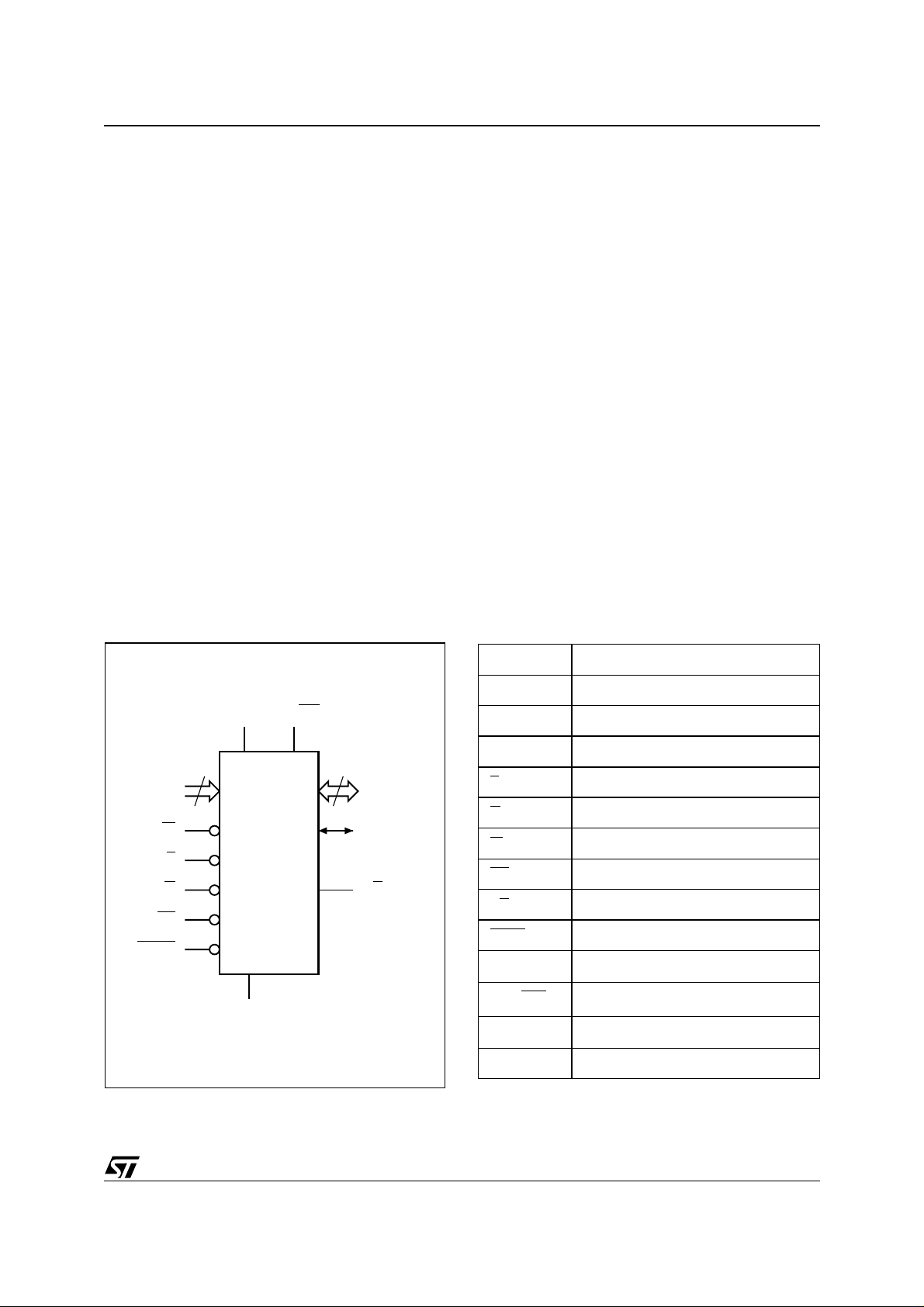
Figure 2. Logic Diagram Table 1. Signal Names
A0-A20 Address Inputs
DQ0-DQ7 Data Inputs/Outputs
VPP/WP
V
A0-A20
W
RP
BYTE
CC
21
E
G
M29DW324DT
M29DW324DB
V
SS
15
DQ0-DQ14
DQ15A–1
RB
AI06867B
DQ8-DQ14 Data Inputs/Outputs
DQ15A–1 Data Input/Output or Address Input
E
G
W
RP
RB
BYTE
V
CC
VPP/WP
V
SS
NC Not Connected Internally
Chip Enable
Output Enable
Write Enable
Reset/Block Temporary Unprotect
Ready/Busy Output
Byte/Word Organization Select
Supply Voltage
VPP/Write Protect
Ground
5/49
M29DW324DT, M29DW324DB
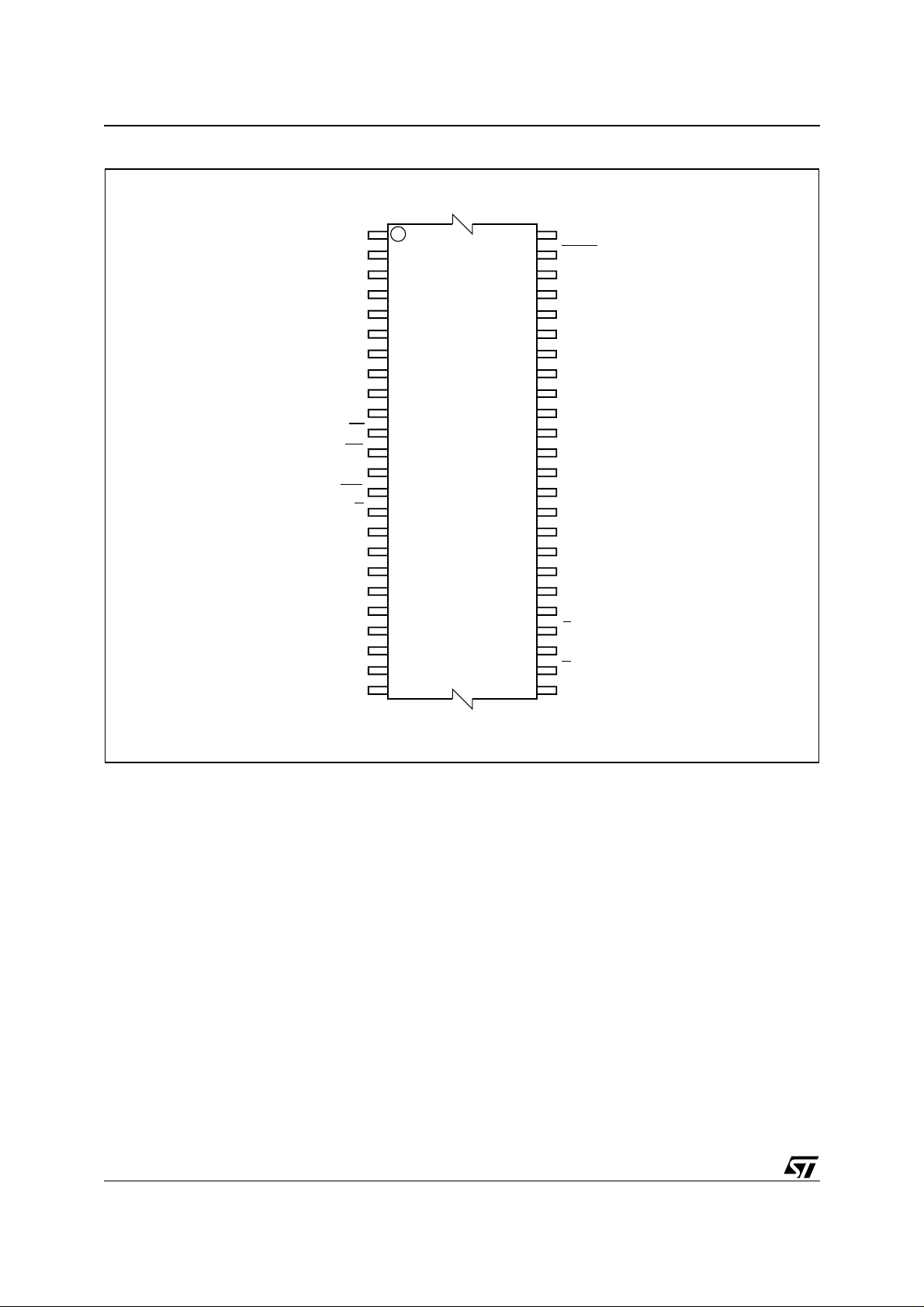
Figure 3. TSOP Connections
A15
1
48
A14
A13
A12
A11
A10 DQ14
A9
A8
A19
A20
M29DW324DT
M29DW324DB
W
RP
NC
12
13
37
36
VPP/WP
RB
A18
A17
A7
A6
A5
A4
A3
A2
A1
24 25
A16
BYTE
V
SS
DQ15A–1
DQ7
DQ6
DQ13
DQ5
DQ12
DQ4
V
CC
DQ11
DQ3
DQ10
DQ2
DQ9
DQ1
DQ8
DQ0
G
V
SS
E
A0
6/49
AI06805
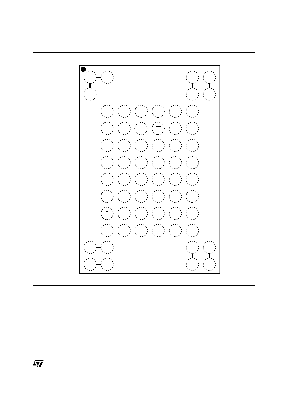
Figure 4. TFBGA63 Conn ections (Top view through packa ge)
M29DW324DT, M29DW324DB
654321
A
B
NC
NC
(1)
(1)
C
D
E
F
G
H
NC
A3
A4
A2
A1
A0
(1)
A7
A17
A6
RB
V
/
PP
A18
A5 A20
DQ0
E
DQ8
DQ2
DQ10
WP
W
RP
NC
A19
DQ5
DQ12
A9
A8
A10
A11
DQ7
DQ14
NC
NC
A13
A12
A14
A15
A16
BYTE
(1)
(1)
NC
NC
87
(1)
(1)
J
K
L
NC
M
NC
G
V
SS
(1)
NC
(1)
NC
DQ9
DQ1
(1)
(1)
DQ11
DQ3
V
CC
DQ4
Note: 1. Balls are shorted together via the substrate but not connecte d to the die.
DQ13
DQ6
DQ15
A–1
V
SS
NC
NC
NC
NC
(1)
(1)
AI05525B
(1)
(1)
7/49
M29DW324DT, M29DW324DB
Figure 5. TFBGA48 Connections (Top view through package)
654321
V
PP
A18
DQ2
DQ10
DQ11
DQ3
RB
/WP
A
B
C
D
E
F
G
H
A3
A4
A2
A1
A0
E
G
V
SS
A7
A17
A6
A5 A20
DQ0
DQ8
DQ9
DQ1
W
RP
NC
A19
DQ5
DQ12
V
CC
DQ4
A9
A8
A10
A11
DQ7
DQ14
DQ13
DQ6
A13
A12
A14
A15
A16
BYTE
DQ15
A–1
V
SS
Table 2. Bank Architecture
Bank Bank Size
A 16 Mbit 8 8KByte/ 4 KWord 31 64KByte/ 32 KWord
B 16 Mbit — — 32 64KByte/ 32 KWord
Parameter Blocks Main Blocks
No. of
Blocks
Block Size No. of Blocks Block Size
AI08084
8/49
Figure 6. Block Addresses (x8)
M29DW324DT, M29DW324DB
Bank B
Bank A
Top Boot Block (x8)
Address lines A20-A0, DQ15A-1
000000h
00FFFFh
1F0000h
1FFFFFh
200000h
20FFFFh
3E0000h
3EFFFFh
3F0000h
3F1FFFh
64 KByte or
32 KWord
64 KByte or
32 KWord
64 KByte or
32 KWord
64 KByte or
32 KWord
8 KByte or
4 KWord
Total of 32
Main Blocks
Total of 31
Main Blocks
Total of 8
Parameter
(1)
Blocks
Bank A
Bank B
Bottom Boot Block (x8)
Address lines A20-A0, DQ15A-1
000000h
001FFFh
00E000h
00FFFFh
010000h
01FFFFh
1F0000h
1FFFFFh
200000h
20FFFFh
8 KByte or
4 KWord
8 KByte or
4 KWord
64 KByte or
32 KWord
64 KByte or
32 KWord
64 KByte or
32 KWord
Total of 8
Parameter
(1)
Blocks
Total of 31
Main Blocks
Total of 32
Main Blocks
3FE000h
3FFFFFh
Note: 1. Used as Extended Block Addre ss es in Exten ded Block mode.
2. Also see Appendix A, Tabl es 21 and 22 for a full l i st i ng of the Block Addresses .
8 KByte or
4 KWord
3F0000h
3FFFFFh
64 KByte or
32 KWord
AI06803
9/49
M29DW324DT, M29DW324DB
Figure 7. Block Addresses (x16)
Bank B
Bank A
000000h
007FFFh
0F8000h
0FFFFFh
100000h
107FFFh
1F0000h
1F7FFFh
1F8000h
1F8FFFh
Top Boot Block (x16)
Address lines A20-A0
64 KByte or
32 KWord
64 KByte or
32 KWord
64 KByte or
32 KWord
64 KByte or
32 KWord
8 KByte or
4 KWord
Total of 32
Main Blocks
Total of 31
Main Blocks
Total of 8
Parameter
(1)
Blocks
Bank A
Bank B
000000h
000FFFh
007000h
007FFFh
008000h
00FFFFh
0F8000h
0FFFFFh
100000h
107FFFh
Bottom Boot Block (x16)
Address lines A20-A0
8 KByte or
4 KWord
8 KByte or
4 KWord
64 KByte or
32 KWord
64 KByte or
32 KWord
64 KByte or
32 KWord
Total of 8
Parameter
(1)
Blocks
Total of 31
Main Blocks
Total of 32
Main Blocks
1FF000h
1FFFFFh
Note: 1. Used as Extended Block Addre ss es in Exten ded Block mode.
2. Also see Appendix A, Tables 21 and 22 for a full listi ng of the Block Addresses.
8 KByte or
4 KWord
1F8000h
1FFFFFh
64 KByte or
32 KWord
AI05555
10/49

SIGNAL DESCRIPTIONS
See Figure 2, Logic Diagram, and Table 1, Sign al
Names, for a brief overview of the signals connected to this device.
Address Inputs (A0-A20). The Address Inputs
select the cells i n the memory array to a ccess during Bus Read operations. During Bus Write operations they control the commands sent to the
Command Interface of the Program/Erase Controller.
Data Inputs/Outputs (DQ0-DQ7). The Data I/O
outputs the data stored at the selected address
during a Bus Read operation. During Bus Write
operations they represent the commands sent to
the Command Interface of the Program/Erase
Controller.
Data Inputs/Outputs (DQ8-DQ14). The Data I/O
outputs the data stored at the selected address
during a Bus Read operation when B Y TE
V
. When BYTE is Low, VIL, these pins are not
IH
is High,
used and are high impedance. During Bus Write
operations the Command Register does not use
these bits. When reading the Status Register
these bits should be ignored.
Data Input/Output o r Address Input (DQ15A –1).
When BYTE
is High, VIH, this pin behaves as a
Data Input/Output pin (as DQ8-DQ14). When
is Low, VIL, this pin behaves as an address
BYTE
pin; DQ15A–1 Low will select the LSB of the addressed Word, DQ15A–1 High will select the MSB.
Throughout the text consider references to the
Data Input/Output to include this pin when BYTE
is
High and references to the Address Inputs to include this pin when BYTE
is Low except when
stated explicitly otherwise.
Chip Enable (E
). The Chip Enable, E, activates
the memory, allowing Bus Read and Bus Write operations to be performed. When Chip Enable is
High, V
Output Enable (G
, all other pins are ignored.
IH
). The Output Enable, G, con-
trols the Bus Read operation of the memory.
Write Enable (W
). The Write Enable, W, controls
the Bus Write operation of the memory’s Command Interf a c e .
Write Protect (VPP/WP). The VPP/Write
V
PP/
Protect
pin provides two functions. The VPP function allo ws the memory to use an exte rnal high
volt age power suppl y t o reduce the time required
for P rogram operatio ns. This i s achi eved by bypassing the unlock cycles an d/or using the Double Word or Quadruple Byte Program commands.
The Write Protect function provides a hardware
method of protecting the two outermost boot
blocks.
When VPP/Write Protect is L ow , VIL, the memory
protects the two outermost boot blocks; Program
M29DW324DT, M29DW324DB
and Erase operations in these blocks are ignored
while V
at V
When V
reverts to the previous protection status of the two
outerm os t boot bl ock s . Program and Erase operations can now modify the data in these blocks unless the blocks are protected using Block
Protection.
When V
ory automatically enters the Unlock Bypass mode.
When V
mal operation resumes. During Unlock Bypass
Program operations the memory draws I
the pin to supply the programming circuits. See the
description of the Unlock Bypass comm and in the
Command Interface section. The transitions from
V
IH
than t
Never raise V
mode except Read m ode, otherwise the memory
may be left in an indeterminate state.
The V
or unconnected or the device may become unreliable. A 0.1µF capacitor should be connected between the V
Ground pin to decouple the current surges from
the powe r supply. Th e PCB track wi dths must be
sufficient to carry the currents required during
Unlock Bypass Program, I
Reset/Block Temporary Unprotect (RP
Reset/Block Temporary Unprotect pin can be
used to apply a Hardware Reset to the memory or
to temporarily unprotect all Blocks that hav e b een
protected.
Note that i f V
most boot blocks will remain protected even if RP
is at V
A Hardware Reset is achieved by holding Reset/
Block Temporary Unprotect Low, V
t
PLPX
goes High, V
Read and Bus Write operations after t
t
RHEL
Output section, Table 16 and Figure 15, Reset/
Temporary Unprotect AC Characteristics for more
details.
Holding RP
protected Blocks in the memory. Program and
Erase operations on all blocks will be possible.
The transition from V
t
PHPHH
Ready/Busy Output (RB
is an open-drain output that can be used to identify
when the device is performing a Program or Erase
operation. During Program or Erase operations
/Write Protect is Low, even when RP is
PP
.
ID
/Write Protect is High, VIH, the memo r y
PP
/Write Protect is raised to V
PP
/Write Protect returns to VIH or VIL nor-
PP
the mem-
PP
PP
from
to VPP and from VPP to VIH must be slower
, see Figure 16.
VHVPP
/Write Protect to VPP from any
PP
/Write Protect pin must not be left floating
PP
/Write Protect pin and the V
PP
PP
.
SS
). The
/WP is at VIL, then the two ou ter-
PP
.
ID
, for at least
IL
. After Reset/Block Temporary Unprotect
, the memory will be ready for Bus
IH
PHEL
or
, whichever occurs last. See the Ready/Busy
at VID will temporarily unprotect the
to VID must be slower than
IH
.
). The Ready/Busy pin
11/49

M29DW324DT, M29DW324DB
Ready/Busy is Low, VOL. Ready/Busy is high-impedance during Read mode, Auto Select mode
and Erase Suspend mode.
After a Hardware Reset, Bus Read and Bus Write
operations cannot begin until Ready/Busy becomes high-impedance. See Tabl e 16 and Figure
15, Reset/Temporary Unprotect AC Charac teristics .
The use of an open-drain output allows the Ready/
Busy pins from several memories to be connected
to a single pull-up resistor. A Low will then indicate
that one, or more, of the memories is busy.
Byte/Word Organization Select (BYTE
). The
Byte/Word Organization Select pin is used to
switch between the x8 and x16 Bus modes of the
memory. When Byte/Word Organizati on Select is
Low, V
High, V
, the memory is in x8 mode, when it is
IL
, the memory is in x16 mode.
IH
V
Supply Voltage (2.7V to 3.6V). VCC pro-
CC
vides the power supply for all operations (Read,
Program and Erase).
The Command Interface is disabled when the V
CC
Supply Voltage is less than the L ockout Voltage,
V
. This prevents Bus Write operations from ac-
LKO
cidentally damaging the data during power up,
power down and power surges. If the Program/
Erase Controller is programming or erasing during
this time then the operation aborts and the memory contents being altered will be invalid.
A 0.1µF capacitor should be connected between
the V
Supply Voltage pin and the VSS Ground
CC
pin to decouple the current surges from the power
supply. The PCB track widths must be sufficient to
carry the currents required during Program and
Erase operations, I
Ground. VSS is the reference for all voltage
V
SS
measurements. The device f eatu res two V
CC3
.
pins
SS
which must be both connected to the system
ground.
12/49

BUS OPERATIONS
There are five standard bus operations that control
the device. These are Bus Read, Bus Wri te, Output Disable, Standby and Automatic Standby.
The Dual Bank architecture of the M29DW324D
allows read/write operations in Bank A, while read
operations are being executed in Bank B or vice
versa. Write operations are only allowed in one
bank at a time.
See Tables 3 and 4, Bus Operations, for a summary. Typically glitches of less t han 5ns o n Chi p E nable or Write Enable are ignored b y the memory
and do not affect bus operations.
Bus Read. Bus Read operations read from the
memory cells, or specific registers in the Command Interface. A valid Bus Read operation involves setting the desired address on the Address
Inputs, applying a Low sig nal, V
, to Chip Enable
IL
and Output Enable and keeping Write Enable
High, V
. The Data Inputs/Outputs will output the
IH
value, see Figure 12, Read Mode AC Waveforms,
and Table 13, Read AC Characteristics, for details
of when the output becomes valid.
Bus Write. Bus Write operations write to the
Command Interface. A valid Bus Write operation
begins by setting the desire d address on t he Address Inputs. The Address Inputs are latched by
the Command Interface on the falling edge of Chip
Enable or Write Enable, whichever occurs last.
The Data Inputs/Outputs a re latched by the Command Interface on the rising edge of Chip Enable
or Write Enable, whichever occurs first. Output Enable must remain High, V
, during the whole Bus
IH
Write operation. See Figures 13 and 14, Write AC
Waveforms, and Tables 14 and 15, Write AC
Characteristics, for details of the timing requirements.
Output Disa bl e . The Data Inputs/Outputs are in
the high impedance s tate when Output Enable is
High, V
Standby. When Chip Enable is High, V
.
IH
, the
IH
memory enters Standby mode and the Data Inputs/Outputs pins are placed in the high-imped-
M29DW324DT, M29DW324DB
ance state. To reduce the S upply Current to the
Standby Supply Current, I
be held within V
± 0.2V. For the Standby current
CC
level see Table 12, DC Characteristics.
During program or erase operations the memory
will continue to use the Program/Erase Supply
Current, I
, for Program or Erase operations un-
CC3
til the operation completes.
Automatic Standby. If CMOS levels (V
are used to drive the bus and the bus is inactive for
300ns or more the memory enters Automatic
Standby where the internal Supply Current is reduced to the Standby Supply Current, I
Data Inputs/Outputs will still output data if a Bus
Read operation is in progress.
Special Bus Operations
Additional bus operations can be performed to
read the Electronic Signature and also to apply
and remove Block Protec tion. These bus operations are intended for use by programming equipment and are not usually used in applications.
They require V
to be applied to some pins.
ID
Electronic Signature. The memory has two
codes, the manufacturer code and the device
code, that can be read to identify the memory.
These codes can be read by applying t he signals
listed in Tables 3 and 4, Bus Operations.
Block Protect and Chip Unprotect.
blocks can be protected against accidental Program or Erase. The P rotec tion G roups are shown
in Appendix A, Tables 21 and 22, Block Addresses. The whole chip can be unprotected to allow the
data inside the blocks to be changed.
The V
/Write Protect pin ca n be used t o prote ct
PP
the two outermost boot blocks. When V
Protect
is at V
the two outermost boot blocks are
IL
protected an d remain pr otected regardless of t he
Block Protection Status or the Reset/Block Temporary Unprotect pin status.
Block Protect and Chip Unprote ct operations are
described in Appendix D.
, Chip Enable should
CC2
CC
CC2
Groups of
± 0.2V)
. The
/Write
PP
13/49
M29DW324DT, M29DW324DB
Table 3. Bus Operations, BYTE = V
Operation E G W
Bus Read
Bus Write
Output Disable X
Standby
Read Manufacturer
Code
Read Device Code
Extended Memory
Block Verify Code
Note: X = VIL or VIH.
V
V
V
V
V
V
V
IL
IL
IH
IL
IL
IL
IL
V
IH
V
IH
X X X Hi-Z Hi-Z
V
IL
V
IL
V
IL
Table 4. Bus Operations, BYTE = V
Operation E
Bus Read
Bus Write
Output Disable X
Standby
Read Manufacturer
Code
Read Device Code
Extended Memory
Block Verify Code
Note: X = VIL or VIH.
V
V
V
V
V
V
G W
V
IL
IL
IH
IL
IL
IL
IL
V
IH
V
IH
X X X Hi-Z
V
IL
V
IL
V
IL
IL
Address Inputs
DQ15A–1, A0-A20
V
Cell Address Hi-Z Data Output
IH
V
Command Address Hi-Z Data Input
IL
V
X Hi-Z Hi-Z
IH
A0 = VIL, A1 = VIL, A9 = VID,
V
IH
Others V
A0 = VIH, A1 = VIL,
V
IH
A9 = V
A0 = VIH, A1 = VIH, A6 = VIL,
V
IH
A9 = V
IH
or V
IL
IH
, Others VIL or V
ID
, Others VIL or V
ID
DQ14-DQ8 DQ7-DQ0
IH
IH
Address Inputs
A0-A20
V
Cell Address Data Output
IH
V
Command Address Data Input
IL
V
X Hi-Z
IH
A0 = VIL, A1 = VIL, A9 = VID,
V
IH
Others V
A0 = VIH, A1 = VIL, A9 = VID,
V
IH
Others V
A0 = VIH, A1 = VIH, A6 = VIL,
V
IH
A9 = V
or V
IL
IH
or V
IL
IH
, Others VIL or V
ID
IH
Data Inputs/Outputs
Hi-Z 20h
Hi-Z
Hi-Z
5Ch (M29DW324DT)
5Dh (M29DW324DB)
81h (factory locked)
01h (not factory locked)
Data Inputs/Outputs
DQ15A–1, DQ14-DQ0
225Ch (M29DW324DT)
225Dh (M29DW324DB)
81h (factory locked)
01h (not factory locked)
0020h
14/49

COMMAND INTERFACE
All Bus Write operations t o the me mory are in terpreted by the Command Interface. Commands
consist of one or more sequential Bus Write operations. Failure to observe a valid sequence of Bus
Write operations will result in the memory returning to Read mode. The long command sequences
are imposed to maximize data security.
The address used for the commands changes depending on whether the memory is in 16-bit or 8bit mode. See either Table 5, or 6, de pending on
the configuration that is being used, for a summary
of the commands.
Read/Reset Command
The Read/Reset command returns the memory to
its Read mode where it behaves like a ROM or
EPROM. It also resets the errors in the Status
Register. Either one or three Bus Write operations
can be used to issue the Read/Reset command.
The Read/Reset command can be issued, between Bus Write cycles before the start of a program or erase operation, to return the device to
read mode. If the Read/Reset command is issued
during the timeout of a Block erase operation then
the memory will take up to 10µs to abort. During
the abort period no valid data can be read from the
memory. The Read/Reset command will not abort
an Erase operation when issued while in Erase
Suspend.
Auto Select Command
The Auto Select command is used to read the
Manufacturer Code, the Device Code , the Block
Protection Status and the Extended Memory Block
Verify Code. It can be addressed to either Bank.
Three consecutive Bus Write operations are required to issue the A uto Select comm and. The f inal Write cycle must be addressed to one of the
Banks. Once the Auto Select command is issued
Bus Read operations to the B an k where the command was issued output the Auto Select data. Bus
Read operations to the other Bank will output the
contents of the memory array. The memory remains in Auto S elect mode until a Re ad/Reset or
CFI Query command is issued.
In Auto Select mode the Manufac turer Code can
be read using a Bus Read operation with A0 = V
and A1 = VIL and A20 = Bank Addres s. The ot her
address bits may be set to either V
or VIH.
IL
The Device Code can be read using a B us Read
operation with A0 = V
and A1 = VIL and A20 =
IH
Bank Address. The other address bits may be set
to either V
or VIH.
IL
The Block Protecti on St at us of e ac h bl ock can be
read using a Bus Rea d operation with A0 = V
A1 = V
, A20 = Bank Address and A12-A17 spec-
IH
IL
ifying the address of the block inside the Bank.
The other address bits ma y be set t o either V
or
IL
M29DW324DT, M29DW324DB
V
. If the addressed block is protected then 01h is
IH
output on Data Inputs/Outputs DQ0-DQ7, otherwise 00h is output.
Read CFI Query Command
The Read CFI Query Command is used to read
data from the Common Flash Interface (CFI)
Memory Area. This command is valid when the device is in the Read Array mode, or when the device
is in Autose lec ted mode .
One Bus Write cycle is required to issue the Read
CFI Query Command. Once the command is issued subsequent Bus Read ope rations read from
the Common Flash Interface Memory Area.
The Read/Reset command m ust be issued to return the device to the previous mode (the Read Array mode or Autoselected mode). A second Read/
Reset command would be needed if the device is
to be put in the Read Array mode from Autoselected mode.
See Appendix B, Tables 23, 24, 25, 26, 27 and 28
for details on the information contained in the
Common Flash Interface (CFI) memory area.
Program Command
The Program command can be used to program a
value to one address in the memory array at a
time. The command requires four Bus Write operations, the final write operation latches the address and data, and starts the Program/Erase
Controller.
If the address falls in a pro tected block then the
Program command is ignored, the data remains
unchanged. The Status Register is never read and
no error condition is given.
During the program operat ion the memo ry will ignore all commands. I t is n ot poss ible t o iss ue any
command to abort or pause the operation. After
programming has started, Bus Read operations in
the Bank being programmed output the Status
Register content, while Bus Read operations to
the other Bank output the contents of the memory
array. See the section on the Status Register for
more details. Typical program times are g iven in
Table 7.
After the program operation has completed the
IL
memory will return to the Read mode, unle ss an
error has occurred. When an error occurs Bus
Read operations to the Bank where the command
was issued will continue to output the Status Register. A Read/Reset command must be issued t o
reset the error condition and return t o Read mode.
Note that the Program command cannot change a
bit set at ’0’ bac k to ’1’. One of the E rase Com-
,
mands must be used to set all the bits in a block or
in the whole memory from ’0’ to ’1’.
15/49
 Loading...