

ST M29DW323DT, M29DW323DB User Manual
32 Mbit (4Mb x8 or 2Mb x16, Dual Bank 8:24, Boot Block)
FEATURES SUMMARY
■ SUPPLY VOLTAGE
–V
–V
■ ACCESS TIME: 70ns
■ PROGRAMMING TIME
– 10µs per Byte/Word typical
– Double Word/ Quadruple Byte Program
■ MEMORY BLOCKS
– Dual Bank Memory Array: 8Mbit+24Mbit
– Parameter Blocks (Top or Bottom
■ DUAL OPERATIONS
– Read in one bank while Program or Erase
■ ERASE SUSPEND and RESUME MODES
– Read and Program another Block during
■ UNLOCK BYPASS PROGRAM COMMAND
– Faster Production/Batch Programming
■ V
PP
WRITE PROTECT
■ TEMPORARY BLOCK UNPROTECTION
MODE
■ COMMON FLASH INTERFACE
– 64 bit Security Code
■ EXTENDED MEMORY BLOCK
– Extra block used as security block or to
■ LOW POWER CONSUMPTION
– Standby and Automatic Standby
■ 100,000 PROGRAM/ERASE CYCLES per
BLOCK
■ ELECTRONIC SIGNATURE
– Manufacturer Code: 0020h
– Top Device Code M29DW323DT: 225Eh
– Bottom Device Code M29DW323DB:
2.7V to 3.6V for Program, Erase
CC =
and Read
=12V for Fast Program (optional)
PP
Location)
in other
Erase Suspend
/WP PIN for FAST PROGRAM and
store additional information
225Fh
M29DW323DT
M29DW323DB
3V Supply Flash Memory
Figure 1. Packages
TSOP48 (N)
12 x 20mm
FBGA
TFBGA48 (ZE)
6 x 8mm
1/50March 2005

M29DW323DT, M29DW323DB
TABLE OF CONTENTS
FEATURES SUMMARY . . . . . . . . . . . . . . . . . . . . . . . . . . . . . . . . . . . . . . . . . . . . . . . . . . . . . . . . . . . . . 1
Figure 1. Packages. . . . . . . . . . . . . . . . . . . . . . . . . . . . . . . . . . . . . . . . . . . . . . . . . . . . . . . . . . . . . . 1
SUMMARY DESCRIPTION. . . . . . . . . . . . . . . . . . . . . . . . . . . . . . . . . . . . . . . . . . . . . . . . . . . . . . . . . . . 5
Figure 2. Logic Diagram . . . . . . . . . . . . . . . . . . . . . . . . . . . . . . . . . . . . . . . . . . . . . . . . . . . . . . . . . . 5
Table 1. Signal Names . . . . . . . . . . . . . . . . . . . . . . . . . . . . . . . . . . . . . . . . . . . . . . . . . . . . . . . . . . 5
Figure 3. TSOP Connections . . . . . . . . . . . . . . . . . . . . . . . . . . . . . . . . . . . . . . . . . . . . . . . . . . . . . . 6
Figure 4. TFBGA48 Connections (Top view through package) . . . . . . . . . . . . . . . . . . . . . . . . . . . . 7
Table 2. Bank Architecture . . . . . . . . . . . . . . . . . . . . . . . . . . . . . . . . . . . . . . . . . . . . . . . . . . . . . . . 7
Figure 5. Block Addresses (x8). . . . . . . . . . . . . . . . . . . . . . . . . . . . . . . . . . . . . . . . . . . . . . . . . . . . . 8
Figure 6. Block Addresses (x16). . . . . . . . . . . . . . . . . . . . . . . . . . . . . . . . . . . . . . . . . . . . . . . . . . . . 9
SIGNAL DESCRIPTIONS . . . . . . . . . . . . . . . . . . . . . . . . . . . . . . . . . . . . . . . . . . . . . . . . . . . . . . . . . . . 10
Address Inputs (A0-A20). . . . . . . . . . . . . . . . . . . . . . . . . . . . . . . . . . . . . . . . . . . . . . . . . . . . . . . . . 10
Data Inputs/Outputs (DQ0-DQ7). . . . . . . . . . . . . . . . . . . . . . . . . . . . . . . . . . . . . . . . . . . . . . . . . . . 10
Data Inputs/Outputs (DQ8-DQ14). . . . . . . . . . . . . . . . . . . . . . . . . . . . . . . . . . . . . . . . . . . . . . . . . .10
Data Input/Output or Address Input (DQ15A–1).. . . . . . . . . . . . . . . . . . . . . . . . . . . . . . . . . . . . . . . 10
Chip Enable (E
Output Enable (G
Write Enable (W
Write Protect (V
V
PP/
Reset/Block Temporary Unprotect (RP
Ready/Busy Output (RB
Byte/Word Organization Select (BYTE
V
Supply Voltage (2.7V to 3.6V).. . . . . . . . . . . . . . . . . . . . . . . . . . . . . . . . . . . . . . . . . . . . . . . . .11
CC
Ground. . . . . . . . . . . . . . . . . . . . . . . . . . . . . . . . . . . . . . . . . . . . . . . . . . . . . . . . . . . . . . . . . . . 11
V
SS
). . . . . . . . . . . . . . . . . . . . . . . . . . . . . . . . . . . . . . . . . . . . . . . . . . . . . . . . . . . . . . . .10
). . . . . . . . . . . . . . . . . . . . . . . . . . . . . . . . . . . . . . . . . . . . . . . . . . . . . . . . . . . . . . 10
). . . . . . . . . . . . . . . . . . . . . . . . . . . . . . . . . . . . . . . . . . . . . . . . . . . . . . . . . . . . . . . 10
WP). . . . . . . . . . . . . . . . . . . . . . . . . . . . . . . . . . . . . . . . . . . . . . . . . . . . . . . 10
PP/
).. . . . . . . . . . . . . . . . . . . . . . . . . . . . . . . . . . . . . . . . . . . . . 10
). . . . . . . . . . . . . . . . . . . . . . . . . . . . . . . . . . . . . . . . . . . . . . . . . . . . . . . . . 10
). . . . . . . . . . . . . . . . . . . . . . . . . . . . . . . . . . . . . . . . . . . . . . 11
BUS OPERATIONS. . . . . . . . . . . . . . . . . . . . . . . . . . . . . . . . . . . . . . . . . . . . . . . . . . . . . . . . . . . . . . . . 12
Bus Read. . . . . . . . . . . . . . . . . . . . . . . . . . . . . . . . . . . . . . . . . . . . . . . . . . . . . . . . . . . . . . . . . . . . . 12
Bus Write. . . . . . . . . . . . . . . . . . . . . . . . . . . . . . . . . . . . . . . . . . . . . . . . . . . . . . . . . . . . . . . . . . . . . 12
Output Disable. . . . . . . . . . . . . . . . . . . . . . . . . . . . . . . . . . . . . . . . . . . . . . . . . . . . . . . . . . . . . . . . . 12
Standby. . . . . . . . . . . . . . . . . . . . . . . . . . . . . . . . . . . . . . . . . . . . . . . . . . . . . . . . . . . . . . . . . . . . . . 12
Automatic Standby. . . . . . . . . . . . . . . . . . . . . . . . . . . . . . . . . . . . . . . . . . . . . . . . . . . . . . . . . . . . . . 12
Special Bus Operations . . . . . . . . . . . . . . . . . . . . . . . . . . . . . . . . . . . . . . . . . . . . . . . . . . . . . . . . 12
Electronic Signature. . . . . . . . . . . . . . . . . . . . . . . . . . . . . . . . . . . . . . . . . . . . . . . . . . . . . . . . . . . . . 12
Block Protect and Chip Unprotect. . . . . . . . . . . . . . . . . . . . . . . . . . . . . . . . . . . . . . . . . . . . . . . . . . 12
Table 3. Bus Operations, BYTE
Table 4. Bus Operations, BYTE
= VIL . . . . . . . . . . . . . . . . . . . . . . . . . . . . . . . . . . . . . . . . . . . . . . 13
= VIH. . . . . . . . . . . . . . . . . . . . . . . . . . . . . . . . . . . . . . . . . . . . . . 13
COMMAND INTERFACE . . . . . . . . . . . . . . . . . . . . . . . . . . . . . . . . . . . . . . . . . . . . . . . . . . . . . . . . . . . 14
Read/Reset Command . . . . . . . . . . . . . . . . . . . . . . . . . . . . . . . . . . . . . . . . . . . . . . . . . . . . . . . . . 14
Auto Select Command . . . . . . . . . . . . . . . . . . . . . . . . . . . . . . . . . . . . . . . . . . . . . . . . . . . . . . . . . 14
Read CFI Query Command . . . . . . . . . . . . . . . . . . . . . . . . . . . . . . . . . . . . . . . . . . . . . . . . . . . . . .14
2/50

M29DW323DT, M29DW323DB
Program Command . . . . . . . . . . . . . . . . . . . . . . . . . . . . . . . . . . . . . . . . . . . . . . . . . . . . . . . . . . . . 14
Fast Program Commands. . . . . . . . . . . . . . . . . . . . . . . . . . . . . . . . . . . . . . . . . . . . . . . . . . . . . . . 15
Quadruple Byte Program Command. . . . . . . . . . . . . . . . . . . . . . . . . . . . . . . . . . . . . . . . . . . . . . . . 15
Double Word Program Command. . . . . . . . . . . . . . . . . . . . . . . . . . . . . . . . . . . . . . . . . . . . . . . . . . 15
Unlock Bypass Command . . . . . . . . . . . . . . . . . . . . . . . . . . . . . . . . . . . . . . . . . . . . . . . . . . . . . .15
Unlock Bypass Program Command . . . . . . . . . . . . . . . . . . . . . . . . . . . . . . . . . . . . . . . . . . . . . . 15
Unlock Bypass Reset Command . . . . . . . . . . . . . . . . . . . . . . . . . . . . . . . . . . . . . . . . . . . . . . . . . 15
Chip Erase Command . . . . . . . . . . . . . . . . . . . . . . . . . . . . . . . . . . . . . . . . . . . . . . . . . . . . . . . . . . 16
Block Erase Command . . . . . . . . . . . . . . . . . . . . . . . . . . . . . . . . . . . . . . . . . . . . . . . . . . . . . . . . . 16
Erase Suspend Command . . . . . . . . . . . . . . . . . . . . . . . . . . . . . . . . . . . . . . . . . . . . . . . . . . . . . .16
Erase Resume Command . . . . . . . . . . . . . . . . . . . . . . . . . . . . . . . . . . . . . . . . . . . . . . . . . . . . . . .17
Enter Extended Block Command. . . . . . . . . . . . . . . . . . . . . . . . . . . . . . . . . . . . . . . . . . . . . . . . . 17
Exit Extended Block Command . . . . . . . . . . . . . . . . . . . . . . . . . . . . . . . . . . . . . . . . . . . . . . . . . . 17
Block Protect and Chip Unprotect Commands . . . . . . . . . . . . . . . . . . . . . . . . . . . . . . . . . . . . . 17
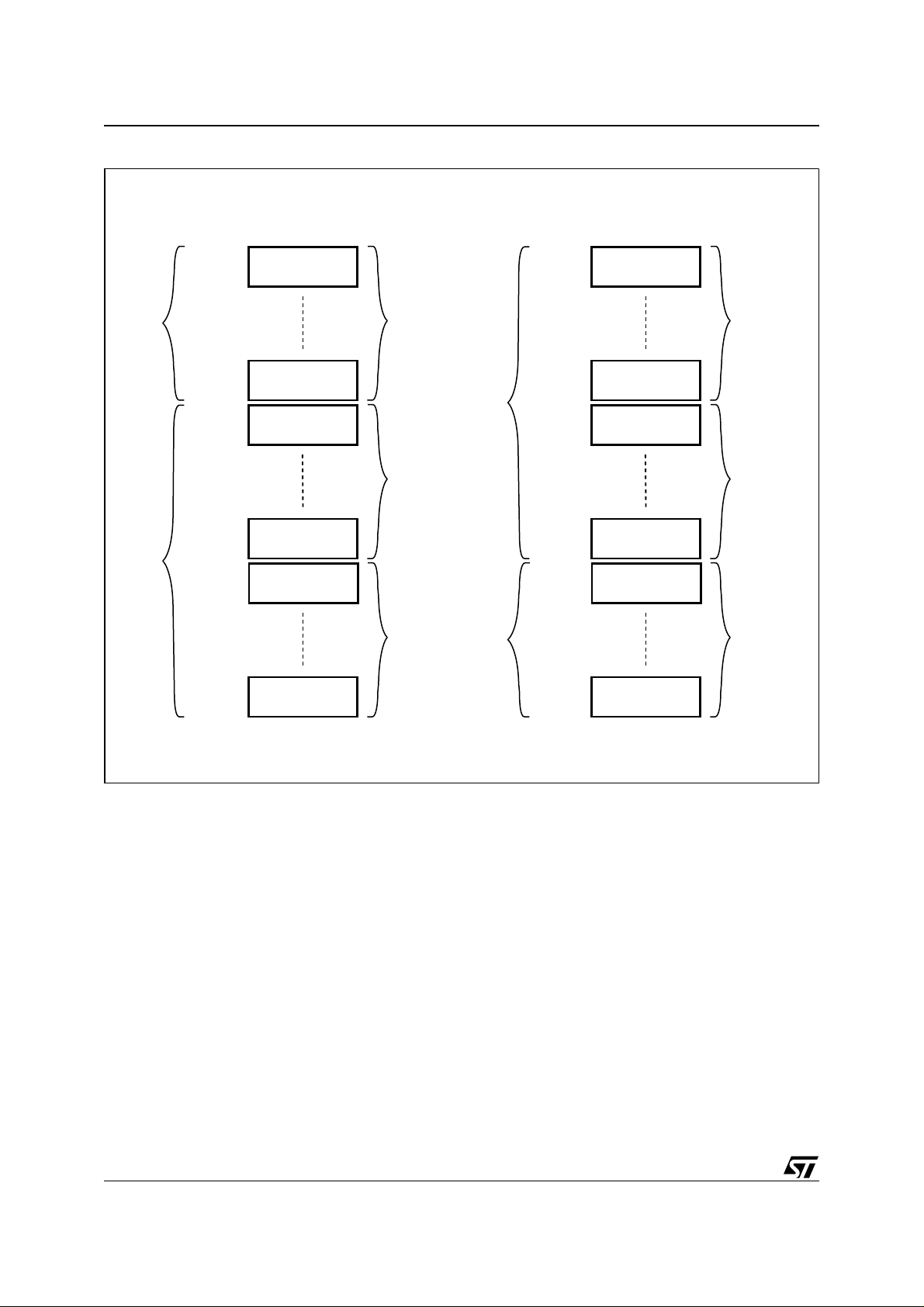
Table 5. Commands, 16-bit mode, BYTE
Table 6. Commands, 8-bit mode, BYTE
Table 7. Program, Erase Times and Program, Erase Endurance Cycles . . . . . . . . . . . . . . . . . . . 18
STATUS REGISTER . . . . . . . . . . . . . . . . . . . . . . . . . . . . . . . . . . . . . . . . . . . . . . . . . . . . . . . . . . . . . . . 19
= VIH. . . . . . . . . . . . . . . . . . . . . . . . . . . . . . . . . . . . . . . 17
= VIL. . . . . . . . . . . . . . . . . . . . . . . . . . . . . . . . . . . . . . . . 18
Data Polling Bit (DQ7). . . . . . . . . . . . . . . . . . . . . . . . . . . . . . . . . . . . . . . . . . . . . . . . . . . . . . . . . . . 19
Toggle Bit (DQ6).. . . . . . . . . . . . . . . . . . . . . . . . . . . . . . . . . . . . . . . . . . . . . . . . . . . . . . . . . . . . . . . 19
Error Bit (DQ5). . . . . . . . . . . . . . . . . . . . . . . . . . . . . . . . . . . . . . . . . . . . . . . . . . . . . . . . . . . . . . . . . 19
Erase Timer Bit (DQ3). . . . . . . . . . . . . . . . . . . . . . . . . . . . . . . . . . . . . . . . . . . . . . . . . . . . . . . . . . . 19
Alternative Toggle Bit (DQ2).. . . . . . . . . . . . . . . . . . . . . . . . . . . . . . . . . . . . . . . . . . . . . . . . . . . . . . 19
Table 8. Status Register Bits . . . . . . . . . . . . . . . . . . . . . . . . . . . . . . . . . . . . . . . . . . . . . . . . . . . . . 20
Figure 7. Data Polling Flowchart. . . . . . . . . . . . . . . . . . . . . . . . . . . . . . . . . . . . . . . . . . . . . . . . . . . 20
Figure 8. Toggle Flowchart. . . . . . . . . . . . . . . . . . . . . . . . . . . . . . . . . . . . . . . . . . . . . . . . . . . . . . . 20
DUAL OPERATIONS AND MULTIPLE BANK ARCHITECTURE . . . . . . . . . . . . . . . . . . . . . . . . . . . . 21
Table 9. Dual Operations Allowed In the Other Bank . . . . . . . . . . . . . . . . . . . . . . . . . . . . . . . . . . 21
Table 10. Dual Operations Allowed In Same Bank . . . . . . . . . . . . . . . . . . . . . . . . . . . . . . . . . . . . . 21
MAXIMUM RATING. . . . . . . . . . . . . . . . . . . . . . . . . . . . . . . . . . . . . . . . . . . . . . . . . . . . . . . . . . . . . . . . 22
Table 11. Absolute Maximum Ratings. . . . . . . . . . . . . . . . . . . . . . . . . . . . . . . . . . . . . . . . . . . . . . . 22
DC and AC PARAMETERS . . . . . . . . . . . . . . . . . . . . . . . . . . . . . . . . . . . . . . . . . . . . . . . . . . . . . . . . . 23
Table 12. Operating and AC Measurement Conditions. . . . . . . . . . . . . . . . . . . . . . . . . . . . . . . . . . 23
Figure 9. AC Measurement I/O Waveform . . . . . . . . . . . . . . . . . . . . . . . . . . . . . . . . . . . . . . . . . . . 23
Figure 10.AC Measurement Load Circuit . . . . . . . . . . . . . . . . . . . . . . . . . . . . . . . . . . . . . . . . . . . . 23
Table 13. Device Capacitance. . . . . . . . . . . . . . . . . . . . . . . . . . . . . . . . . . . . . . . . . . . . . . . . . . . . . 23
Table 14. DC Characteristics. . . . . . . . . . . . . . . . . . . . . . . . . . . . . . . . . . . . . . . . . . . . . . . . . . . . . . 24
Figure 11.Read Mode AC Waveforms. . . . . . . . . . . . . . . . . . . . . . . . . . . . . . . . . . . . . . . . . . . . . . . 25
Table 15. Read AC Characteristics . . . . . . . . . . . . . . . . . . . . . . . . . . . . . . . . . . . . . . . . . . . . . . . . .25
Figure 12.Write AC Waveforms, Write Enable Controlled. . . . . . . . . . . . . . . . . . . . . . . . . . . . . . . . 26
Table 16. Write AC Characteristics, Write Enable Controlled . . . . . . . . . . . . . . . . . . . . . . . . . . . . . 26
Figure 13.Write AC Waveforms, Chip Enable Controlled . . . . . . . . . . . . . . . . . . . . . . . . . . . . . . . . 27
3/50

M29DW323DT, M29DW323DB
Table 17. Write AC Characteristics, Chip Enable Controlled. . . . . . . . . . . . . . . . . . . . . . . . . . . . . . 27
Figure 14.Toggle and Alternative Toggle Bits Mechanism, Chip Enable Controlled. . . . . . . . . . . . 28
Figure 15.Toggle and Alternative Toggle Bits Mechanism, Output Enable Controlled . . . . . . . . . . 28
Table 18. Toggle and Alternative Toggle Bits AC Characteristics. . . . . . . . . . . . . . . . . . . . . . . . . . 28
Figure 16.Reset/Block Temporary Unprotect AC Waveforms. . . . . . . . . . . . . . . . . . . . . . . . . . . . . 29
Table 19. Reset/Block Temporary Unprotect AC Characteristics . . . . . . . . . . . . . . . . . . . . . . . . . . 29
Figure 17.Accelerated Program Timing Waveforms . . . . . . . . . . . . . . . . . . . . . . . . . . . . . . . . . . . . 29
PACKAGE MECHANICAL . . . . . . . . . . . . . . . . . . . . . . . . . . . . . . . . . . . . . . . . . . . . . . . . . . . . . . . . . . 30
Figure 18.TSOP48 Lead Plastic Thin Small Outline, 12x20 mm, Bottom View Package Outline . . 30
Table 20. TSOP48 Lead Plastic Thin Small Outline, 12x20 mm, Package Mechanical Data . . . . . 30
Figure 19.TFBGA48 6x8mm - 6x8 Ball Array, 0.8mm Pitch, Bottom View Package Outline. . . . . . 31
Table 21. TFBGA48 6x8mm - 6x8 Ball Array, 0.8mm Pitch, Package Mechanical Data. . . . . . . . . 31
PART NUMBERING . . . . . . . . . . . . . . . . . . . . . . . . . . . . . . . . . . . . . . . . . . . . . . . . . . . . . . . . . . . . . . . 32
Table 22. Ordering Information Scheme . . . . . . . . . . . . . . . . . . . . . . . . . . . . . . . . . . . . . . . . . . . . . 32
APPENDIX A.BLOCK ADDRESSES . . . . . . . . . . . . . . . . . . . . . . . . . . . . . . . . . . . . . . . . . . . . . . . . . . 33
Table 23. Top Boot Block Addresses, M29DW323DT. . . . . . . . . . . . . . . . . . . . . . . . . . . . . . . . . . . 33
Table 24. Bottom Boot Block Addresses, M29DW323DB . . . . . . . . . . . . . . . . . . . . . . . . . . . . . . . . 36
APPENDIX B.COMMON FLASH INTERFACE (CFI) . . . . . . . . . . . . . . . . . . . . . . . . . . . . . . . . . . . . . . 39
Table 25. Query Structure Overview . . . . . . . . . . . . . . . . . . . . . . . . . . . . . . . . . . . . . . . . . . . . . . . .39
Table 26. CFI Query Identification String. . . . . . . . . . . . . . . . . . . . . . . . . . . . . . . . . . . . . . . . . . . . .39
Table 27. CFI Query System Interface Information. . . . . . . . . . . . . . . . . . . . . . . . . . . . . . . . . . . . . 40
Table 28. Device Geometry Definition . . . . . . . . . . . . . . . . . . . . . . . . . . . . . . . . . . . . . . . . . . . . . .40
Table 29. Primary Algorithm-Specific Extended Query Table . . . . . . . . . . . . . . . . . . . . . . . . . . . . . 41
Table 30. Security Code Area . . . . . . . . . . . . . . . . . . . . . . . . . . . . . . . . . . . . . . . . . . . . . . . . . . . . . 41
APPENDIX C.EXTENDED MEMORY BLOCK . . . . . . . . . . . . . . . . . . . . . . . . . . . . . . . . . . . . . . . . . . . 42
Factory Locked Extended Block . . . . . . . . . . . . . . . . . . . . . . . . . . . . . . . . . . . . . . . . . . . . . . . . . 42
Customer Lockable Extended Block . . . . . . . . . . . . . . . . . . . . . . . . . . . . . . . . . . . . . . . . . . . . . . 42
Table 31. Extended Block Address and Data . . . . . . . . . . . . . . . . . . . . . . . . . . . . . . . . . . . . . . . . . 42
APPENDIX D.BLOCK PROTECTION. . . . . . . . . . . . . . . . . . . . . . . . . . . . . . . . . . . . . . . . . . . . . . . . . . 43
Programmer Technique . . . . . . . . . . . . . . . . . . . . . . . . . . . . . . . . . . . . . . . . . . . . . . . . . . . . . . . . 43
In-System Technique . . . . . . . . . . . . . . . . . . . . . . . . . . . . . . . . . . . . . . . . . . . . . . . . . . . . . . . . . . 43
Table 32. Programmer Technique Bus Operations, BYTE
= VIH or V
IL . . . . . . . . . . . . . . . . . . . . . . . . . . . 43
Figure 20.Programmer Equipment Group Protect Flowchart . . . . . . . . . . . . . . . . . . . . . . . . . . . . . 44
Figure 21.Programmer Equipment Chip Unprotect Flowchart. . . . . . . . . . . . . . . . . . . . . . . . . . . . . 45
Figure 22.In-System Equipment Group Protect Flowchart . . . . . . . . . . . . . . . . . . . . . . . . . . . . . . . 46
Figure 23.In-System Equipment Chip Unprotect Flowchart . . . . . . . . . . . . . . . . . . . . . . . . . . . . . . 47
REVISION HISTORY. . . . . . . . . . . . . . . . . . . . . . . . . . . . . . . . . . . . . . . . . . . . . . . . . . . . . . . . . . . . . . . 48
Table 33. Document Revision History . . . . . . . . . . . . . . . . . . . . . . . . . . . . . . . . . . . . . . . . . . . . . . . 48
4/50
SUMMARY DESCRIPTION
The M29DW323D is a 32 Mbit (4Mb x8 or 2Mb
x16) non-volatile memory that can be read, erased
and reprogrammed. These operations can be performed using a single low voltage (2.7 to 3.6V)
supply. On power-up the memory defaults to its
Read mode.
The device features an asymme trical block ar chitecture. The M29DW323D ha s an array of 8 parameter and 63 main blocks and is divided into two
Banks, A and B, providing D ual Bank o perations.
While programming or erasing in Bank A, read operations are possible in Bank B a nd vice versa.
Only one bank at a time is allo wed to be in program or erase mode. The bank architecture is
summariz ed in Table 2. M29DW323DT locates the
Parameter Blocks at the top of the memory address space whil e the M29 DW323DB locate s the
Parameter Blocks starting from the bottom.
M29DW323D has an extr a 32 KWord (x16 mode )
or 64 KByte (x8 mode) block, the Extended Block,
that can be accessed using a dedicated command. The Extended Block c an be protected and
so is useful fo r storing security in formation . How-
M29DW323DT, M29DW323DB
ever the protection is irreversible, o nce protected
the protection cannot be undone.
Each block can be eras ed independently so it is
possible to prese rve valid data while old data i s
erased. The blocks can be protected to prevent
accidental Program or Erase commands from
modifying the memory. Program and Erase com mands are written to the Command Interface of
the memory. An on-chip Program/Erase Controller
simplifies the proces s of programming or e rasing
the memory by taking care of all of the special operations that are required to upd ate the memory
contents. The end of a program or erase operation
can be detected an d any error conditions identified. The command set required to control the
memory is consistent with JEDEC standards.
Chip Enable, Output Enable and Write Enable signals control the bus operation of the memory.
They allow simple connection to most microprocessors, often without additional logic.
The memory is offered i n TSOP48 (12x20mm), and
TFBGA48 (6x8mm, 0.8mm pitch) packages. The
memory is supplied with all the bits erased (set to
’1’).
Figure 2. Logic Diagram Table 1. Signal Names
A0-A20 Address Inputs
DQ0-DQ7 Data Inputs/Outputs
VPP/WP
V
A0-A20
W
RP
CC
21
E
G
M29DW323DT
M29DW323DB
V
SS
15
DQ0-DQ14
DQ15A–1
BYTE
RB
AI05523
DQ8-DQ14 Data Inputs/Outputs
DQ15A–1 Data Input/Output or Address Input
E
G
W
RP
RB
BYTE
V
CC
VPP/WP
V
SS
NC Not Connected Inter na lly
Chip Enable
Output Enable
Write Enable
Reset/Block Temporary Unprotect
Ready/Busy Output
Byte/Word Organization Select
Supply Voltage
VPP/Write Protect
Ground
5/50
M29DW323DT, M29DW323DB
Figure 3. TSOP Connections
A15
1
48
A14
A13
A12
A11
A10 DQ14
A9
A8
A19
A20
M29DW323DT
M29DW323DB
W
RP
NC
12
13
37
36
VPP/WP
RB
A18
A17
A7
A6
A5
A4
A3
A2
A1
24 25
A16
BYTE
V
SS
DQ15A–1
DQ7
DQ6
DQ13
DQ5
DQ12
DQ4
V
CC
DQ11
DQ3
DQ10
DQ2
DQ9
DQ1
DQ8
DQ0
G
V
SS
E
A0
6/50
AI05524
Figure 4. TFBGA48 Connections (Top view through package)
M29DW323DT, M29DW323DB
654321
A
B
C
D
E
F
G
H
A3
A4
A2
A1
A0
E
G
V
SS
A7
A17
A6
A5 A20
DQ0
DQ8
DQ9
DQ1
RB
V
PP
A18
DQ2
DQ10
DQ11
DQ3
/
WP
W
RP
NC
A19
DQ5
DQ12
V
CC
DQ4
A9
A8
A10
A11
DQ7
DQ14
DQ13
DQ6
A13
A12
A14
A15
A16
BYTE
DQ15
A–1
V
SS
Table 2. Bank Architecture
Bank Bank Size
A 8 Mbit 8 8KByte/ 4 KWord 15 64KByte/ 32 KWord
B 24 Mbit - 48 64KByte/ 32 KWord
AI08084
Parameter Blocks Main Blocks
No. of Blocks Block Size No. of Blocks Block Size
7/50
M29DW323DT, M29DW323DB
Figure 5. Block Addresses (x8)
Bank B
Bank A
Top Boot Block (x8)
Address lines A20-A0, DQ15A-1
000000h
00FFFFh
2F0000h
2FFFFFh
300000h
30FFFFh
3E0000h
3EFFFFh
3F0000h
3F1FFFh
64 KByte or
32 KWord
64 KByte or
32 KWord
64 KByte or
32 KWord
64 KByte or
32 KWord
8 KByte or
4 KWord
Total of 48
Main Blocks
Total of 15
Main Blocks
Total of 8
Parameter
(1)
Blocks
Bank A
Bank B
Bottom Boot Block (x8)
Address lines A20-A0, DQ15A-1
000000h
001FFFh
00E000h
00FFFFh
010000h
01FFFFh
0F0000h
0FFFFFh
100000h
10FFFFh
8 KByte or
4 KWord
8 KByte or
4 KWord
64 KByte or
32 KWord
64 KByte or
32 KWord
64 KByte or
32 KWord
Total of 8
Parameter
(1)
Blocks
Total of 15
Main Blocks
Total of 48
Main Blocks
3FE000h
3FFFFFh
Note 1. Used as Extended Block Addresses in Extended Block mode.
Note: Also see APPENDIX A., Table 23. and Table 24. for a full listing of the Block Addresses.
8 KByte or
4 KWord
3F0000h
3FFFFFh
64 KByte or
32 KWord
AI05556
8/50
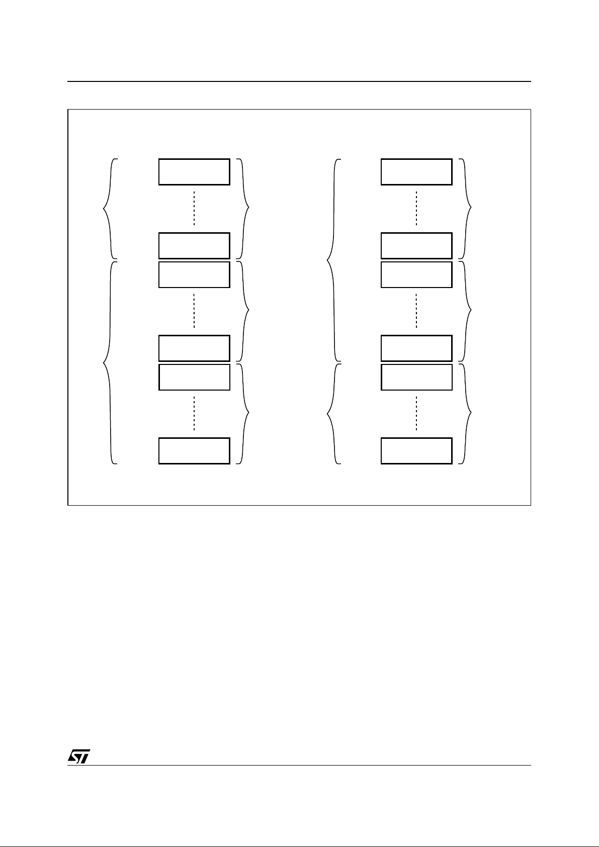
Figure 6. Block Addresses (x16)
M29DW323DT, M29DW323DB
Bank B
Bank A
000000h
007FFFh
178000h
17FFFFh
180000h
187FFFh
1F0000h
1F7FFFh
1F8000h
1F8FFFh
Top Boot Block (x16)
Address lines A20-A0
64 KByte or
32 KWord
64 KByte or
32 KWord
64 KByte or
32 KWord
64 KByte or
32 KWord
8 KByte or
4 KWord
Total of 48
Main Blocks
Total of 15
Main Blocks
Total of 8
Parameter
(1)
Blocks
Bank A
Bank B
000000h
000FFFh
007000h
007FFFh
008000h
00FFFFh
078000h
07FFFFh
080000h
087FFFh
Bottom Boot Block (x16)
Address lines A20-A0
8 KByte or
4 KWord
8 KByte or
4 KWord
64 KByte or
32 KWord
64 KByte or
32 KWord
64 KByte or
32 KWord
Total of 8
Parameter
(1)
Blocks
Total of 15
Main Blocks
Total of 48
Main Blocks
1FF000h
1FFFFFh
Note 1. Used as Extended Block Addresses in Extended Block mode.
Note: Also see APPENDIX A., Table 23. and Table 24. for a full listing of the Block Addresses.
8 KByte or
4 KWord
1F8000h
1FFFFFh
64 KByte or
32 KWord
AI05555
9/50

M29DW323DT, M29DW323DB
SIGNAL DESCRIPTIONS
See Figure 2., Logic Diagram, and Table
1., Signal Names, for a brief overview of the s ig-
nals connected to this device. Address Inputs (A0-A20). The Address Inputs
select the cells in the memory array to access during Bus Read operations. During Bus Write operations they control the commands sent to the
Command Interface of the Program/Erase Controller.
Data Inputs/Outputs (DQ0-DQ7). The Data I/O outputs the data stored at the selected address during a Bus Read operation. During Bus Write operations they repr esent the commands s ent to the Command Interface of the Program/Erase Controller.
Data Inputs/Outputs (DQ8-DQ14). The Data I/O outputs the data stored at the selected address during a Bus Read operati on wh en B YTE V
. When BYTE is Low, VIL, these pins are not
IH
used and are hig h impedance. During Bus W rite
operations the Command Regis ter does not use
these bits. When reading the Status Register
these bits should be ignored.
Data Input/Output or Address Input (DQ15A –1).
When BYTE
is High, VIH, this pin behaves as a
Data Input/Output pin (as DQ8-DQ14). When
BYTE
is Low, VIL, this pin behaves as an address
pin; DQ15A–1 Low will select the LSB of the addressed Word, DQ15A–1 High will select the MSB.
Throughout the text consider references to the
Data Input/Output to include this pin when BYTE
High and references to t he Address Inputs to include this pin when BYTE
is Low except when
stated explicitly otherwise.
Chip Enable (E
). The Chip Enable, E, activates
the memory, allowing Bus Read and Bus Write operations to be performed. When Chip Enable is
High, V
Output Enable (G
, all other pins are ignored.
IH
). The Output Enable, G, con-
trols the Bus Read operation of the memory.
Write Enable (W
). The Write Enabl e, W, controls
the Bus Write operation of the memory’s Command Interface.
V
Write Protect (VPP/WP). The VPP/Write
PP/
Protect
pin provides two functions. The VPP function allows the memory to use an external high
voltage power supply to reduce the time required
for Program operations. This is achieved by bypassing the unlock cycles and/o r using the Double Word or Quadruple Byte Program commands.
The Write Protect function provides a hardware
method of protecting the two outermost boot
blocks.
When V
/Write Protect is Low, VIL, the memory
PP
protects the two o utermost boot block s; Program
is High,
is
and Erase operations i n these bl ocks are ign ored
while V
at V
When V
/Write Protect is Low, even when RP is
PP
.
ID
/Write Protect is High, VIH, the memory
PP
reverts to the previous protection status of the two
outermost boot blocks. Program and Erase operations ca n now mod ify th e data in these blocks unless the blocks are protected using Block
Protection.
When V
/Write Protect is raised to V
PP
the mem-
PP
ory automatically enters the Unlock Bypass mode.
When V
/Write Protect returns to VIH or VIL nor-
PP
mal operation resumes. During Unlock Bypass
Program operations th e memory draws I
PP
from
the pin to supply the programming circuits. See the
description of the Unl ock By pas s c omm and in the
Command Interface sec tion. The transitio ns from
V
to VPP and from VPP to VIH must be slower
IH
than t
Never raise V
, see Figure 17.
VHVPP
/Write Protect to VPP from any
PP
mode except Read mode, otherwise the memory
may be left in an indeterminate state.
The V
/Write Protect pin must not be left floating
PP
or unconnected or the device may become unreliable. A 0.1µF capacitor should be connected between the V
/Write Protect pin and the V
PP
SS
Ground pin to decouple the current surges from
the power supply. The PCB track widths must be
sufficient to carry the currents required during
Unlock Bypass Program, I
Reset/Block Temporary Unprotect (RP
PP
.
). The
Reset/Block Temporary Unprotect pin can be
used to apply a Hardware Reset to the memory or
to temporarily unprote ct all Bl oc ks t hat h av e be en
protected.
Note that if V
/WP is at VIL, then the two outer-
PP
most boot blocks will remain protected even if RP
is at V
ID
.
A Hardware Reset is achieved by holdi ng Reset/
Block Temporary Unp rotect Low, V
. After Reset/Block Temporary Unprotect
t
PLPX
goes High, V
, the memory will be ready f or Bus
IH
Read and Bus Write operations after t
, whichever occurs last. See the Ready/Busy
t
RHEL
, for at least
IL
PHEL
or
Output section, Tabl e 19. and Figure 16., Reset/
Block Temporary Unprotect AC Waveforms, for
more details.
Holding RP
at VID will temporarily unprotect the
protected Blocks in the memory. Program and
Erase operations on all blocks will be possible.
The transition from V
PHPHH
.
t
Ready/Busy Output (RB
to VID must be slower than
IH
). The Ready/Busy pin
is an open-drain output that can be used to identify
when the device is performing a Program or Erase
10/50

M29DW323DT, M29DW323DB
operation. During Program or Erase operations
Ready/Busy is Low, V
. Ready/Busy is hig h-im-
OL
pedance during Read mode, Auto Select mode
and Erase Suspend mode.
After a Hardware Reset, Bus Read and Bus Write
operations cannot begin until Ready/Busy becomes high-impedance. See Table 19. and Figure
16., Reset/Block Tempor ary Unpro tect AC Wa veforms.
The use of an open-drain output allows the Ready/
Busy pins from several memories to be connected
to a single pull-up resistor. A Low will then indicate
that one, or more, of the memories is busy.
Byte/Word Organizatio n Select (BYTE
). The
Byte/Word Organization Select pin is used to
switch between the x8 and x16 Bus modes of the
memory. When Byte/ Word Organi zation Sel ect is
Low, V
High, V
, the memory is in x8 mode, when it is
IL
, the memory is in x16 mode.
IH
Supply Voltage (2.7V to 3.6V). VCC pro-
V
CC
vides the power su pply for all operations (Read,
Program and Erase).
The Command Interface is disabled when the V
CC
Supply Voltage is le ss than the Lockout Vo ltage,
V
. This prevents Bus Write operations from ac-
LKO
cidentally damaging the data during power up,
power down and power surges. If the Program/
Erase Controller is programming or erasing during
this time then the operation aborts and the memory contents being altered will be invalid.
A 0.1µF capacito r should be connected between
the V
Supply Voltage pin and the VSS Ground
CC
pin to decouple the current surges from the power
supply. The PCB track widths must be sufficient to
carry the currents required during Program and
Erase operations, I
Ground. VSS is the referenc e for all voltage
V
SS
measurements. The d evic e fe atures tw o V
CC3
.
pins
SS
which must be both connected to the system
ground.
11/50

M29DW323DT, M29DW323DB
BUS OPERATIONS
There are five standard bus operations that control
the device. These are Bus Read, Bus Writ e, Output Disable, Standby and Automatic Standby.
The Dual Bank architectu re of the M 29DW32 3 allows read/write operations in Bank A, while read
operations are being e xecuted in Bank B or vice
versa. Write operations are only allowed in one
bank at a time.
See Tables 3 and 4, Bus Operations, for a summary. Typically glitche s of les s than 5ns on Chip Enable or Write Ena ble are ignored by t he memory
and do not affect bus operations.
Bus Read. Bus Read operations read from the memory cells, or specific registers in the Command Interface. A valid Bus Read operation involves setting the desired address on the Address Inputs, applying a Low s ig nal, V and Output Enable and keeping Write Enable High, V
. The Data Inputs/Outputs will ou tpu t the
IH
value, see Figure 11., Read Mode AC Waveforms,
and Table 15., Read AC Characteristics, for details of when the output becomes valid.
Bus Write. Bus Write operations write to the Command Interface. A v alid Bus Write operati on begins by setting the desired address on the Address Inputs. The Ad dress Inputs are latched b y the Command Interface on the falling edge of Chip Enable or Write Enable, whichever occurs last. The Data Inputs/Outputs ar e latched by the Com mand Interface on the rising ed ge of Chip Enab le or Write Enable, whichever occurs first. Output Enable must remain High, V
IH
Write operation. See Figures 12 and 13, Write AC
Waveforms, and Tables 16 and 17, Write AC
Characteristics, for details of the timing requirements.
Output Disable. The Data Inputs/Outpu ts are in the high impedance state when Output Enable is High, V
.
IH
Standby. When Chip Enable is High, V memory enters Standby mode and the Data Inputs/Outputs pins are placed in the high-imped-
, to Chip Enable
IL
, during the whole Bus
, the
IH
ance state. To reduce the Su pply Current to the
Standby Supply Current, I
be held within V
± 0.2V. For the Standby current
CC
, Chip Enable should
CC2
level see Table 14., DC Characteristics.
During program or eras e operations the memory
will continue to use the Program/Erase Supply
Current, I
, for Program or Erase operations un-
CC3
til the operation completes. Automatic Standby. If CMOS levels (V
± 0.2V)
CC
are used to drive the bus and the bus is inactive for
300ns or more the memory enters Automatic
Standby where the interna l Supply Current is reduced to the Standby Supply Current, I
CC2
. The
Data Inputs/Outputs will still output data if a Bus
Read operation is in progress.
Special Bus Operations
Additional bus operations can be performed to
read the Electronic Signature and also to apply
and remove Block Protection. These bus operations are intended for us e by progr ammin g equip ment and are not usually used in applications.
They require V
to be applied to some pins.
ID
Electronic Signature. The memory has two codes, the manufacturer code and the device code, that can be read to identify the memory. These codes can b e read b y apply ing the sig nals listed in Tables 3 and 4, Bus Operations.
Block Protect and Chip Unprotect.
Groups of
blocks can be protected against accidental Program or Erase. The Prot ection Groups are sh own
in APPENDIX A., Tables 23 and 24, Block Addresses. The whole chip can be unprotected to allow the data inside the blocks to be changed.
The V
the two outermost boot blocks. When V
Protect
/Write Protect pin can be used to protect
PP
is at V
the two outermost boot blocks are
IL
PP
/Write
protected and remain protected regardless of the
Block Protection Status or the Reset/Block Temporary Unprotect pin status.
Block Protect an d Chip Unprotect ope rations are
described in APPENDIX D.
12/50
M29DW323DT, M29DW323DB
Table 3. Bus Operations, BYTE = V
Operation E G W
Bus Read
Bus Write
Output Disable X
Standby
Read Manufacturer
Code
Read Device Code
Extended Memory
Block Verify Code
Note: X = VIL or VIH.
V
V
V
V
V
V
V
IL
IL
IH
IL
IL
IL
IL
V
IH
V
IH
X X X Hi-Z Hi-Z
V
IL
V
IL
V
IL
Table 4. Bus Operations, BYTE = V
Operation E
Bus Read
Bus Write
Output Disable X
Standby
Read Manufacturer
Code
Read Device Code
Extended Memory
Block Verify Code
Note: X = VIL or VIH.
V
V
V
V
V
V
G W
V
IL
IL
IH
IL
IL
IL
IL
V
IH
V
IH
XXX Hi-Z
V
IL
V
IL
V
IL
IL
Address Inputs
DQ15A–1, A0-A2 0
V
Cell Address Hi-Z Data Output
IH
V
Command Address Hi-Z Data Input
IL
V
X Hi-Z Hi-Z
IH
A0 = VIL, A1 = VIL, A9 = VID,
V
IH
Others V
A0 = VIH, A1 = VIL,
V
IH
A9 = V
A0 = VIH, A1 = VIH, A6 = VIL,
V
IH
A9 = V
IH
or V
IL
IH
, Others VIL or V
ID
, Others VIL or V
ID
DQ14-DQ8 DQ7-DQ0
IH
IH
Address Inputs
A0-A20
V
Cell Address Data Output
IH
V
Command Address Data Input
IL
V
XHi-Z
IH
A0 = VIL, A1 = VIL, A9 = VID,
V
IH
Others VIL or V
A0 = VIH, A1 = VIL, A9 = VID,
V
IH
Others VIL or V
A0 = VIH, A1 = VIH, A6 = VIL,
V
IH
A9 = V
ID
IH
IH
, Others VIL or V
IH
Data Inputs/Outp uts
Hi-Z 20h
Hi-Z
Hi-Z
5Eh (M29DW323DT)
5Fh (M29DW323D B)
81h (factory locked)
01h (not factory locked)
Data Inputs/Outputs
DQ15A–1, DQ14-DQ0
0020h
225Eh (M29DW323DT)
225Fh (M29DW323DB)
81h (factory locked)
01h (not factory locked)
13/50

M29DW323DT, M29DW323DB
COMMAND INTERFACE
All Bus Write operations to the memory are interpreted by the Command Interface. Commands
consist of one or more sequential Bus Write operations. Failure to observe a valid sequence of Bus
Write operation s will result in the memory return ing to Read mode. The long command sequences
are imposed to maximize data security.
The address used for the commands changes depending on whether the memory is in 16-bit or 8bit mode. See either Table 5, or 6, depending on
the configuration that is being used, for a summary
of the commands.
Read/Reset Command
The Read/Reset command returns the memory to
its Read mode. It also resets the errors in the Status Register. Either one or three Bus Wr i te ope ra tions can be used to issue the Read/Reset
command.
The Read/Reset command can be issued, between Bus Write cycles before the start of a program or erase operation, to return the device to
read mode. If the Read/Reset command is issu ed
during the time-out of a Block erase operation then
the memory will take up to 10µ s to abort. During
the abort period no valid data can be read from the
memory. The Read/Reset command will not abort
an Erase operation when issued while in Erase
Suspend.
Auto Select Command
The Auto Select command is used to read the
Manufacturer Code, th e Device Code, the Block
Protection Status and the Extended Memory Block
Verify Code. It can be addressed to either Bank.
Three consecutive Bus Write operations are required to issue the Auto Sel ect command. Th e final Write cycle must be addressed to one of the
Banks. Once th e Auto Sele ct comm and is issu ed
Bus Read operations to the Bank where the command was issued output the Auto Select data. Bus
Read operations to the other Bank will outpu t the
contents of the memory array. The memory remains in Auto Select mode until a Read/Reset or
CFI Query command is issued.
In Auto Select mode the M anufacturer Code can
be read using a Bus Read operation with A0 = V
and A1 = VIL and A19-A20 = B ank Address. The
other address bits may be set to either V
The Device Code ca n be read using a Bu s Read
operation with A0 = V
and A1 = VIL and A19-A20
IH
= Bank Address. The other address bits may be
set to either V
or VIH.
IL
The Block Protectio n Statu s of ea ch block c an be
read using a Bus Read ope ration with A0 = V
A1 = V
, A19-A20 = Bank Address and A12-A 18
IH
specifying the address of the block inside the
or VIH.
IL
IL
Bank. The other address bits ma y be set to eithe r
V
or VIH. If the addressed block is protected then
IL
01h is output on Data Inputs/Ou tputs DQ0-DQ7,
otherwise 00h is output.
Read CFI Query Command
The Read CFI Query Comma nd is used to read
data from the Common Flash Interface (CFI)
Memory Area. This command is valid when the device is in the Read Array mode, or when the device
is in Auto Select mode.
One Bus Write cycle is required to issue the Read
CFI Query Command . Once the command is issued subsequent Bus Read operatio ns read from
the Common Flash Interface Memory Area.
The Read/Reset command must be issue d to return the device to the previous mode (the Read Array mode or Aut o Select mode ). A second R ead/
Reset command would be needed if the d evice i s
to be put in the Read Array mode from Auto Select
mode.
See APPENDIX B. , Tables 25, 26, 27, 28, 29 and
30 for details on the informati on contained in the
Common Flash Interface (CFI) memory area.
Program Command
The Program command can be used to program a
value to one address in the memory array at a
time. The command requires four Bus Write op er ations, the final write operation latches the address and data, and starts the Program/Erase
Controller.
If the address falls in a protect ed block then the
Program command is ignored, the data remains
unchanged. The Status Register is never read and
no error condition is given.
During the program operation th e memory will ig nore all commands. It is no t possib le to is sue any
command to abort or pause the operation. After
programming has started, Bus Read operations in
the Bank being programmed output the Status
Register content, while Bus Read operations to
the other Bank output the contents of the memory
array. See the section on the Status Register for
more details. Typical program times are given in
Table 7.
IL
After the program operation has completed the
memory will return to the Read mode, unless an
error has occurred. When an error occurs Bus
Read operations to the Bank where the command
was issued will continue to output the Status Register. A Read/Reset command mus t be issued to
reset the error condition and return to Read mode.
Note that the Program command cannot change a
,
bit set at ’0’ back t o ’1’. One of the Erase Commands must be used to set all the bits in a block or
in the whole memory from ’0’ to ’1’.
14/50

M29DW323DT, M29DW323DB
Fast Program Commands
There are two Fast P rogr am c omm and s av ail ab le
to improve the programming throughput, by writing
several adjacent words or bytes in parallel. The
Quadruple Byte Program command is available for
x8 operations, while the Double Word Program
command is available for x16 operations.
Only one bank can be programmed at any one
time. The other bank must be in Read mode or
Erase Suspend.
Fast Program commands should not be attempted
when V
because applying a 12V V
pin will temporarily unprotect any protected
WP
WP is not at VPP. Care must be taken
PP/
voltage to the VPP/
PP
block.
After programming h as started, Bus R ead opera-
tions in the Bank being programmed output the
Status Register content, while Bus Read operations to the other Ban k output the cont ents of the
memory array.
After the program operation has completed the
memory will return to the Read mode, unless an
error has occurred. When an error occurs Bus
Read operations to the Bank where the command
was issued will continue to output the Status Register. A Read/Reset command mus t be issued to
reset the error condition and return to Read mode.
Note that the Fast Program commands cannot
change a bit set at ’0’ back to ’1’. One of the Erase
Commands must be us ed to set all the bits in a
block or in the whole memory from ’0’ to ’1’.
Typical Program times are given in Table
7., Program, Erase Times and Program, Erase
Endurance Cycles.
Quadruple Byte Program Command. The Quadruple Byte Program co mmand is used to wr ite a page of four adjacent Bytes in parallel. The four bytes must differ only for addresses A0, DQ15A-1. Five bus write cycles are necessary to issue the Quadruple Byte Program command.
■ The first bus cycle sets up the Quadruple Byte
Program Command.
■ The second bus cycle latches the Address and
the Data of the first byte to be written.
■ The third bus cycle latches the Address and
the Data of the second byte to be written.
■ The fourth bus cycle latches the Address and
the Data of the third byte to be written.
■ The fifth bus cycle latches the Address and the
Data of the fourth byte to be written and starts
the Program/Erase Controller.
Double Word Program Command. The Double Word Program com mand is used to write a page of two adjacent wor ds in parallel. The tw o words must differ only for the address A0.
Three bus write cy cles ar e ne ce ss ary to i ss ue the
Double Word Program command.
■ The first bus cycle sets up the Double Word
Program Command.
■ The second bus cycle latches the Address and
the Data of the first word to be written.
■ The third bus cycle latches the Address and
the Data of the second word to be written and
starts the Program/Erase Controller.
Unlock Bypass Command
The Unlock Bypass com mand is used in conju nction with the Unlock Bypass Program command to
program the memory faster than with the standard
program commands. W hen the cycle time to the
device is long, considerable time saving can be
made by using these commands. Three Bus Write
operations are required to issue the Unlock Bypass command.
Once the Unlock Bypass c ommand has been issued the bank enters Unlock Bypass mode. When
in Unlock Bypass mode, only the Unlock Bypass
Program and Unlock Bypass Reset commands
are valid. The Unlock Bypa ss Program co mmand
can be issued to program addresses within the
bank, and the Unlo ck Bypass Res et command to
return the bank to Read mode. In Unlock Byp ass
mode the m emory can be read as if i n Read mode .
When V
is applied to the VPP/Write Protect pin
PP
the memory automatica lly enters the Unlock Bypass mode and the Unlock Bypass Program command can be issued immediately. Care must be
taken because applying a 12V V
VPP/WP
pin will temporarily unprotect any protect-
voltage to the
PP
ed block.
Unlock Bypass Program Command
The Unlock Bypass Program command can be
used to program one address in the memory array
at a time. The command requires two Bus Write
operations, the final write operation latches the address and data, and starts the Program/Erase
Controller.
The Program operation us ing the Unlock Bypass
Program command behaves identically to the Program operation using the Program command. The
operation cannot be aborted, a Bus Read ope ration to the Bank where the command was is sued
outputs the Status Register. See the Program
command for details on the behavior.
Unlock Bypass Reset Command
The Unlock Bypass Re se t co mm and ca n be used
to return to Read/Reset mode from Unlock Bypass
Mode. Two Bus Write operations are required to
issue the Unlock B ypass Reset command. Re ad/
Reset command does not exit from Unlock Bypass
Mode.
15/50
 Loading...