

查询27C512供应商
512 Kbit (64K x8) UV EPROM and OTP EPROM
FEATURES SUMMARY
■ 5V ± 10% SUPPLY VOLTAGE in READ
OPERATION
■ ACCESS TIME: 45ns
■ LOW POWER “CMOS” CONSUMPTION:
– Active Current 30mA
– Standby Current 100µA
■ PROGRAMMI NG VOLTAGE: 12.75V ± 0.25V
■ PROGRAMMING TIMES of AROUND 6sec.
■ ELECTRONIC SIGNATURE
– Manufacturer Code: 20h
– Device Code: 3Dh
■ PACKAGES
– Lead-Free Versions
M27C512
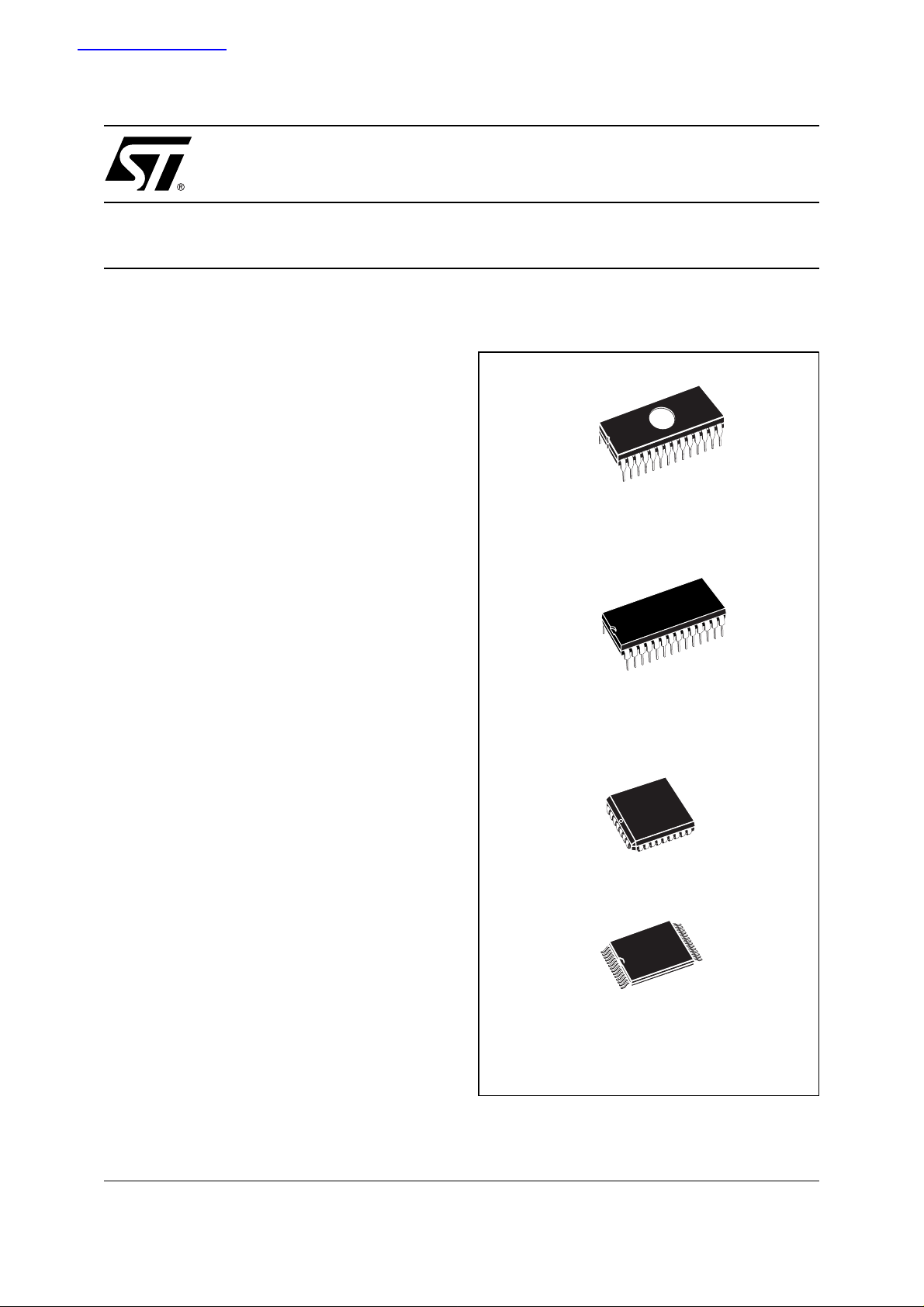
Figure 1. Packages
28
1
FDIP28W (F)
28
PLCC32 (C)
TSOP28 (N)
8 x 13.4 mm
1
PDIP28 (B)
1/22November 2004

M27C512
TABLE OF CONTENTS
FEATURES SUMMARY . . . . . . . . . . . . . . . . . . . . . . . . . . . . . . . . . . . . . . . . . . . . . . . . . . . . . . . . . . . . . 1
Figure 1. Packages. . . . . . . . . . . . . . . . . . . . . . . . . . . . . . . . . . . . . . . . . . . . . . . . . . . . . . . . . . . . . . 1
SUMMARY DESCRIPTION. . . . . . . . . . . . . . . . . . . . . . . . . . . . . . . . . . . . . . . . . . . . . . . . . . . . . . . . . . . 4
Figure 2. Logic Diagram . . . . . . . . . . . . . . . . . . . . . . . . . . . . . . . . . . . . . . . . . . . . . . . . . . . . . . . . . . 4
Table 1. Signal Names . . . . . . . . . . . . . . . . . . . . . . . . . . . . . . . . . . . . . . . . . . . . . . . . . . . . . . . . . . 4
Figure 3. DIP Connections . . . . . . . . . . . . . . . . . . . . . . . . . . . . . . . . . . . . . . . . . . . . . . . . . . . . . . . . 5
Figure 4. LCC Connections. . . . . . . . . . . . . . . . . . . . . . . . . . . . . . . . . . . . . . . . . . . . . . . . . . . . . . . . 5
Figure 5. TSOP Connections . . . . . . . . . . . . . . . . . . . . . . . . . . . . . . . . . . . . . . . . . . . . . . . . . . . . . . 5
DEVICE OPERATION . . . . . . . . . . . . . . . . . . . . . . . . . . . . . . . . . . . . . . . . . . . . . . . . . . . . . . . . . . . . . . . 6
Read Mode . . . . . . . . . . . . . . . . . . . . . . . . . . . . . . . . . . . . . . . . . . . . . . . . . . . . . . . . . . . . . . . . . . . . 6
Standby Mode . . . . . . . . . . . . . . . . . . . . . . . . . . . . . . . . . . . . . . . . . . . . . . . . . . . . . . . . . . . . . . . . . 6
Table 2. Operating Modes . . . . . . . . . . . . . . . . . . . . . . . . . . . . . . . . . . . . . . . . . . . . . . . . . . . . . . . . 6
Table 3. Electronic Signature. . . . . . . . . . . . . . . . . . . . . . . . . . . . . . . . . . . . . . . . . . . . . . . . . . . . . . 6
Two Line Output Control . . . . . . . . . . . . . . . . . . . . . . . . . . . . . . . . . . . . . . . . . . . . . . . . . . . . . . . . 6
System Considerations. . . . . . . . . . . . . . . . . . . . . . . . . . . . . . . . . . . . . . . . . . . . . . . . . . . . . . . . . . 6
Programming . . . . . . . . . . . . . . . . . . . . . . . . . . . . . . . . . . . . . . . . . . . . . . . . . . . . . . . . . . . . . . . . . . 7
Figure 6. Programming Flowchart. . . . . . . . . . . . . . . . . . . . . . . . . . . . . . . . . . . . . . . . . . . . . . . . . . . 7
PRESTO IIB Programming Algorithm . . . . . . . . . . . . . . . . . . . . . . . . . . . . . . . . . . . . . . . . . . . . . . 7
Program Inhibit . . . . . . . . . . . . . . . . . . . . . . . . . . . . . . . . . . . . . . . . . . . . . . . . . . . . . . . . . . . . . . . . 7
Program Verify. . . . . . . . . . . . . . . . . . . . . . . . . . . . . . . . . . . . . . . . . . . . . . . . . . . . . . . . . . . . . . . . . 7
Electronic Signature . . . . . . . . . . . . . . . . . . . . . . . . . . . . . . . . . . . . . . . . . . . . . . . . . . . . . . . . . . . . 7
ERASURE OPERATION (APPLIES FOR UV EPROM) . . . . . . . . . . . . . . . . . . . . . . . . . . . . . . . . . . . . . 8
MAXIMUM RATING. . . . . . . . . . . . . . . . . . . . . . . . . . . . . . . . . . . . . . . . . . . . . . . . . . . . . . . . . . . . . . . . . 9
Table 4. Absolute Maximum Ratings. . . . . . . . . . . . . . . . . . . . . . . . . . . . . . . . . . . . . . . . . . . . . . . . 9
DC and AC PARAMETERS . . . . . . . . . . . . . . . . . . . . . . . . . . . . . . . . . . . . . . . . . . . . . . . . . . . . . . . . . 10
Table 5. AC Measurement Conditions. . . . . . . . . . . . . . . . . . . . . . . . . . . . . . . . . . . . . . . . . . . . . . 10
Figure 7. Testing Input Output Waveform. . . . . . . . . . . . . . . . . . . . . . . . . . . . . . . . . . . . . . . . . . . . 10
Figure 8. AC Testing Load Circuit. . . . . . . . . . . . . . . . . . . . . . . . . . . . . . . . . . . . . . . . . . . . . . . . . . 10
Table 6. Capacitance. . . . . . . . . . . . . . . . . . . . . . . . . . . . . . . . . . . . . . . . . . . . . . . . . . . . . . . . . . . 10
Table 7. Read Mode DC Characteristics. . . . . . . . . . . . . . . . . . . . . . . . . . . . . . . . . . . . . . . . . . . . 11
Table 8. Read Mode AC Characteristics . . . . . . . . . . . . . . . . . . . . . . . . . . . . . . . . . . . . . . . . . . . . 11
Table 9. Read Mode AC Characteristics . . . . . . . . . . . . . . . . . . . . . . . . . . . . . . . . . . . . . . . . . . . . 12
Figure 9. Read Mode AC Waveforms. . . . . . . . . . . . . . . . . . . . . . . . . . . . . . . . . . . . . . . . . . . . . . . 12
Table 10. Programming Mode DC Characteristics . . . . . . . . . . . . . . . . . . . . . . . . . . . . . . . . . . . . . 13
Table 11. Margin Mode AC Characteristics. . . . . . . . . . . . . . . . . . . . . . . . . . . . . . . . . . . . . . . . . . . 14
Figure 10.Margin Mode AC Waveforms . . . . . . . . . . . . . . . . . . . . . . . . . . . . . . . . . . . . . . . . . . . . . 14
Table 12. Programming Mode AC Characteristics . . . . . . . . . . . . . . . . . . . . . . . . . . . . . . . . . . . . . 15
Figure 11.Programming and Verify Modes AC Waveforms. . . . . . . . . . . . . . . . . . . . . . . . . . . . . . . 15
2/22

M27C512
PACKAGE MECHANICAL . . . . . . . . . . . . . . . . . . . . . . . . . . . . . . . . . . . . . . . . . . . . . . . . . . . . . . . . . . 16
Figure 12.FDIP28W - 28 pin Ceramic Frit-seal DIP, with window, Package Outline. . . . . . . . . . . . 16
Table 13. FDIP28W - 28 pin Ceramic Frit-seal DIP, with window, Package Mechanical Data . . . . 16
Figure 13.PDIP28 - 28 pin Plastic DIP, 600 mils width, Package Outline . . . . . . . . . . . . . . . . . . . . 17
Table 14. PDIP28 - 28 pin Plastic DIP, 600 mils width, Package Mechanical Data . . . . . . . . . . . . 17
Figure 14.PLCC32 - 32 lead Plastic Leaded Chip Carrier, Package Outline . . . . . . . . . . . . . . . . . 18
Table 15. PLCC32 - 32 lead Plastic Leaded Chip Carrier, Package Mechanical Data . . . . . . . . . . 18
Figure 15.TSOP28 - 28 lead Plastic Thin Small Outline, 8 x 13.4 mm, Package Outline . . . . . . . . 19
Table 16. TSOP28 - 28 lead Plastic Thin Small Outline, 8 x 13.4 mm, Package Mechanical Data 19
PART NUMBERING . . . . . . . . . . . . . . . . . . . . . . . . . . . . . . . . . . . . . . . . . . . . . . . . . . . . . . . . . . . . . . . 20
Table 17. Ordering Information Scheme . . . . . . . . . . . . . . . . . . . . . . . . . . . . . . . . . . . . . . . . . . . . . 20
REVISION HISTORY. . . . . . . . . . . . . . . . . . . . . . . . . . . . . . . . . . . . . . . . . . . . . . . . . . . . . . . . . . . . . . . 21
Table 18. Revision History. . . . . . . . . . . . . . . . . . . . . . . . . . . . . . . . . . . . . . . . . . . . . . . . . . . . . . . . 21
3/22
M27C512
SUMMARY DESCRIPTION
The M27C512 is a 512 Kbit EPROM offered in the
two ranges UV (ultra vio let erase) and OTP (o ne
time programmable). It is ideally suited for applications where fast turn-around and pattern experimentation are important requirements and is
organized as 65536 by 8 bits.
The FDIP28W (window ceramic frit-seal package)
has transparent lid which allows the user to expose the chip to ultraviolet light to erase the bit pattern. A new pattern can then be written to the
device by following the programming procedure.
For applications where the content is programmed
only one time and erasure is not required, the
M27C512 is offered in PDIP28, PLCC32 and
TSOP28 (8 x 13.4 mm) packages.
In addition to the standard versions, the packages
are also available in Lead-free versions, in compliance with JEDEC Std J-STD-020 B, the ST ECOPACK 7191395 Specification, and the RoHS
(Restriction of Hazardous Substances) directive.
Figure 2. Logic Diagram
V
CC
16
A0-A15
GV
E
PP
M27C512
V
SS
8
Q0-Q7
AI00761B
Table 1. Signal Names
A0-A15 Address Inputs
Q0-Q7 Data Outputs
E
G
V
V
NC
DU
V
CC
SS
PP
Chip Enable
Output Enable / Progra m Sup pl y
Supply Voltage
Ground
Not Connected Internally
Don’t Use
4/22
M27C512
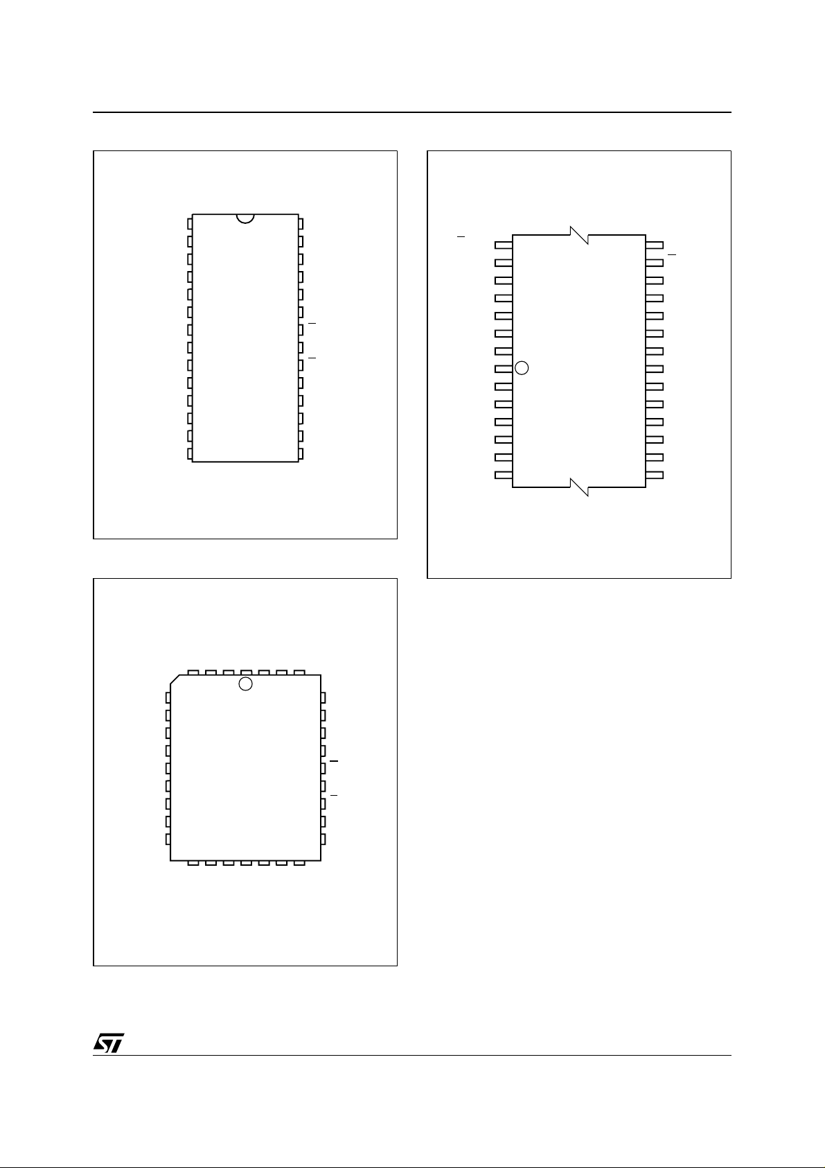
Figure 3. DIP Connections
1
A15 V
2
A12
A7
3
A6
4
A5
5
A4
6
A3
7
M27C512
8
A2
A1
9
A0
10
Q0
11
12
Q2
13
14
SS
28
27
26
25
24
23
22
21
20
19
18
17
16
15
AI00762
CC
A14
A13
A8
A9
A11
GV
A10
E
Q7
Q6
Q5Q1
Q4
Q3V
PP
Figure 5. TSOP Connections
GV
A11
A13
A14
V
A15
A12
PP
A9
A8
CC
A7
A6
A5
A4
A3
22
28
M27C512
1
78
21
15
14
AI00764B
A10
E
Q7
Q6
Q5
Q4
Q3
V
SS
Q2
Q1
Q0
A0
A1
A2
Figure 4. LCC Connections
A15
A6
A5
A4
A3
A2
A1
A0
NC
Q0
A7
9
Q1
DU
A12
1
M27C512
17
Q2
SS
DU
V
32
CC
V
Q3
A14
Q4
A13
25
Q5
A8
A9
A11
NC
GV
A10
E
Q7
Q6
AI00763
PP
5/22
M27C512
DEVICE OPERATION
The modes of operations of the M27C512 are listed in the Operating Modes table. A single power
supply is required in the read mode. All inputs are
TTL levels except for G
Electronic Signature.
Read Mode
The M27C512 has two cont rol functions, both of
which must be logically active in order to obtain
data at the outputs. Chip E nable (E
control and shou ld be used for device selecti on.
Output Enable (G
) is the output control and should
be used to gate data to the output pins, indepen dent of device selection. Assuming that the ad-
Table 2. Operating Modes
Mode E
Read
Output Disable
Program
Program Inhibit
Standby
Electronic Signature
Note: X = VIH or VIL, VID = 12V ± 0.5V.
VPP and 12V on A9 for
) is the power
V
IL
V
IL
VIL Pulse V
V
IH
V
IH
V
IL
dresses are stable, the address access time
(t
) is equal to the delay from E to output
AVQV
). Data i s availa ble at t he output after a delay
(t
ELQV
of t
has been low and the addresses have been sta-
E
ble for at least t
from the falling edge of G , as sumi ng that
GLQV
AVQV-tGLQV
.
Standby Mode
The M27C512 has a standby mode which reduces
the active current from 30mA to 100µA The
M27C512 is placed in the standby mode by applying a CMOS high signal to the E
input. When in the
standby mode, the outputs are in a high impedance state, independent of the G
GV
PP
V
IL
V
IH
PP
V
PP
XXHi-Z
V
IL
A9 Q7-Q0
X Data Out
XHi-Z
XData In
XHi-Z
V
ID
VPP input.
Codes
Table 3. Electronic Signature
Identifier A0 Q7 Q6 Q5 Q4 Q3 Q2 Q1 Q0 Hex Data
Manufacturer’s Code
Device Code
V
IL
V
IH
Two Line Output Control
Because EPROMs are usually used in larger
memory arrays, the product features a 2 line control function which accommodates the use of multiple memory connection. The two line control
function allows:
a. the lowest possible memory power
dissipation,
b. complete assurance that output bus
contention will not occur.
For the most efficient use of these two control
lines, E
should be decoded and used as the primary device selecting function, while G
made a common connect ion to all devices in the
array and connected to the READ
system control bus. This ensures that all deselected memory devices are in their low power standby
mode and that the output pins are only active
00100000 20h
00111101 3Dh
when data is required from a particular memory
device.
System Considerations
The power switch ing characteristics of Advanced
CMOS EPROMs require careful decoupling of the
devices. The supply c urrent, I
CC
ments that are of interest to the system desi gner:
the standby current level, th e active cu rrent le vel,
and transient current peak s that are produced b y
the falling and rising edges of E
. The magnitude of
the transient current peaks is dependent on the
capacitive and inducti ve loading of the device at
should be
line from the
the output. The associated transient voltage peaks
can be suppressed by complying with the two line
output control and by properly selected decoupling
capacitors. It is recommended that a 0.1µF ceramic capacitor be used on every device between V
and VSS. This should be a high freq uency capacitor of low inherent inductance and should be
placed as close to the device as possible. In addi-
, has three seg-
CC
6/22
M27C512
tion, a 4.7µF b ulk electroly tic capacitor should be
used between V
and VSS for every eight devic -
CC
es. The bulk ca pac ito r s hou ld be located near the
power supply connection point.The purpose of the
bulk capacitor is to overcome the voltage drop
caused by the inductive effects of PCB traces.
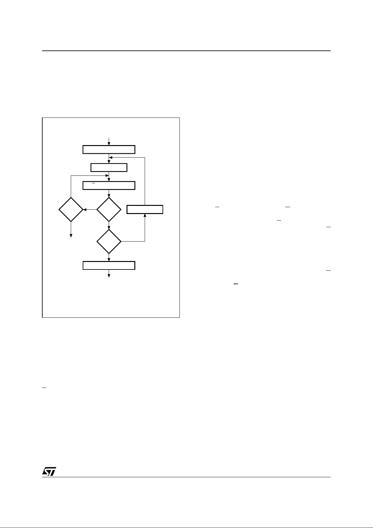
Figure 6. Programming Flowchart
VCC = 6.25V, VPP = 12.75V
SET MARGIN MODE
n = 0
E = 100µs Pulse
NO
NO
VERIFY
YES
Last
NO
Addr
YES
RESET MARGIN MODE
CHECK ALL BYTES
1st: VCC = 6V
2nd: VCC = 4.2V
++ Addr
AI00738B
YES
++n
= 25
FAIL
Programming
When delivered (and after each erasure for UV
EPROM), all bits of the M27C512 are in the '1'
state. Data is introduc ed by selectively programming '0's into the desired bit locations. Although
only '0's will be programmed, both '1's and '0's can
be present in the data word. The only way to
change a '0' to a '1' is by die exposure to ultraviolet
light (UV EPROM). The M27C512 is in the programming mode when V
is pulsed to VIL. The data to be programmed is
E
input is at 12.75V a nd
PP
applied to 8 bits in parallel to the data output pins.
The levels required for the address and data inputs are TTL. V
is specified to be 6.25V ±
CC
0.25V. The M27C512 can use P RESTO IIB Programming Algorithm that drastically reduces the
programming time (typi c ally les s tha n 6 secon d s).
Nevertheless to achieve c ompati bility with all p rogramming equipments, PRESTO Programming
Algorithm can be used as well.
PRESTO IIB Programming Algorithm
PRESTO IIB Programming Algorithm allows the
whole array to be programmed wi th a guarante ed
margin, in a typical time of 6.5 seconds. This can
be achieved with STMicroelectronics M27C512
due to several design innovations described in the
M27C512 datasheet to improve programming efficiency and to provide adequate margin for reliability. Before starting the programming the internal
MARGIN MODE circuit is set in order to guarantee
that each cell is programmed with enough margin.
Then a sequence of 100µs program pulses are applied to each byte until a correct veri fy occurs. No
overprogram pulses are applied since the verify in
MARGIN MODE provides the necessary margin.
Program Inhibit
Programming of multiple M27C512s in parallel
with different data is also easily accomplished. Except for E
, all like inputs including GVPP of the pa rallel M27C512 may be common . A TTL low level
pulse applied to a M27C512's E
input, with VPP at
12.75V, will program that M27C512. A high level E
input inhibits the other M27C512s from being programmed.
Program Verify
A verify (read) should be performed on the programmed bits to determine that they were correctly progra m me d. T he ve r i fy i s ac co mp l is he d w ith G
at VIL. Data should be verified with t
falling edge of E
.
ELQV
after the
Electronic Signature
The Electronic Signature (ES) mode allows the
reading out of a binary code from an EPROM that
will identify its manufacture r and type. This mode
is intended for use by programm ing equip ment to
automatica lly m atc h th e de vice t o be prog ra mmed
with its corresponding programming algorithm.
The ES mode is functional in the 25° C ± 5°C ambient temperature range that is required when programming the M27C512. To activate the ES
mode, the programming equipment must force
11.5V to 12.5V on address line A9 of the
M27C512. Two identifier bytes may then be sequenced from the device ou tputs by toggling address line A0 from V
lines must be he ld at V
ture mode. Byte 0 (A0 = V
ufacturer code and byte 1 (A0 = V
to VIH. All other address
IL
during Electronic Signa-
IL
) represents the man-
IL
) the device
IH
identifier code. For the STMicroelectronics
M27C512, these two identif ier bytes are given in
Table 3. and can be read-out on outputs Q7 to Q0.
7/22

M27C512
ERASURE OPERATION (APPLIES FOR UV EPROM)
The erasure characteristics of the M27C512 is
such that erasure begins when the cells are ex posed to light with wavelengt hs shorter than approximately 4000 Å. It should be noted that
sunlight and some type of fluorescent lamps have
wavelengths in the 3000-4000 Å range.
Research shows that constant ex posure to room
level fluorescent lighting could erase a typical
M27C512 in about 3 years, while it would take approximately 1 week to cause erasure when exposed to direct sunlight. If the M27C5 12 is to be
exposed to these typ es of lighting conditions for
extended periods of time, it is suggested that
opaque labels be put over the M27C512 window to
prevent unintentional e rasu re. The r ecomm ended
erasure procedure for the M27C512 is exposure to
short wave ultraviolet light whi ch has wavelength
2537 Å. The integrated dose ( i.e. UV intensity x
exposure time) for erasur e should be a minimum
of 15 W-sec/cm
age is approximately 15 to 20 minutes using an ultraviolet lamp with 12000 µW/cm
The M27C512 should be placed within 2.5 cm (1
inch) of the lamp tu bes during the erasur e. Some
lamps have a filter on th eir tub es whi ch shoul d be
removed before erasure.
2
. The erasure time with this dos-
2
power rating.
8/22

M27C512
MAXIMUM RATING
Stressing the devi ce outside the ratings li sted in
Table 4. may cause permanent damage to the de-
vice. These are stress ratings only, and oper ation
of the device at these, or any other conditions outside those indicated in the Oper ating sections of
Table 4. Absolute Maximum Ratings
Symbol Parameter Value Unit
T
A
T
BIAS
T
STG
T
LEAD
(2)
V
IO
V
CC
(2)
V
A9
V
PP
Note: 1. Compliant with the JEDEC Std J-STD-020B (for small body, Sn-Pb or Pb assermbly), the ST ECOPACK® 7191395 specification,
and the European directive on Restr i ctions on Hazardous Substances (RoHS) 2002/95/EU.
2. Minimum DC voltage on Input or Output is –0.5V with possible undershoot to –2.0V for a period less than 20ns. Maximum DC
voltage on Output is V
3. Depends on range.
Ambient Operatin g Temperature
Temperature Under Bias –50 to 125 °C
Storage Temperature –65 to 150 °C
Lead Temperature during Soldering (note 1) °C
Input or Output Voltage (except A9) –2 to 7 V
Supply Voltage –2 to 7 V
A9 Voltage –2 to 13.5 V
Program Supply Voltage –2 to 14 V
+0.5V with possible overshoot to VCC +2V for a period less than 20ns.
CC
(3)
this specificatio n, is not implied. Exposure to Absolute Maximum Rating conditions for extended
periods may affect de vice rel iability. Refer also to
the STMicroelectroni cs SURE Program and othe r
relevant quality documents.
–40 to 125 °C
9/22

M27C512
DC AND AC PARAMETERS
This section summ arizes the operati ng and measurement conditions , and the D C an d AC charac teristics of the device. The parameters in th e DC
and AC Characteristic tables that follow are derived from tests performed under the Measure-
Table 5. AC Measurement Conditions
Input Rise and Fall Times ≤ 10ns ≤ 20ns
Input Pulse Voltages 0 to 3V 0.4V to 2.4V
Input and Output Timing Ref. Voltages 1.5V 0.8V and 2V
Figure 7. Testing Input Output Waveform Figure 8. AC Testing Load Circuit
High Speed
3V
1.5V
0V
ment Conditions summarized in the relevant
tables. Designers sho uld c heck tha t th e operating
conditions in thei r circui t match the measur ement
conditions when relying on the quoted parameters.
High Speed Standard
1.3V
1N914
Ω
3.3k
Standard
2.4V
0.4V
Table 6. Capacitance
Symbol
C
IN
C
OUT
Note: 1. TA = 25°C, f = 1MHz
2. Sampled only, not 100% tested.
Input Capacitance
Output Capacitance
DEVICE
UNDER
TEST
2.0V
0.8V
AI01822
CL = 30pF for High Speed
CL = 100pF for Standard
CL includes JIG capacitance
Parameter Test Condition
V
= 0V
IN
V
= 0V
OUT
(1,2)
OUT
CL
AI01823B
Min Max Unit
6pF
12 pF
10/22

Table 7. Read Mode DC Characteristics
Symbol
Parameter Test Condition
(1)
M27C512
Min Max Unit
I
I
I
CC
I
CC1
I
CC2
I
V
V
IH
V
V
Note: 1. VCC must be applied simultaneously with or before VPP and removed simultaneously or aft er VPP.
Input Leakage Current
LI
Output Leakage Current
LO
Supply Current
I
OUT
0V ≤ V
0V ≤ V
E
Supply Current (Standby) TTL
Supply Current (Standby) CMOS
Program Current
PP
Input Low Voltage –0.3 0.8 V
IL
(2)
Input High Voltage 2
Output Low Voltage
OL
E
Output High Voltage TTL
OH
Output High Voltage CMOS
2. Maximum DC voltage on Output is V
CC
+0.5V.
≤ V
IN
CC
≤ V
OUT
CC
= VIL, G = VIL,
= 0mA, f = 5MHz
E
= V
IH
> VCC – 0.2V
V
= V
PP
CC
I
= 2.1mA
OL
I
= –1mA
OH
= –100µA VCC – 0.7V
I
OH
3.6 V
Table 8. Read Mode AC Characteristics
M27C512
Symbol Alt Parameter
t
AVQVtACC
t
ELQV
t
GLQVtOE
(2)
t
EHQZ
(2)
t
GHQZ
t
AXQXtOH
Note: 1. VCC must be applied simultaneously with or before VPP and removed simultaneously or aft er VPP.
2. Sampled only, not 100% tested.
3. Speed obtained with High Speed AC measurement conditions .
Address Valid to
Output Valid
Chip Enable Low to
t
CE
Output Valid
Output Enable Low
to Output Valid
Chip Enable High
t
DF
to Output Hi-Z
Output Enable
t
DF
High to Output Hi-Z
Address Transition
to Output Transition
Test Condition
= VIL, G = V
E
= V
G
= V
E
= V
G
= V
E
= VIL, G = V
E
(1)
IL
IL
IL
IL
IL
IL
-45
(3)
-60 -70 -80
MinMaxMinMaxMinMaxMinMax
45 60 70 80 ns
45 60 70 80 ns
25 30 35 40 ns
025025030030ns
025025030030ns
0000ns
±10 µA
±10 µA
30 mA
1mA
100 µA
10 µA
V
CC
+ 1
V
0.4 V
V
Unit
11/22

M27C512
Table 9. Read Mode AC Characteristics
M27C512
Symbol Alt Parameter
Test Condition
(1)
-90
MinMaxMinMaxMinMaxMinMax
t
AVQVtACC
t
ELQV
t
GLQVtOE
(2)
t
EHQZ
(2)
t
GHQZ
t
AXQXtOH
Note: 1. VCC must be applied simultaneously with or before VPP and removed simultaneously or aft er VPP.
2. Sampled only, not 100% tested.
Address Valid to
Output Valid
Chip Enable Low to
t
CE
Output Valid
Output Enable Low
to Output Valid
Chip Enable High
t
DF
to Output Hi-Z
Output Enable
t
DF
High to Output Hi-Z
Address Transition
to Output Transition
= VIL, G = V
E
= V
G
= V
E
= V
G
= V
E
= VIL, G = V
E
IL
IL
IL
IL
IL
IL
90 100 120 150 ns
90 100 120 150 ns
40 40 50 60 ns
030030040050ns
030030040050ns
0000ns
Figure 9. Read Mode AC Waveforms
-10 -12 -15/-20/-25
Unit
A0-A15
E
G
Q0-Q7
tAVQV
tELQV
VALID
tGLQV
VALID
tAXQX
tEHQZ
tGHQZ
Hi-Z
AI00735B
12/22

Table 10. Programming Mode DC Characteristics
Symbol
I
LI
I
CC
I
PP
V
IL
V
IH
V
OL
V
OH
V
ID
Note: 1. TA = 25 °C; VCC = 6.25V ± 0.25V; VPP = 12.75V ± 0.25V
2. V
Input Leakage Current
Supply Current 50 mA
Program Current
Input Low Voltage –0.3 0.8 V
Input High Voltage 2
Output Low Voltage
Output High Voltage TTL
A9 Voltage 11.5 12.5 V
must be applied simultaneously with or before VPP and removed simultaneously or aft er VPP.
CC
Parameter Test Condition
V
≤ VIN ≤ V
IL
E
= V
I
= 2.1mA
OL
I
= –1mA
OH
M27C512
(1,2)
IH
IL
Min Max Unit
±10 µA
50 mA
V
CC
+ 0.5
V
0.4 V
3.6 V
13/22

M27C512
Table 11. Margin Mode AC Characteristics
Symbol Alt Parameter
t
A9HVPH
t
VPHEL
t
A10HEH
t
A10LEH
t
EXA10X
t
EXVPX
t
VPXA9X
Note: 1. TA = 25 °C; VCC = 6.25V ± 0.25V; VPP = 12.75V ± 0.25V
2. V
Figure 10. Margin Mode AC Waveforms
t
t
t
AS10VA10
t
AS10VA10
t
AH10
t
t
must be applied simultaneously with or before VPP and removed simultaneously or aft er V
CC
V
CC
A8
VA9 High to VPP High
AS9
VPP High to Chip Enable Low
VPS
High to Chip Enable High (Set)
Low to Chip Enable High (Reset)
Chip Enable Transition to V
Chip Enable Transition to VPP Transition
VPH
VPP Transition to VA9 Transition
AH9
A10
Transition
Test Condition
(1,2)
Min Max Unit
2µs
2µs
1µs
1µs
1µs
2µs
2µs
PP.
A9
GV
PP
E
A10 Set
A10 Reset
Note: A8 High level = 5V; A9 High level = 12V.
tA9HVPH tVPXA9X
tVPHEL
tEXVPX
tA10HEH
tA10LEH
tEXA10X
AI00736B
14/22

Table 12. Programming Mode AC Characteristics
Symbol Alt
t
AVEL
t
QVEL
t
VCHEL
t
VPHEL
t
VPLVPH
t
ELEH
t
EHQX
t
EHVPX
t
VPLEL
t
ELQV
(3)
t
EHQZ
t
EHAX
Note: 1. TA = 25 °C; VCC = 6.25V ± 0.25V; VPP = 12.75V ± 0.25V
2. V
CC
3. Sampled only, not 100% tested.
t
Address Valid to Chip Enable Low 2 µs
AS
t
Input Valid to Chip Enable Low 2 µs
DS
t
t
t
t
t
t
OEH
t
must be applied simultaneously with or before VPP and removed simultaneously or aft er VPP.
VCC High to Chip Enable Low
VCS
VPP High to Chip Enable Low
OES
VPP Rise Time
PRT
Chip Enable Program Pulse Width (Initial) 95 105 µs
PW
Chip Enable High to Input Transition 2 µs
DH
Chip Enable High to VPP Transition
t
VPP Low to Chip Enable Low
VR
t
Chip Enable Low to Output Valid 1 µs
DV
Chip Enable High to Output Hi-Z 0 130 ns
DFP
t
Chip Enable High to Address Transition 0 ns
AH
Parameter Test Condition
(1,2)
M27C512
Min Max Unit
2µs
2µs
50 ns
2µs
2µs
Figure 11. Programming and Verify Modes AC Waveforms
A0-A15
Q0-Q7
V
CC
GV
PP
E
tAVEL
DATA IN
tQVEL
tVCHEL
tVPHEL
tELEH
PROGRAM
VALID
tEHQX
tEHVPX
tVPLEL
tEHAX
DATA OUT
tEHQZ
tELQV
VERIFY
AI00737
15/22

M27C512
PACKAGE MECHANICAL
Figure 12. FDIP28W - 28 pin Ceramic Frit-seal DIP, with window, Package Outline
A2
B1 B
A3
A1AL
e
α
C
eA
D2
eB
D
S
N
∅
1
Note: Drawing is not to scale.
E1 E
FDIPW-a
Table 13. FDIP28W - 28 pin Ceramic Frit-seal DIP, with window, Package Mechanical Data
Symbol
A 5.72 0.225
A1 0.51 1.40 0.020 0.055
A2 3.91 4.57 0.154 0.180
A3 3.89 4.50 0.153 0.177
B 0.41 0.56 0.016 0.022
B1 1.45 – – 0.057 – –
C 0.23 0.30 0.009 0.012
D 36.50 37.34 1.437 1.470
D233.02– –1.300– –
E 15.24 – – 0.600 – –
E1 13.06 13.36 0.514 0.526
e 2.54 – – 0.100 – –
eA 14.99 – – 0.590 – –
eB 16.18 18.03 0.637 0.710
L 3.18 4.10 0.125 0.161
S 1.52 2.49 0.060 0.098
∅ 7.11 – – 0.280 – –
α 4° 11° 4° 11°
N28 28
Typ Min Max Typ Min Max
millimeters inches
16/22

Figure 13. PDIP28 - 28 pin Plastic DIP, 600 mils width, Package Outline
A2
M27C512
A1AL
B1 B e1
D2
α
C
eA
eB
D
S
N
E1 E
1
Note: Drawing is not to scale.
PDIP
Table 14. PDIP28 - 28 pin Plastic DIP, 600 mils width, Package Mechanical Data
Symbol
Typ Min Max Typ Min Max
A 4.445 0.1750
A1 0.630 0.0248
A2 3.810 3.050 4.570 0.1500 0.1201 0.1799
B 0.450 0.0177
B1 1.270 0.0500
C 0.230 0.310 0.0091 0.0122
D 36.830 36.580 37.080 1.4500 1.4402 1.4598
D2 33.020 – – 1.3000 – –
E 15.240 0.6000
E1 13.720 12.700 14.480 0.5402 0.5000 0.5701
e1 2.540 – – 0.1000 – –
eA 15.000 14.800 15.200 0.5906 0.5827 0.5984
eB 15.200 16.680 0.5984 0.6567
L 3.300 0.1299
S 1.78 2.08 0.070 0.082
α 0° 10° 0° 10°
N28 28
millimeters inches
17/22

M27C512
Figure 14. PLCC32 - 32 lead Plastic Leaded Chip Carrier, Package Outline
D
D1
1 N
A1
A2
B1
E2
E3
E1 E
F
0.51 (.020)
B
E2
e
1.14 (.045)
D3
R
A
CP
D2 D2
PLCC-A
Note: Drawing is not to scale.
Table 15. PLCC32 - 32 lead Plastic Leaded Chip Carrier, Package Mechanical Data
Symbol
A 3.18 3.56 0.125 0.140
A1 1.53 2.41 0.060 0.095
A2 0.38 – 0.015 –
B 0.33 0.53 0.013 0.021
B1 0.66 0.81 0.026 0.032
CP 0.10 0.004
D 12.32 12.57 0.485 0.495
D1 11.35 11.51 0.447 0.453
D2 4.78 5.66 0.188 0.223
D3 7.62 – – 0.300 – –
E 14.86 15.11 0.585 0.595
E1 13.89 14.05 0.547 0.553
E2 6.05 6.93 0.238 0.273
E310.16– –0.400– –
e 1.27 – – 0.050 – –
F 0.00 0.13 0.000 0.005
R 0.89 – – 0.035 – –
N32 32
Typ Min Max Typ Min Max
millimeters inches
18/22

Figure 15. TSOP28 - 28 lead Plastic Thin Small Outline, 8 x 13.4 mm, Package Outline
A2
M27C512
1
N
e
E
B
N/2
D1
D
DIE
A
CP
C
TSOP-a
Note: Drawing is not to scale
LA1 α
Table 16. TSOP28 - 28 lead Plastic Thin Small Outline, 8 x 13.4 mm, Package Mechanical Data
millimeters inches
Symbol Typ Min Max Typ Min Max
A 1.250 0.0492
A1 0.200 0.0079
A2 0.950 1.150 0.0374 0.0453
B 0.170 0.270 0.0067 0.0106
C 0.100 0.210 0.0039 0.0083
CP 0.100 0.0039
D 13.200 13.600 0.5197 0.5354
D1 11.700 11.900 0.4606 0.4685
e 0.550 – – 0.0217 – –
E 7.900 8.100 0.3110 0.3189
L 0.500 0.700 0.0197 0.0276
α 0° 5° 0° 5°
N28 28
19/22

M27C512
PART NUMBERING
Table 17. Ordering Information Scheme
Example: M27C512 -70 X C 1 TR
Device Type
M27
Supply Voltage
C = 5V
Device Function
512 = 512 Kbit (64Kb x8)
Speed
(1)
= 45 ns
-45
-60 = 60 ns
-70 = 70 ns
-80 = 80 ns
-90 = 90 ns
-10 = 100 ns
-12 = 120 ns
-15 = 150 ns
-20 = 200 ns
-25 = 250 ns
VCC Tolerance
blank = ± 10%
X = ± 5%
Package
F = FDIP28W
B = PDIP28
C = PLCC32
N = TSOP28: 8 x 13.4 mm
Temperature Range
1 = 0 to 70 °C
3 = –40 to 125 °C
6 = –40 to 85 °C
Options
Blank = Standard Packing
TR = Tape and Reel Packing
E = Lead-free and RoHS Package, Standard Packing
F = Lead-free and RoHS Package, T ape and Reel Packing
Note: 1. High Speed, see AC Characteristics section for further information.
For a list of available options (speed, package,
etc.) or for further information on any aspect of this
device, please conta ct yo ur nearest ST Sal es Office.
20/22

REVISION HISTORY
Table 18. Revision History
Date Version Revision Details
November 1998 1.0 First Issue
25-Sep-2000 1.1 AN620 Reference removed
02-Apr-2001 1.2 FDIP28W mechanical dimensions changed (Table 13.)
29-Aug-2002 1.3
08-Nov-2004 2.0
Package mechanical data clarified for PDIP28 (Table 14.),
PLCC32 (Table 15., Figure 14.) and TSOP28 (Table 16., Figure 15.)
Details of ECOPACK lead-free package options added.
Additional Burn-in option removed
M27C512
21/22

M27C512
Information furnished is be lieved to be a ccur ate and reli able. Howe ver, STMicroele ctronic s assu mes no r esponsib ilit y for th e consequences
of use of such information nor for any infrin gement of patent s or other rights of third parties which ma y result from it s use. No license is granted
by implication or otherwi se under any patent or patent rights of STMicroelectronics. Specifications mentioned in this publication are subject
to change without not ice. This pub licat ion su persed es and repl aces all in format ion previou sly su pplie d. STMicroele c tronic s prod ucts ar e no t
authorized for use as critical compone nts in life support devices or systems witho ut express written approval of STMicroelectronics.
The ST logo is a registered trademark of STMicroelectronics.
All other names are the property of their respective owners
© 2004 STMicroelectronics - All rights reserved
Australia - Belgium - Brazil - Canada - China - Czech Republic - Finland - France - Germany - Hong Kong - India - Israel - Italy - Japan -
Malaysia - Malta - Morocco - Singapore - Spain - Sweden - Switzerland - United Kingdom - United States of America
STMicroelectronics group of companies
www.st.com
22/22
 Loading...