

8 Mbit, Low Voltage, Serial Flash Memory
FEAT URES SUMMARY
■ 8 Mbit of Flash M emor y
■ Page Program (up to 256 Bytes) in 1.4ms
(typical)
■ Sector Erase (512 Kbit) in 1s (typical)
■ Bulk Erase (8 Mbit) in 10s (typical)
■ 2.7 to 3.6V Single Supply Voltage
■ SPI Bus Compatible Serial Interface
■ 40MHz Clock Rate (maximum)
■ Deep Power-down Mode 1µA (typical)
■ Electronic Signature (13h)
M25P80
With 40MHz SPI Bus Interface
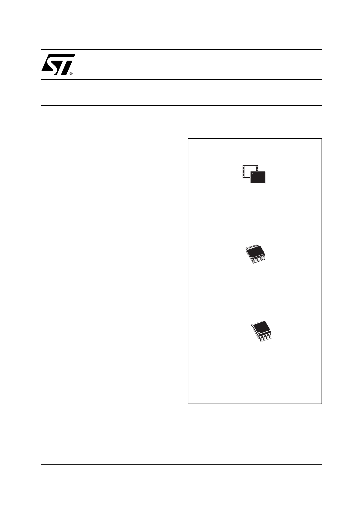
Figure 1. Packages
VDFPN8 (MP)
(MLP8)
SO16 (MF)
300 mil width
8
1
SO8 (MW)
200 mil width
1/41August 2004

M25P80
TABLE OF CONTENTS
FEATURES SUMMARY . . . . . . . . . . . . . . . . . . . . . . . . . . . . . . . . . . . . . . . . . . . . . . . . . . . . . . . . . . . . . 1
Figure 1. Packages. . . . . . . . . . . . . . . . . . . . . . . . . . . . . . . . . . . . . . . . . . . . . . . . . . . . . . . . . . . . . . 1
SUMMARY DESCRIPTION. . . . . . . . . . . . . . . . . . . . . . . . . . . . . . . . . . . . . . . . . . . . . . . . . . . . . . . . . . . 5
Figure 2. Logic Diagram . . . . . . . . . . . . . . . . . . . . . . . . . . . . . . . . . . . . . . . . . . . . . . . . . . . . . . . . . . 5
Table 1. Signal Names . . . . . . . . . . . . . . . . . . . . . . . . . . . . . . . . . . . . . . . . . . . . . . . . . . . . . . . . . . 5
Figure 3. VDFPN and SO8 Connections . . . . . . . . . . . . . . . . . . . . . . . . . . . . . . . . . . . . . . . . . . . . . 5
Figure 4. SO16 Connections. . . . . . . . . . . . . . . . . . . . . . . . . . . . . . . . . . . . . . . . . . . . . . . . . . . . . . . 5
SIGNAL DESCRIPTION . . . . . . . . . . . . . . . . . . . . . . . . . . . . . . . . . . . . . . . . . . . . . . . . . . . . . . . . . . . . . 6
Serial Data Output (Q). . . . . . . . . . . . . . . . . . . . . . . . . . . . . . . . . . . . . . . . . . . . . . . . . . . . . . . . . . . . 6
Serial Data Input (D) . . . . . . . . . . . . . . . . . . . . . . . . . . . . . . . . . . . . . . . . . . . . . . . . . . . . . . . . . . . . . 6
Serial Clock (C) . . . . . . . . . . . . . . . . . . . . . . . . . . . . . . . . . . . . . . . . . . . . . . . . . . . . . . . . . . . . . . . . . 6
Chip Select (S) . . . . . . . . . . . . . . . . . . . . . . . . . . . . . . . . . . . . . . . . . . . . . . . . . . . . . . . . . . . . . . . . . 6
Hold (HOLD) . . . . . . . . . . . . . . . . . . . . . . . . . . . . . . . . . . . . . . . . . . . . . . . . . . . . . . . . . . . . . . . . . . . 6
Write Protect (W). . . . . . . . . . . . . . . . . . . . . . . . . . . . . . . . . . . . . . . . . . . . . . . . . . . . . . . . . . . . . . . . 6
SPI MODES. . . . . . . . . . . . . . . . . . . . . . . . . . . . . . . . . . . . . . . . . . . . . . . . . . . . . . . . . . . . . . . . . . . . . . . 7
Figure 5. Bus Master and Memory Devices on the SPI Bus. . . . . . . . . . . . . . . . . . . . . . . . . . . . . . . 7
Figure 6. SPI Modes Supported . . . . . . . . . . . . . . . . . . . . . . . . . . . . . . . . . . . . . . . . . . . . . . . . . . . . 7
OPERATING FEATURES. . . . . . . . . . . . . . . . . . . . . . . . . . . . . . . . . . . . . . . . . . . . . . . . . . . . . . . . . . . . 8
Page Programming . . . . . . . . . . . . . . . . . . . . . . . . . . . . . . . . . . . . . . . . . . . . . . . . . . . . . . . . . . . . . 8
Sector Erase and Bulk Erase . . . . . . . . . . . . . . . . . . . . . . . . . . . . . . . . . . . . . . . . . . . . . . . . . . . . . 8
Polling During a Write, Program or Erase Cycle . . . . . . . . . . . . . . . . . . . . . . . . . . . . . . . . . . . . . 8
Active Power, Stand-by Power and Deep Power-Down Modes. . . . . . . . . . . . . . . . . . . . . . . . . . 8
Status Register . . . . . . . . . . . . . . . . . . . . . . . . . . . . . . . . . . . . . . . . . . . . . . . . . . . . . . . . . . . . . . . . 8
WIP bit. . . . . . . . . . . . . . . . . . . . . . . . . . . . . . . . . . . . . . . . . . . . . . . . . . . . . . . . . . . . . . . . . . . . . . . . 8
WEL bit . . . . . . . . . . . . . . . . . . . . . . . . . . . . . . . . . . . . . . . . . . . . . . . . . . . . . . . . . . . . . . . . . . . . . . . 8
BP2, BP1, BP0 bits . . . . . . . . . . . . . . . . . . . . . . . . . . . . . . . . . . . . . . . . . . . . . . . . . . . . . . . . . . . . . . 8
SRWD bit. . . . . . . . . . . . . . . . . . . . . . . . . . . . . . . . . . . . . . . . . . . . . . . . . . . . . . . . . . . . . . . . . . . . . . 8
Protection Modes . . . . . . . . . . . . . . . . . . . . . . . . . . . . . . . . . . . . . . . . . . . . . . . . . . . . . . . . . . . . . . 9
Table 2. Protected Area Sizes. . . . . . . . . . . . . . . . . . . . . . . . . . . . . . . . . . . . . . . . . . . . . . . . . . . . . 9
Hold Condition. . . . . . . . . . . . . . . . . . . . . . . . . . . . . . . . . . . . . . . . . . . . . . . . . . . . . . . . . . . . . . . . 10
Figure 7. Hold Condition Activation. . . . . . . . . . . . . . . . . . . . . . . . . . . . . . . . . . . . . . . . . . . . . . . . . 10
MEMORY ORGANIZATION . . . . . . . . . . . . . . . . . . . . . . . . . . . . . . . . . . . . . . . . . . . . . . . . . . . . . . . . . 11
Table 3. Memory Organization . . . . . . . . . . . . . . . . . . . . . . . . . . . . . . . . . . . . . . . . . . . . . . . . . . .11
Figure 8. Block Diagram . . . . . . . . . . . . . . . . . . . . . . . . . . . . . . . . . . . . . . . . . . . . . . . . . . . . . . . . . 12
INSTRUCTIONS . . . . . . . . . . . . . . . . . . . . . . . . . . . . . . . . . . . . . . . . . . . . . . . . . . . . . . . . . . . . . . . . . . 13
Table 4. Instruction Set . . . . . . . . . . . . . . . . . . . . . . . . . . . . . . . . . . . . . . . . . . . . . . . . . . . . . . . . . 13
Write Enable (WREN) . . . . . . . . . . . . . . . . . . . . . . . . . . . . . . . . . . . . . . . . . . . . . . . . . . . . . . . . . . 14
2/41

M25P80
Figure 9. Write Enable (WREN) Instruction Sequence. . . . . . . . . . . . . . . . . . . . . . . . . . . . . . . . . . 14
Write Disable (WRDI). . . . . . . . . . . . . . . . . . . . . . . . . . . . . . . . . . . . . . . . . . . . . . . . . . . . . . . . . . . 14
Figure 10.Write Disable (WRDI) Instruction Sequence . . . . . . . . . . . . . . . . . . . . . . . . . . . . . . . . . . 14
Read Status Register (RDSR). . . . . . . . . . . . . . . . . . . . . . . . . . . . . . . . . . . . . . . . . . . . . . . . . . . . 15
Table 5. Status Register Format . . . . . . . . . . . . . . . . . . . . . . . . . . . . . . . . . . . . . . . . . . . . . . . . . . 1 5
WIP bit. . . . . . . . . . . . . . . . . . . . . . . . . . . . . . . . . . . . . . . . . . . . . . . . . . . . . . . . . . . . . . . . . . . . . . . 15
WEL bit . . . . . . . . . . . . . . . . . . . . . . . . . . . . . . . . . . . . . . . . . . . . . . . . . . . . . . . . . . . . . . . . . . . . . . 15
BP2, BP1, BP0 bits . . . . . . . . . . . . . . . . . . . . . . . . . . . . . . . . . . . . . . . . . . . . . . . . . . . . . . . . . . . . . 15
SRWD bit. . . . . . . . . . . . . . . . . . . . . . . . . . . . . . . . . . . . . . . . . . . . . . . . . . . . . . . . . . . . . . . . . . . . . 15
Figure 11.Read Status Register (RDSR) Instruction Sequence and Data-Out Sequence . . . . . . . 15
Write Status Register (WRSR) . . . . . . . . . . . . . . . . . . . . . . . . . . . . . . . . . . . . . . . . . . . . . . . . . . . 16
Figure 12.Write Status Register (WRSR) Instruction Sequence . . . . . . . . . . . . . . . . . . . . . . . . . . . 16
Table 6. P rote ction Modes. . . . . . . . . . . . . . . . . . . . . . . . . . . . . . . . . . . . . . . . . . . . . . . . . . . . . . . 1 7
Read Data Bytes (READ). . . . . . . . . . . . . . . . . . . . . . . . . . . . . . . . . . . . . . . . . . . . . . . . . . . . . . . . 18
Figure 13.Read Data Bytes (READ) Instruction Sequence and Data-Out Sequence . . . . . . . . . . . 18
Read Data Bytes at Higher Speed (FAST_READ). . . . . . . . . . . . . . . . . . . . . . . . . . . . . . . . . . . . 19
Figure 14.Read Data Bytes at Higher Speed (FAST_READ) Instruction Sequence and Data-Out Sequence 19
Page Program (PP) . . . . . . . . . . . . . . . . . . . . . . . . . . . . . . . . . . . . . . . . . . . . . . . . . . . . . . . . . . . . 20
Figure 15.Page Program (PP) Instruction Sequence . . . . . . . . . . . . . . . . . . . . . . . . . . . . . . . . . . . 20
Sector Erase (SE) . . . . . . . . . . . . . . . . . . . . . . . . . . . . . . . . . . . . . . . . . . . . . . . . . . . . . . . . . . . . . 21
Figure 16.Sector Erase (SE) Instruction Sequence. . . . . . . . . . . . . . . . . . . . . . . . . . . . . . . . . . . . . 21
Bulk Erase (BE) . . . . . . . . . . . . . . . . . . . . . . . . . . . . . . . . . . . . . . . . . . . . . . . . . . . . . . . . . . . . . . . 22
Figure 17.Bulk Erase (BE) Instruction Sequence . . . . . . . . . . . . . . . . . . . . . . . . . . . . . . . . . . . . . . 22
Deep Power-down (DP). . . . . . . . . . . . . . . . . . . . . . . . . . . . . . . . . . . . . . . . . . . . . . . . . . . . . . . . . 23
Figure 18.Deep Power-down (DP) Instruction Sequence . . . . . . . . . . . . . . . . . . . . . . . . . . . . . . . . 23
Rele ase fr om Deep Power - down an d R e a d Electronic Signature ( R ES) . . . . . . . . . . . . . . . . . 24
Figure 19.Release from Deep Power-down and Read Electronic Signature (RES) Instruction Sequence and Data-Out Sequence24
Figure 20.Release from Deep Power-down (RES) Instruction Sequence. . . . . . . . . . . . . . . . . . . . 25
POWER-UP AND POWER-DOWN . . . . . . . . . . . . . . . . . . . . . . . . . . . . . . . . . . . . . . . . . . . . . . . . . . . . 26
Figure 21.Power-up Timing. . . . . . . . . . . . . . . . . . . . . . . . . . . . . . . . . . . . . . . . . . . . . . . . . . . . . . . 27
Table 7. Power-Up Timing and VWI Threshold. . . . . . . . . . . . . . . . . . . . . . . . . . . . . . . . . . . . . . .27
INITIAL DELIVERY STATE. . . . . . . . . . . . . . . . . . . . . . . . . . . . . . . . . . . . . . . . . . . . . . . . . . . . . . . . . . 27
MAXIMUM RATING. . . . . . . . . . . . . . . . . . . . . . . . . . . . . . . . . . . . . . . . . . . . . . . . . . . . . . . . . . . . . . . . 28
Table 8. Absolute Maximum Ratings. . . . . . . . . . . . . . . . . . . . . . . . . . . . . . . . . . . . . . . . . . . . . . . 28
DC AND AC PARAMETERS. . . . . . . . . . . . . . . . . . . . . . . . . . . . . . . . . . . . . . . . . . . . . . . . . . . . . . . . . 29
Table 9. Operating Conditions. . . . . . . . . . . . . . . . . . . . . . . . . . . . . . . . . . . . . . . . . . . . . . . . . . . . 29
Table 10. Data Retention and Endurance. . . . . . . . . . . . . . . . . . . . . . . . . . . . . . . . . . . . . . . . . . . . 29
Table 11.Capacitance. . . . . . . . . . . . . . . . . . . . . . . . . . . . . . . . . . . . . . . . . . . . . . . . . . . . . . . . . . . 2 9
Table 12. DC Characteristics (Device Grade 6) . . . . . . . . . . . . . . . . . . . . . . . . . . . . . . . . . . . . . . .30
Table 13. DC Characteristics (Device Grade 3) . . . . . . . . . . . . . . . . . . . . . . . . . . . . . . . . . . . . . . .30
3/41

M25P80
Table 14. Instruction Times (Device Grade 6). . . . . . . . . . . . . . . . . . . . . . . . . . . . . . . . . . . . . . . . . 31
Table 15. Instruction Times (Device Grade 3). . . . . . . . . . . . . . . . . . . . . . . . . . . . . . . . . . . . . . . . . 31
Table 16. AC Measurement Condition s. . . . . . . . . . . . . . . . . . . . . . . . . . . . . . . . . . . . . . . . . . . . . . 31
Figure 22.AC Measurement I/O Waveform. . . . . . . . . . . . . . . . . . . . . . . . . . . . . . . . . . . . . . . . . . . 31
Table 17. AC Characteristics (25MHz Operation, Device Grade 6 or 3) . . . . . . . . . . . . . . . . . . . . . 32
Table 18. AC Characteristics (40MHz Operation, Device Grade 6) . . . . . . . . . . . . . . . . . . . . . . . . 33
Figure 23.Serial Input Timing . . . . . . . . . . . . . . . . . . . . . . . . . . . . . . . . . . . . . . . . . . . . . . . . . . . . . 34
Figure 24.Write Protect Setup and Hold Timing during WRSR when SRWD=1 . . . . . . . . . . . . . . . 34
Figure 25.Hold Timing. . . . . . . . . . . . . . . . . . . . . . . . . . . . . . . . . . . . . . . . . . . . . . . . . . . . . . . . . . . 35
Figure 26.Output Timing . . . . . . . . . . . . . . . . . . . . . . . . . . . . . . . . . . . . . . . . . . . . . . . . . . . . . . . . . 35
PACKAGE MECHANICAL . . . . . . . . . . . . . . . . . . . . . . . . . . . . . . . . . . . . . . . . . . . . . . . . . . . . . . . . . . 36
Figure 27.VDFPN8 (MLP8) 8-lead Very thin Dual Flat Package No lead, Package Outline. . . . . . 36
Table 19. VDFPN8 (MLP8) 8-lead Very thin Dual Flat Package No lead, Package Mechanical Data
36
Figure 28.SO16 wide – 16-lead Plastic Small Outline, 300 mils body width, Package Outline. . . . 37
Table 20. SO16 wide – 16-lead Plastic Small Outline, 300 mils body width, Mechanical Data. . . . 37
Figure 29.SO8 wide – 8 lead Plastic Small Outline, 200 mils body width, Package Outline. . . . . . 38
Table 21. SO8 wide – 8 lead Plastic Small Outline, 200 mils body width, Package Mechan ical Data
38
PART NUMBERING . . . . . . . . . . . . . . . . . . . . . . . . . . . . . . . . . . . . . . . . . . . . . . . . . . . . . . . . . . . . . . . 39
Table 22.Ordering Information Scheme . . . . . . . . . . . . . . . . . . . . . . . . . . . . . . . . . . . . . . . . . . . . . 39
REVISION HISTORY. . . . . . . . . . . . . . . . . . . . . . . . . . . . . . . . . . . . . . . . . . . . . . . . . . . . . . . . . . . . . . . 40
Table 23. Document Revision History. . . . . . . . . . . . . . . . . . . . . . . . . . . . . . . . . . . . . . . . . . . . . . . 40
4/41
SUMMARY DESCRIPT ION
The M25P80 is a 8 Mbit (1M x 8) Serial Flash
Memory, with advanced write protection mechanisms, accessed by a high spee d SPI-compatible
bus.
The memory can be programmed 1 to 256 bytes at
a time, using the Page Program instruction.
The memory is organized as 16 sectors, each containing 256 pages. Each page is 256 byt es wide.
Thus, the whole memory can be viewed as consisting of 4096 pages, or 1,048,576 bytes.
The whole memory can b e erased using t he Bulk
Erase instruction, or a sector at a time, using the
Sector Erase instruction.
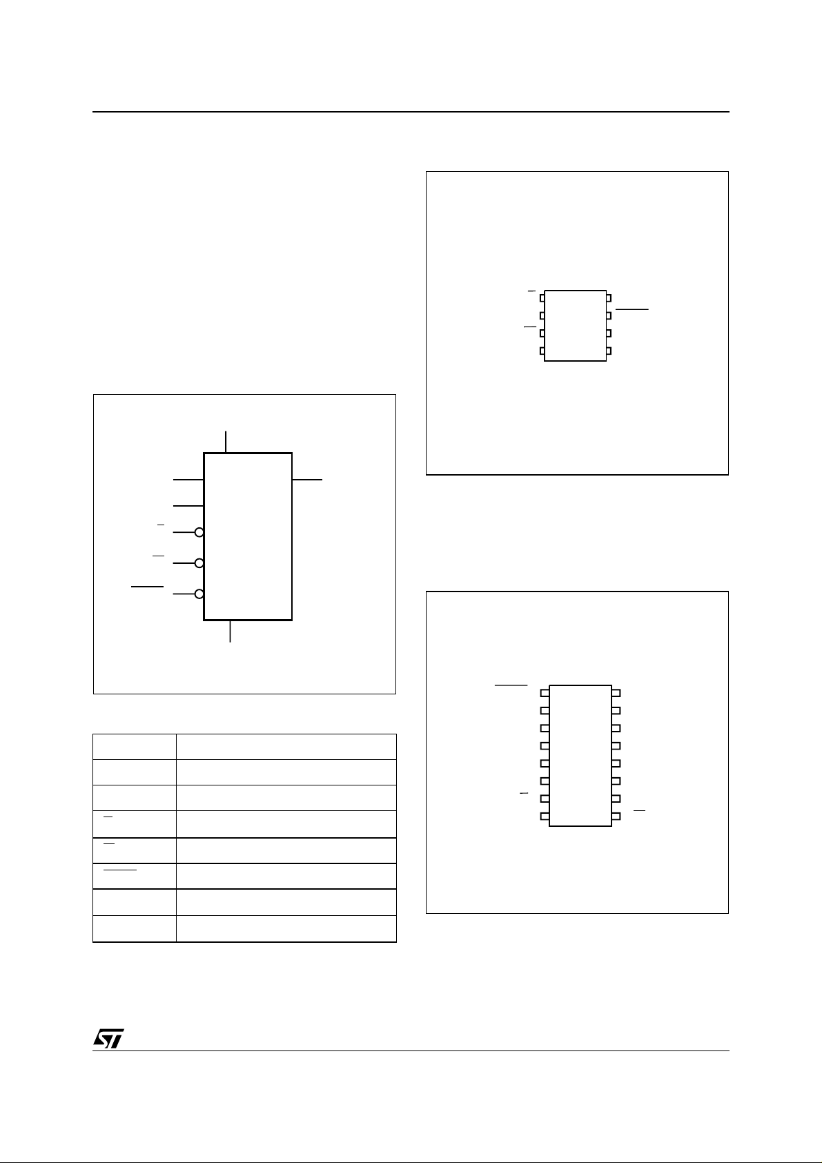
Figure 2. Logic Diagram
V
CC
Figure 3. VD FP N a nd SO8 C onnections
M25P80
SV
1
2
W
3
4
SS
8
7
6
5
AI04965B
CC
HOLDQ
C
DV
M25P80
D
C
S
M25P80
W
HOLD
V
SS
Table 1. Signal Names
C Serial Clock
D Serial Data Input
Q Serial Data Output
S
Write Protect
W
HOLD
Hold
Chip Select
Q
Note: 1. There is an expose d die paddle on the unde rside of th e
MLP8 package. This is pulled, internally, to V
must not be allowed to be connected to any other voltage
or signal line on the PCB.
2. See PACKAGE MECHANICAL section for package dimensions, and how to identify pi n-1.
SS
, and
Figure 4. SO16 Connec tions
AI04964
HOLD
V
CC
DU
DU
DU
M25P80
C
16
1
2
3
4
5
6
S
7
8
AI09712
15
14
13
12
11
10
D
DUDU
DU
DU
DU
V
SS
WQ
9
V
CC
V
SS
Supply Voltage
Ground
Note: 1. DU = Don’t Us e
2. See PACKAGE MECHANICAL section for package dimensions, and how to identify pi n-1.
5/41

M25P80
SIGNAL DESCRIPTION
Serial Data Output (Q). This output signal is
used to transfer data serially out of the device.
Data is shifted out on the falling edge of Serial
Clock (C).
Serial Data Input (D). This input signal is used to
transfer data serially into the device. It receives instructions, addresses, and the data to be programmed. Values are latched on the rising edge of
Serial Clock (C).
Serial Clock (C). This input signal provides the
timing of the serial interface. Instructions, addresses, or data present at Serial Data Input (D) are
latched on the rising edge of Serial Clock (C). Data
on Serial Data Output (Q) changes after the falling
edge of Serial Clock (C).
Chip Select (S
the device is des elected and Serial Data Ou tput
(Q) is at high impedance. Unless an internal Program, Erase or Write Status Register cycle is in
progress, the device w ill be in the S tandby mode
). When this input signal is High,
(this is not the Deep Power-down mode). Driving
Chip Selec t ( S
in the active power mode.
After Power-up, a falling edge on Chip Select (S
is required prior to the start of any instruction.
Hold (HOLD
pause any serial communications with the device
without deselecting the device.
During the Hold condition, the Serial Data Output
(Q) is high impedanc e, and Serial D ata Input (D)
and Serial Clock (C) are Don’t Care.
To start the Hold condition, the device must be selected, wit h Ch ip Select (S
Write Protect (W
put signal is to freeze the size of the area of memory that is protected against program or erase
instructions (as specified by the values in the BP2,
BP1 and BP0 bits of the Status Register).
) Low enables the device, placing it
). The Hold (HOLD) signal is used to
) driven Low.
). The main purpose of this in-
)
6/41
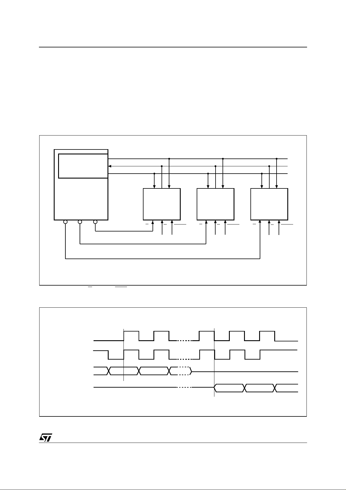
SPI MODES
These devices can be drive n by a microcont roller
with its SPI peripheral running in either of the two
following modes:
– CPOL=0, CPHA=0
– CPOL=1, CPHA=1
For these two modes, input data is latc hed in on
the rising edge of Serial Clock (C), and output data
Figure 5. Bus Master and Memory Devices on the SPI Bus
is avai lable from t he falling edge of S erial Clock
(C).
The difference between the two modes, as shown
in Figure 6., is the clock polarity when the bus
master is in Stand-by mode and not transferring
data:
– C remains at 0 for (CPOL=0, CPHA=0)
– C remains at 1 for (CPOL=1, CPHA=1)
M25P80
SPI Interface with
(CPOL, CPHA) =
(0, 0) or (1, 1)
Bus Master
(ST6, ST7, ST9,
ST10, Others)
CS3 CS2 CS1
Note: The Write Protect (W) and Hold (HOLD) signals sh oul d be driven, High or Low as appropriate.
SDO
SDI
SCK
CQD
SPI Memory
Device
S
CQD
SPI Memory
Device
HOLD
W
S
W
Figure 6. SPI Mo de s S upported
CPHA
CPOL
HOLD
CQD
SPI Memory
Device
S
W
AI03746D
HOLD
0
0
1
1
C
C
D
Q
MSB
MSB
AI01438B
7/41

M25P80
OPERATING FEAT URES
Page Prog ram m i ng
To program one data byte, two instructions are required: Write Enable (WREN), which is one by te,
and a Page Program (PP) sequence, which consists of four bytes plus data. This is followed by the
internal Program cycle (of duration t
To spread this overhead, the Page P rogram (PP)
instruction allows up to 256 bytes to be programmed at a time (changing bits from 1 to 0), provided that they lie in consecutive addresses on the
same page of memory.
Sector Erase and Bulk Erase
The Page Program (PP) instruction allows bits to
be reset from 1 to 0. Before this can be applied, the
bytes of memory need to hav e been erased to a ll
1s (FFh). This can be achieved either a sector at a
time, using the Sector Erase (SE) instruction, or
throughout the entire memory, using the Bulk
Erase (BE) instruction. This starts an internal
Erase cycle (of duration t
or tBE).
SE
The Erase instruction must be preceded by a Write
Enable (WREN) instruction.
Polling During a Write, Program or Erase Cycle
A further improvement in the time to Write Status
Register (WRSR), Program (PP) or Erase (SE or
BE) can be achieved by n ot waiting for the worst
case delay (t
, tPP, tSE, or tBE). The Write In
W
Progress (WIP) bit is provided in the Status Register so that the application program can monitor its
value, polling it to establish when the previous
Write cycle, Program cycle or Erase cycle is complete.
Active Power , Sta nd - by Power and Deep Power-Down Modes
When Chip Select (S
) is Low, the device is en-
abled, and in the Active Power mode.
When Chip Select (S
) is High, the device is disabled, but could remain in the Active Power mode
until all internal cycles have completed (Program,
PP
).
Erase, Write Status Register). The device then
goes in to the S tand-by Power m ode. The device
consumption drops to I
CC1
.
The Deep Power-down mode is entered when the
specific instruction (the Enter Deep Power-down
Mode (DP) instruction) is executed. The device
consumption drops further to I
. The device re-
CC2
mains in this mode until another specific instruction (the Release from Deep Power-down Mode
and Read Electro nic Signature (RE S) instruction)
is executed.
All other instructions are ignored while the device
is in the Deep Power-down mode. This can be
used as an extra software protection mecha nism,
when the device is not in active use, to protect the
device from inadvertent Write, Pr ogram or Erase
instructions.
Status Register
The Status Register contains a number of status
and control bits that can be read or set (as appropriate) by specific instructions.
WIP bit. The Write In Progress (WIP) bit indicates
whether the memory is busy with a Write Status
Register, Program or Erase cycle.
WEL bit. The Write Enable Latch (WEL) bit i ndicates the status of the internal Write Enable Latch.
BP2, BP1, BP0 bits. The Block Protect (BP2,
BP1, BP0) bits are non-volatile. They define the
size of the area to be software protected against
Program and Erase instructions.
SRWD bit. The Status Register Write Disable
(SRWD) bit is operated in conjunction with the
Write Protect (W
) signal. The Status Register
Write Disable (SRWD) bit an d Write Protect (W
signal allow the device to be put in the Hardware
Protected mode. In this mode, the non-volatile bits
of the Status Register (SRWD, BP2, BP1, BP0)
become read-only bits.
)
8/41
M25P80
Protectio n Modes
The environments where non-volatile memory devices are used can be very noisy. No SPI dev ice
can operate correctly in the presence of excessive
noise. To help combat this, the M25P80 boasts the
following data protection mechanisms:
■ Power-On Reset and an internal timer (t
PUW
can provide protection against inadvertant
changes while the power supply is outside the
operating specification.
■ Program, Erase and Write Status Register
instructions are checked that they consist of a
number of clock pulses that is a multiple of
eight, before they are accepted for execution.
■ All instructions that modify data must be
preceded by a Write Enable (WREN)
instruction to set the Write Enable Latch
(WEL) bit . This bit is returned to its reset state
by the following events:
– Power-up
– Write Disable (WRDI) instruction
)
– Write Status Register (WRSR) instruction
completion
– Page Program (PP) instruction completion
– Sector Erase (SE) instruction completion
– Bulk Erase (BE) instruction completion
■ The Block Prote ct (BP2, BP1, BP0 ) b its allow
part of the memory to be configured as readonly. This is the Software Protected Mode
(SPM).
■ The Write Protect (W) signal allows the Block
Protect (BP2, BP1, BP0) bits and Status
Register Write Disable (SRWD) bit to be
protected. This is the Hardware Protected
Mode (HPM).
■ In addition to the low power consumption
feature, the Deep Power-down mode offers
extra software protection from inadvertant
Write, Program and Erase instructions, as all
instructions are ignored except one particular
instruction (the Release from Deep Powerdown instruction).
completion
Table 2. Protected Area Sizes
Status Register
Content
BP2
Bit
BP1
Bit
0 0 0 none
0 0 1 Upper sixteenth (Sector 15) Lower fifteen-sixteenths (fifteen sectors: 0 to 14)
BP0
Bit
Protected Area Unprotected Area
Memory Content
All sectors
1
(sixteen sectors: 0 to 15)
0 1 0 Upper eighth (two sectors: 14 and 15) Lower seven-eighths (fourteen sectors: 0 to 13)
0 1 1 Upper quarter (four sectors: 12 to 15) Lower three-quarters (twelve sectors: 0 to 11)
1 0 0 Upper half (eight sectors: 8 to 15) Lower half (eight sectors: 0 to 7)
1 0 1 All sectors (sixteen sectors: 0 to 15) none
1 1 0 All sectors (sixteen sectors: 0 to 15) none
1 1 1 All sectors (sixteen sectors: 0 to 15) none
Note: 1. The device is ready to accept a Bulk Erase inst ruction if, and only if, all Block Protect (BP2, BP1, BP0) are 0.
9/41
M25P80
Hold Condition
The Hold (HOLD
) signal is used to pause any serial communications with the device without resetting the clocking sequence. Howev er, taking this
signal Low does not terminate any Write Status
Register, Program or Erase cycle that is currently
in progress.
To enter the Hold condition, the device must be
selecte d, with Chip Selec t (S
) Low.
The Hold condition starts on the falling edge of the
Hold (HOLD
) signal, provided that t his coincides
with Serial Clock (C) being Low (as shown i n Fig-
ure 7.).
The Hold condition ends on the rising edge of the
Hold (HOLD
) signal, provided that t his coincides
with Serial Clock (C) being Low.
If the falling edge does not coincide with Serial
Clock (C) being Low, the Hold condition starts after Serial Clock (C) next goes Low. Similarly, if the
Figure 7. Hold Condition Activation
C
rising edge does not coincide with Serial Clock (C)
being Low, the Hold condition ends after Serial
Clock (C) next goes Low. (This is shown in Figure
7.).
During the Hold condition, the Serial Data Output
(Q) is high impedanc e, and Serial D ata Input (D)
and Serial Clock (C) are Don’t Care.
Normally, the device is kept selected, with Chip
Select (S
) driven Low, for the whole duration of the
Hold condition. This is to en sure that the state of
the internal logic remains unchanged from the moment of entering the Hold condition.
If Chip Select (S
) goes High while the d ev ice is in
the Hold condition, this has the ef fect of resett ing
the internal logic of the device. To restart communication with the device, it is necessary to drive
Hold (HOLD
) Low. This prevents the device from going back
(S
) High, and then to drive Chip Select
to the Hold condition.
HOLD
Hold
Condition
(standard use)
Hold
Condition
(non-standard use)
AI02029D
10/41
MEMOR Y ORGANIZATION
The memory is organized as:
■ 1,048,576 bytes (8 bits each)
■ 16 sectors (512 Kbits, 65536 bytes each)
■ 4096 pages (256 bytes each).
Table 3. Memory Organization
Sector Address Range
15 F0000h FFFFFh
14 E0000h EFFFFh
13 D0000h DFFFFh
12 C0000h CFFFFh
11 B0000h BFFFFh
10 A0000h AFFFFh
9 90000h 9FFFFh
8 80000h 8FFFFh
7 70000h 7FFFFh
6 60000h 6FFFFh
5 50000h 5FFFFh
M25P80
Each page can be individually pro grammed (bits
are programmed from 1 to 0). The device is Sector
or Bulk Erasable (bits are erased from 0 to 1) but
not Page Erasable.
4 40000h 4FFFFh
3 30000h 3FFFFh
2 20000h 2FFFFh
1 10000h 1FFFFh
0 00000h 0FFFFh
11/41
M25P80
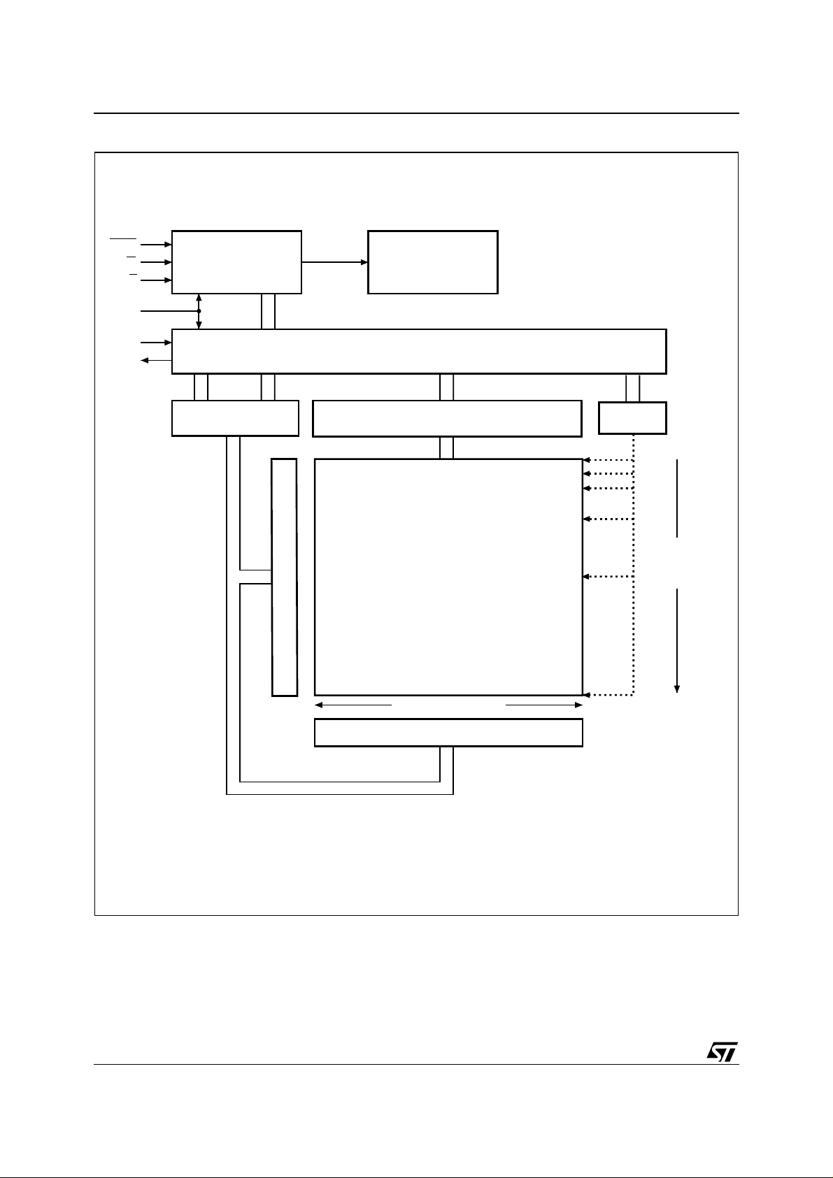
Figure 8. Block Diagram
HOLD
W
S
C
D
Q
Control Logic
Address Register
and Counter
Y Decoder
High Voltage
Generator
I/O Shift Register
256 Byte
Data Buffer
Status
Register
FFFFFh
Size of the
read-only
memory area
12/41
00000h
000FFh
256 Bytes (Page Size)
X Decoder
AI04987
INSTRUCTIONS
All instructions, addresses and data are shifted in
and out of the device, most significant bit first.
Serial Data Input (D) is sampled on the first rising
edge of Serial Clock (C) after Chip Select (S
) is
driven Low. Then, the one-byte instruction code
must be shifted in to the device, most significant bit
first, on Serial Data Input (D), each bit being
latched on the rising edges of Serial Clock (C).
The instruction set is listed in Tab le 4..
Every instruction sequence starts with a one-byte
instruction code. Depending on the instruction,
this might be followed by address bytes, or by data
bytes, or by both or none.
In the case of a Read Data Bytes (READ), Read
Data Bytes at Higher Speed (Fast_Read), Read
Status Register (RDSR) or Release from Deep
Power-down, and Read Electronic Signature
(RES) instruction, the shifted-in instruction se-
Table 4. Instruction Set
Instruction Description One-byte Instruction Code
WREN Write Enable 0000 0110 06h 0 0 0
quence is followed by a data-out sequ ence. Chip
Selec t (S
) can be driven High after any bit of the
data-out sequence is being shifted out.
In the case of a Page Program (PP), Sector Erase
(SE), Bulk Erase (BE), Write Status Register
(WRSR), Write Enable (WREN), Write Disable
(WRDI) or Deep Power-down (DP) instruction,
Chip Sele ct (S
) must be driven High exactly at a
byte boundary, otherwise the instruction is rejected, and is not executed. That is, Chip Select (S
must driven High when the number of clock pulses
after Chip Select (S
) being driven Low is an exact
multiple of eight.
All attempts to access the memory array during a
Write Status Register cycle, Program cycle or
Erase cycle are ignored, and the internal Write
Status Register cycle, Program cycle or Erase cycle continues unaffected.
Address
Bytes
Dummy
Bytes
M25P80
)
Data
Bytes
WRDI Write Disable 0000 0100 04h 0 0 0
RDSR Read Status Register 0000 0101 05h 0 0 1 to
WRSR Write Status Register 0000 0001 01h 0 0 1
READ Read Data Bytes 0000 0011 03h 3 0 1 to
FAST_READ Read Data Bytes at Higher Speed 0000 1011 0Bh 3 1 1 to ∞
PP Page Program 0000 0010 02h 3 0 1 to 256
SE Sector Erase 1101 1000 D8h 3 0 0
BE Bulk Erase 1100 0111 C7h 0 0 0
DP Deep Power-down 1011 1001 B9h 0 0 0
RES
Release from Deep Power-down,
and Read Electronic Signature
Release from Deep Power-down 0 0 0
1010 1011 ABh
0 3 1 to
∞
∞
∞
13/41

M25P80
Write Enable (WREN)
The Write Enable (WREN) instruction ( Figure 9.)
sets the Write Enable Latch (WEL) bit.
The Write Enable Latch (WEL) bit must be set prior to every Page Program (PP), Sector Erase
(SE), Bulk Erase (BE) and Write Status Register
(WRSR) instruction.
The Write Enable (WREN) instruction is entered
by driving Chip Select (S
struction code, and then driving Chip Select (S
High.
Figure 9. Write Enable (WREN) Instruction Sequence
S
0
21 34567
C
Instruction
D
High Impedance
Q
Write Disable (WRDI)
The Write Disable (WRDI) instruction (Figure 10. )
resets the Write Enable Latch (WEL) bit.
–Power-up
– Write Disable (WRDI) instruction completion
– Write Status Register (WRSR) instruction
The Write Disable (WRDI) instruction is entered by
driving Ch ip Select (S
tion code, and then driving Chip Select (S
The Write Enable Latch (WEL) bit is reset under
the following conditions:
) Low, sending the instruc-
) High.
– Page Program (PP) instruction completion
– Sector Erase (SE) instruction completion
– Bulk Erase (BE) instruction completion
) Low, sending the in-
)
AI02281E
completion
Figure 10. Write Disable (WRDI) Instruction Sequence
S
0
21 34567
C
Instruction
D
High Impedance
Q
14/41
AI03750D

M25P80
Read Status Register (RDSR)
The Read Status Register (RDSR) instruction allows the Status Register to be read. The Status
Register may be read at any time, even while a
Program, Erase or Write Status Register cycle is in
progress. When one of these cycles is i n progress,
it is recommended to check the Write In Progress
(WIP) bit before sending a new instruction to the
device. It is also possible to read the Status Register continuously, as shown in Figure 11..
Table 5. Status Register Format
b7 b0
SRWD 0 0 BP2 BP1 BP0 WEL WIP
Status Register
Write Protect
Block Protect Bits
Write Enable Latch Bit
Write In Progress Bit
The status and control bits of t he Status Register
are as follows:
WIP bit. The Write In Progress (WIP) bit indicates
whether the memory is busy with a Write Status
Register, Program or Erase cycle. When set to 1,
such a cycle is in progress, when reset to 0 no
such cycle is in progres s.
WEL bit. The Write Enable Latch (WEL) bit i ndicates the status of the internal Write Enable Latch.
When set to 1 the internal Write Enable Latch is
set, when set to 0 t he i nternal Write Enable Latch
is reset and no Write Status Register, Program or
Erase instruction is accepted.
BP2, BP1, BP0 bits. The Block Protect (BP2,
BP1, BP0) bits are non-volatile. They define the
size of the area to be software protected against
Program and Erase instructions. These bits are
written with the Write Status Register (WRSR) instruction. When one or both of the Block P rotect
(BP2, BP1 , BP0) bit s is s et to 1, the r ele vant m emory area (as defined in Table 2.) becomes protected against Page Program (PP) and Sector Erase
(SE) instructions. The Block Protect (BP2, BP1,
BP0) bits can be written provided that the Hardware Protected mode has not been set. T he Bulk
Erase (BE) instruction is executed if, and only if,
both Block Protect (BP2, BP1, BP0) bits are 0.
SRWD bit. The Status Register Write Disable
(SRWD) bit is operated in conjunction with the
Write Protect (W
) signal. The Status Register
Write Disable (SRWD) bit an d Write Protect (W
signal allow the device to be put in the Hardware
Protected mode (when t he Status Register Write
Disable (SRWD) bit is set to 1, and Write Protect
) is driven Low). In this mode, the non-volatile
(W
bits of the Status Register (SRWD, BP2, BP1,
BP0) become read-only bi ts and t he Write S tatus
Register (WRSR) instruction is no longer accepted
for execution.
)
Figure 11. Read Status Register (RDSR) Instruction Sequence and Data-Out Sequence
S
21 3456789101112131415
0
C
Instruction
D
Q
High Impedance
Status Register Out
7 6543210
MSB
Status Register Out
7 6543210
MSB
7
AI02031E
15/41

M25P80
Write Status Register (WRSR)
The Write Status Register (WRSR) instruction allows new values to be written to the Status Register. Before it can be accepted, a Write Enable
(WREN) instruction must previously have been executed. After the Write Enable (WREN) instruction
has been decoded and ex ecuted, the device sets
the Write Enable Latch (WEL).
The Write Status Register (WRSR) instruction is
entered by driving Chip Select (S
) Low, followed
by the instruction code and the data byte on Serial
Data Input (D).
The instruction sequence is shown in Figure 12..
The Write Status Register (WRSR) instruction has
no effect on b6, b5, b1 and b0 of the Status Register. b6 and b5 are always read as 0.
Chip Select (S
) must be driven High after the
eighth bit of the d ata byte has been latched in. If
not, the Write Status Register (WRSR) instruction
is not executed. As soon as Chip Select (S
) is driv-
en High, the se lf-timed Wri te Statu s Regist er cycl e
(whose duration is t
Status Register cycle is in progress, the Status
Register may still be read to check the value of the
Write In Progress (WIP) bit. The Write In Progress
(WIP) bit is 1 during the self-timed Write Status
Register cycle, and is 0 when it is completed.
When the cycle is completed, the Write Enable
Latch (WEL) is reset.
The Write Status Register (WRSR) instruction allows the user to change the values of the Block
Protect (BP2, BP1, BP0) bits, to define the size of
the area that is to be treated as read-only, as defined in Table 2.. The Write Status Register
(WRSR) instruction also allows the user to set or
reset the Status Register Write Disable (SRWD)
bit in accordance with the Write Protect (W
The Status Register Write Disable (SRWD) bit and
Write Protect (W
in the Hardware Protected Mode (HPM). The Write
Status Register (WRSR) instruction is not executed once the Hardware P rotected Mode (HPM) is
entered.
Figure 12. Write Status Register (WRSR) Instruction Sequence
) is initiated. While the Writ e
W
) signal.
) signal allow the device to be put
S
21 3456789101112131415
0
C
Instruction Status
D
High Impedance
Q
765432 0
MSB
Register In
1
AI02282D
16/41

Table 6. Protection Modes
W
SRWD
Signal
10
00
11
01
Note: 1. As defined by th e values in the Blo ck Protect (BP2, BP1, BP0) bits of the Statu s R egi ster, as shown in Table 2..
Bit
Mode
Software
Protected
(SPM)
Hardware
Protected
(HPM)
The protection features of the device are summarized in Table 6..
When the Status Register Write Disable (SRWD)
bit of the Status Register is 0 (its initial delivery
state), it is possible to write to the Status Register
provided that the Write Enable Latch (WEL) bit has
previously been set by a Write Enable (WREN) instruction, regardless of th e whether W rite Prote ct
) is driven High or Low.
(W
When the Status Register Write Disable (SRWD)
bit of the Status Register is set to 1, two cases
need to be considered, depending on the st ate of
Write Protect (W
– If Write Protect (W
):
) is driven High, it is
possible to write to the Status Register
provided that the Write Enable Latch (WEL) bit
has previously been set by a Write Enable
(WREN) instruction.
– If Write Protect (W
) is driven Low, it is not
possible to write to the Status Register even if
the Write Enable Latch (WEL) bit has
previously been set by a Write Enable
(WREN) instruction. (Attempts to write to the
Write Protection of the
Status Register
Status Register is Writable
(if the WREN instruction
has set the WEL bit)
The values in the SRWD,
BP2, BP1 and BP0 bits
can be changed
Status Register is
Hardware write protected
The values in the SRWD,
BP2, BP1 and BP0 bits
cannot be changed
Protected Area
Protected against Page
Program, Sector Erase
and Bulk Erase
Protected against Page
Program, Sector Erase
and Bulk Erase
Status Register are rejected, and are not
accepted for execution). As a consequence,
all the data bytes in the memory area that are
software protected (SPM) by the Block Protect
(BP2, BP1, BP0) bits of the Status Register,
are also hardware protected against data
modification.
Regardless of the order of the two events, the
Hardware Protected Mode (HPM) can be entered:
– by setting the Status Register Write Disable
(SRWD) bit after driving Write Protect (W
– or by driving Write Protect (W
setting the Status Register Write Disable
(SRWD) bit.
The only way to exit the Hardware Protected Mode
(HPM) once entered is to pull W rite Protect (W
High.
If Write Protect (W
Hardware Protected Mode (HPM) can never be
activated, and only t he Software Protec ted Mode
(SPM), using the Block Protect (BP2, BP1, BP0)
bits of the Status Register, can be used.
Memory Content
1
Unprotected Area
Ready to accept Page
Program and Sector Erase
instructions
Ready to accept Page
Program and Sector Erase
instructions
) Low after
) is permanently tied High, t he
M25P80
1
) Low
)
17/41

M25P80
Read Data Bytes (READ)
The device is first selected by driving Chip Select
(S
) Low. The instruction code for the Read Data
Bytes (READ) instruction is followed by a 3-byte
address (A23-A0), each bit being latched-in during
the rising edge of Serial Clock (C). Then the memory contents, at that address, is shifted out on Serial Data Output (Q), each bit being shifted out, at
a maximum frequency f
, during the falling edge of
R
Serial Clock (C).
The instruction sequence is shown in Figure 13..
The first byte addressed can be at any location.
The address is automatically incremented to the
next higher address after each byte of data is shift ed out. The whole memory can, therefore, be read
with a single Read Data Bytes (READ) i nst ruction.
When the highest address is reached, the address
counter rolls over to 000000h, allowing the read
sequence to be continued indefinitely.
The Read Data Bytes (READ) instruction is terminated by driving Chip Select (S
) can be driven High at any time during data out-
(S
) High. Chip Select
put. Any Read Data Bytes (READ) instruction,
while an Erase, Program or Write cycle is in
progress, is rejected without having any effects on
the cycle that is in progr ess .
Figure 13. Read Data Bytes (READ) Instruction Sequence and Data-Out Sequence
S
21 345678910 2829303132333435
0
C
Instruction 24-Bit Address
36 37 38
39
D
High Impedance
Q
Note: Address bits A23 to A20 are Don’t Care.
23
2221 3210
MSB
Data Out 1
76543 1 7
MSB
2
0
Data Out 2
AI03748D
18/41

M25P80
Read Data Bytes at Higher Speed (FAST_READ)
The device is first selected by driving Chip Select
) Low. The instruction code for the Read Data
(S
Bytes at Higher Speed (FAST_READ) i nstruction
is followed by a 3-byte address (A23-A0) and a
dummy byte, each bit being latc hed-in during the
rising edge of Serial Clock (C). Then the memory
contents, at that address, is shifted out on Serial
Data Output (Q), each bit being shif ted out, at a
maximum frequency f
, during the falling edge of
C
Serial Clock (C).
The instruction sequence is shown in Figure 14..
The first byte addressed can be at any location.
The address is automatically incremented to the
next higher address after each byte of data is shift ed out. The whole memory can, therefore, be read
with a single Read Data Bytes at Higher Speed
(FAST_READ) instruction. When the highest address is reached, the address counter rolls over to
000000h, allowing the read sequence to be continued indefinitely.
The Read Data Bytes at Higher Speed
(FAST_READ) instruction is terminated by driving
Chip Select (S
) High. Chip Select (S) can be driven High at any time during data output. Any Read
Data Bytes at Higher Speed (FAST_READ) instruction, while an Erase, Program or Write cycle
is in progress, is rejected without having any effects on the cycle that is in progress.
Figure 14. Read Data Bytes at Higher Speed (FAST_READ) Instruction Sequence and Data-Out Sequence
S
21 345678910 28293031
0
C
Instruction 24 BIT ADDRESS
23
D
High Impedance
Q
S
32 33 34 36 37 38 39 40 41 42 43 44 45 46
C
D
Q
765432 0
35
Dummy Byte
2221 3210
1
DATA OUT 1
765432 0
MSB
47
DATA OUT 2
7 6543210
1
MSB MSB
7
AI04006
Note: Address bits A23 to A20 are Don’t Care.
19/41

M25P80
Page Program (PP)
The Page Program (PP) instruction allows bytes to
be programmed in the memory (changing bits from
1 to 0). Before it can be accepted, a Wri te Enab le
(WREN) instruction must previously have been executed. After the Write Enable (WREN) instruction
has been decoded, the device sets the Write Enable Latch (WEL).
The Page Program (PP) instruction is ent ered by
driving Chip Select (S
) Low, followed by the instruction code, three address by tes and at least
one data byte on Serial Data Input (D). If the 8
least significant address bits (A7-A0) are not all
zero, all transmitted data that goes beyond the end
of the current page are programmed from the start
address of the same page (from the address
whose 8 least significant bits (A7-A0) are all zero).
Chip Selec t (S
) must be driven Low for the entire
duration of the sequence.
The instruction sequence is shown in Figure 15..
If more than 256 bytes are sent to the device, pre-
viously latched data are discarded and the last 256
data bytes are guaranteed to be programmed cor-
Figure 15. P age P rog ra m (P P) Ins truction Sequence
rectly within the same page. If less t han 2 56 Dat a
bytes are sent to device, they are correc tl y programmed at the requested addresses without having any effects on the other bytes of the same
page.
Chip Select (S
) must be driven High after the
eighth bit of the last data byte has been latched in,
otherwise the Page Program (PP) instruction is not
executed.
As soon as Chip Select (S
timed Page Pr ogram cycle (whose duratio n is t
) is dr iv en Hi gh, the s elf -
PP
is initiated. While the Page Program cycle is in
progress, the Status Register may be read to
check the value of the Write In Progress (WIP) bit.
The Write In Progress (WIP) bit is 1 during the selftimed Page Program cycle, and is 0 when it is
completed. At some unspecified time before the
cycle is completed, the Write Enable Latch (WEL)
bit is reset.
A Page Program (PP) instruction applied to a page
which is protected by the Block Protect (BP2, BP1,
BP0) bits (see Table 3. and Table 2.) is no t ex ec ut-
ed.
)
S
21 345678910 2829303132333435
0
C
Instruction 24-Bit Address
23
D
S
4241 43 44 45 46 47 48 49 50 52 53 54 5540
C
Data Byte 2
D
765432 0
MSB MSB MSB
1
2221 3210
MSB
51
Data Byte 3 Data Byte 256
765432 0
1
765432 0
MSB
2072
765432 0
36 37 38
Data Byte 1
2075
2074
2073
2076
1
2077
1
39
2079
2078
AI04082B
Note: Address bits A23 to A20 are Don’t Care.
20/41

M25P80
Sector Erase (SE)
The Sector Erase (SE) instruction sets t o 1 (FFh)
all bits inside the chosen sector. Before it ca n be
accepted, a Write Enable (WREN) instruction
must previously have been executed. After the
Write Enable (WREN) instruction has been decoded, the device sets the Write Enable Latch (WEL).
The Sector Erase (SE) instruction is entered by
driving Chip Select (S
) Low, followed by the instruction code, and three address by tes on Serial
Data Input (D). Any address inside the Sector (see
Table 3.) is a valid address for the Sector Erase
(SE) instruction. Chip Select (S
) must be driven
Low for the entire duration of the sequence.
The instruction sequence is shown in Figure 16..
Figure 16. Sector Erase (SE) Instruction Sequ ence
S
21 3456789 293031
0
C
Chip Select (S
) must be driven High after the
eighth bit of the last address byte has been latched
in, otherwise the S ector Erase (SE) i nstruction is
not executed. As soon as Chip Select (S
) is driven
High, the self -timed Sector Erase cycle (whose duration is t
) is initiated. While the Sector Erase cy-
SE
cle is in progress, the Status Register may be read
to check the value of the Write In Progress (WIP)
bit. The Write In Progress (WIP) bit is 1 during the
self-timed Sector Erase cycle, and is 0 when it is
completed. At some unspecified time before the
cycle is completed, the Write Enable Latch (WEL)
bit is reset.
A Sector Erase (SE) instruction applied to a page
which is protected by the Block Protect (BP2, BP1,
BP0) bits (see Table 3. and Table 2.) is no t ex ec ut-
ed.
D
Note: Address bits A23 to A20 are Don’t Care.
Instruction
24 Bit Address
23 22 2 0
MSB
1
AI03751D
21/41

M25P80
Bulk Erase (BE)
The Bulk Erase (BE) instruction sets all bits to 1
(FFh). Before it can be accepted, a Write Enab le
(WREN) instruction must previously have been executed. After the Write Enable (WREN) instruction
has been decoded, the device sets the Write Enable Latch (WEL).
The Bulk Erase (BE) instruction is entered by driving Chip Select (S
code on Serial Data Input (D). Chip Select (S
) Low, followed by the instruction
)
must be driven Low for the entire duration o f the
sequence.
The instruction sequence is shown in Figure 17..
Chip Select (S
) must be driven High after the
eighth bit of the instruction code has been latched
Figure 17. Bulk Erase (BE) Instruction Sequence
S
21 345670
C
in, otherwise the Bulk Erase instruction is not executed. As soon as Chip Select (S
) is driven High,
the self-timed Bu l k Era se cycle (whose duration is
) is initiated. While the Bulk Erase cycle is in
t
BE
progress, the Status Register may be read to
check the value of the Write In Progress (WIP) bit.
The Write In Progress (WIP) bit is 1 during the selftimed Bulk Erase cycle, and is 0 when it is completed. At some unspecified time before the cycle
is completed, the Write Enable Latch (WEL) bit is
reset.
The Bulk Erase (BE) instruction is executed only if
all Block Prote ct (BP2, BP1, BP0) bits are 0. The
Bulk Erase (BE) instruction is ignored if one, or
more, sectors are protected.
Instruction
D
AI03752D
22/41

M25P80
Deep Power-down (DP)
Executing the Deep Power-down (DP) instruction
is the only way to put the device in the lowest consumption mode (the Deep Power-down mode). It
can also be used as an extra s oftware protection
mechanism, while the device is not in active use,
since in this mod e, the device ignores all Write,
Program and Erase instructions.
Driving Chip Select (S
) High deselects the device,
and puts the device in the S tandby m ode (if t here
is no internal cycle currently in progress). But this
mode is not the Deep Power-down mode. The
Deep Power-down mode can onl y be entered by
executing the Deep Power-down (DP ) instruction,
to reduce the standby current (from I
CC1
to I
CC2
as specified in Table 12.).
Once the device has entered the Deep Power-
down mode, all instructions are ignored except the
Release from Deep Power-down and Read Electronic Signature (RES) instruction. This releases
the device from this mode. The Release from
Deep Power-down and Read Electronic Signature
(RES) instruction also allows the Electronic Signa-
ture of the device to be out put on Serial Data Output (Q).
The Deep Power-down m ode automatically stops
at Power-down, and the device always Powers-up
in the Standby mode.
The Deep Power-down (DP) instruction is entered
by driving Chip Select (S
struction code on Serial Data Input (D). Chip Select (S
of the sequence.
The instruction sequence is shown in Figure 18..
Chip Select (S
eighth bit of the instruction code has been latched
in, otherwise the Deep Power-down (DP) instruc-
,
tion is not executed. As soon as Chip Select (S
driven High, it requires a delay of t
supply current is reduced to I
Power-down mode is entered.
Any Deep Power-down (DP) instruction, while an
Erase, Program or Write cycle is in progress, is rejected without havi n g any effects on the cycle that
is in progress.
Figure 18. Deep Power-down (DP) Instruction Sequence
) Low, followed by the in-
) must be driven Low for the entire duration
) must be driven High after the
) is
before the
DP
and the Deep
CC2
S
t
21 345670
C
Instruction
D
DP
Stand-by Mode
Deep Power-down Mode
AI03753D
23/41

M25P80
Release from Deep Power-down and Read Electronic Signature (RES)
Once the device has entered the Deep Powerdown mode, all instructions are ignored except the
Release from Deep Power-down and Read Electronic Signature (RES) instruction. Executing this
instruction takes the device out of the Deep Power-down mode.
The instruction can also be used to read, on Serial
Data Output (Q), the 8-bit Electronic Signature,
whose value for the M25P80 is 13h.
Except while an Erase, P rogram or Write Status
Register cycle is in progress, the Release from
Deep Power-down and Read Electronic Signature
(RES) instruction always provides access to the 8bit Electronic Signature of the device, and can be
applied even if the Deep Power-down mode has
not been entered.
Any Release from Deep Power-down and Read
Electronic Signature (RES) instruction while an
Erase, Program or Write Status Register cycle is in
progress, is not decoded, and has no effect on the
cycle that is in progress.
The device is first selected by driving Chip Select
) Low. The instruction code is followed by 3
(S
dummy bytes, each bit being latched-in on Serial
Data Input (D) during the rising edge of Serial
Clock (C). Then, the 8-bit Electronic Signature,
stored in the memory, is shifted out on Serial Data
Output (Q), each bit being shifted out d uring the
falling edge of Serial Clock (C).
The instruction sequence is shown in Figure 19..
The Release from Deep Power-down and Read
Electronic Signature (RES) instruction is terminated by driving Chip Select (S
) High after the Electronic Signature has been read at least once.
Sending additional clock cycles on Serial Clock
(C), while Chip Select (S
) is driven Low, cause the
Electronic Signature to be output repeatedly.
When Chip Select (S
) is driven High, the device i s
put in the Stand-by Power mode. If the device was
not previously in the Deep Power-down mode, the
transition to the Stand-by Pow er m ode is immediate. If the device was previously in the Deep Power-down mode, though, the transition to the Standby Power mode is delayed by t
) must remain High for at least t
lect (S
, and Chip Se-
RES2
RES2
(max),
as specified in Table 17.. Once in the Stand-by
Power mode, the device waits to be selected, so
that it can receive, decode and execute instructions.
Figure 19. Release from Deep Power-d ow n and Read Electronic Signatur e (RES) Instructi on
Sequence a n d D a ta -O u t Se quence
S
21 345678910 2829303132333435
0
C
Instruction 3 Dummy Bytes
23
D
High Impedance
Q
Note: T he value of the 8-bit Electro ni c S i gnature, for the M25P80, is 13h.
2221 3210
MSB
Electronic Signature Out
765432 0
MSB
Deep Power-down Mode
36 37 38
1
t
RES2
Stand-by Mode
AI04047C
24/41

Figure 20. Release from Deep Power-d ow n (RES) Instruction Sequen ce
S
t
21 345670
C
Instruction
D
High Impedance
Q
RES1
M25P80
Driving Chip Select (S
) High after the 8-bit instruction byte has been received by the device, but before the whole of the 8-bit Electronic Signature has
been transmitted for the first time (as shown in Fig-
ure 20.), still insures that the device is put into
Stand-by Power mode. If the d evice was not previously in the Deep Power-down mode, the transition to the Stand-by Power mode is immediate. If
Deep Power-down Mode
Stand-by Mode
AI04078B
the device was previously in the Deep Powerdown mode, though, the transition to the Stand-by
Power mode is delayed by t
) must remain High for at least t
(S
, and Chip Select
RES1
RES1
(max), as
specified in Table 17.. Once in the Stand-by Power
mode, the device waits to be selected, so that it
can receive, decode and execute instructions.
25/41

M25P80
POWER-UP AND POWER-DOWN
At Power-up and Power-down, the device must
not be selected (that is Chip Select (S
the voltage applied on V
) unt i l VCC reaches the
CC
correct value:
–V
(min) at Power-up, and then for a further
CC
delay of t
VSL
–VSS at Power-down
Usually a simple pull-up resistor on Chip Select (S
can be used to insure safe and proper Power-up
and Power-down.
To avoid data corruption and inadvertent write operations during power up, a Power On Reset
(POR) circuit is included. Th e logic inside the device is held reset w hile V
threshold value, V
– all operations are disabled,
WI
is less than the POR
CC
and the device does not respond to any instruction.
Moreover, the device ignores all Write Enable
(WREN), Page Program (PP), Sector Erase (SE),
Bulk Erase (BE) and Write Status Register
(WRSR) instructions until a time delay of t
elapsed after the moment that V
threshold. However, the correct operation of
V
WI
the device is not guaranteed if, by this time, V
still below V
(min). No Write Status Register,
CC
) must follow
rises above the
CC
PUW
has
CC
is
Program or Erase instructions should be sent until
the later of:
–t
–t
after VCC passed the VWI threshold
PUW
afterVCC passed the VCC(min) level
VSL
These values are specified in Table 7..
If the delay, t
above V
)
READ instructions even if the t
CC
, has elapsed, after VCC has risen
VSL
(min), the device can be selected for
delay is not yet
PUW
fully elapsed.
At Power-up, the device is in the following state:
– The device is in the Standby mode (not the
Deep Power-down mode).
– The Write Enable Latch (WEL) bit is reset.
Normal precautions must be taken for supply rail
decoupling, to stabilize the V
in a system should have the V
feed. Each device
CC
rail decoupled by
CC
a suitable capacitor close to the package pins.
(Generally, this capacitor is of the order of 0.1µF).
At Power-down, when V
drops from the operat-
CC
ing voltage, to below the POR threshold value,
, all operations are disabled and the device
V
WI
does not respond to any instruction. (The designer
needs to be aware that if a Power-down occurs
while a Write, Program or Erase cycle is in
progress, some data corruption can result.)
26/41

Figure 21. Power-up Timing
V
CC
VCC(max)
Program, Erase and Write Commands are Rejected by the Device
Chip Selection Not Allowed
VCC(min)
M25P80
Reset State
of the
Device
V
WI
Table 7. Power-Up Timing and V
Threshol d
WI
tVSL
tPUW
Read Access allowed Device fully
accessible
time
AI04009C
Symbol Parameter Min. Max. Unit
1
t
VSL
t
PUW
V
Note: 1. These param eters are characterized onl y.
VCC(min) to S low
1
Time delay to Write instruction 1 10 ms
1
Write Inhibit Voltage 1 2 V
WI
10 µs
INITIAL DELIVERY STATE
The device is delivered with the memory array
erased: all bits are set to 1 (each byte contains
FFh). The Status Register contains 00h (all Status
Register bits are 0).
27/41

M25P80
MAXIMUM RA T ING
Stressing the device above the rating listed in the
Absolute Maximum Ratings" table may cause permanent damage to the device. These are stress
ratings only and operation of the device at t hese or
any other conditions ab ove those i ndicated in t he
Operating sections of this specificat ion is not im-
Table 8. Absolute Maximum Ratings
Symbol Parameter Min. Max. Unit
T
T
STG
LEAD
Storage Temperature –65 150 °C
Lead Temperature during Soldering
plied. Exposure to Absolute Maximum Rating conditions for extended periods may affect device
reliability. Refer also to the STMicroelectronics
SURE Program and other relevan t quality documents.
See note
1
°C
V
IO
V
CC
V
ESD
Note: 1. Compliant wit h JED EC Std J- ST D-020 B (for small body, Sn-P b or Pb asse mbl y), the ST EC OPACK® 71913 95 specification, and
the European directive on Restrictions on Hazardous Substances (RoHS) 200 2/ 95/EU
2. JED EC St d JESD22-A114A (C1=100 pF, R1 =1500
Input and Output Voltage (with respect to Ground) –0.6 4.0 V
Supply Voltage –0.6 4.0 V
Electrostatic Discharge Voltage (Human Body model)
Ω, R2=500 Ω)
2
–2000 2000 V
28/41

DC AND AC PARAMETERS
This section summarizes the operating and measurement conditions, and the DC and AC characteristics of the device. The parameters in the DC
and AC Characteristic tables that follow are derived from tests performed under the Measure-
Table 9. Operating Conditions
Symbol Parameter Min. Max. Unit
ment Conditions summarized in the relevant
tables. Designers should check that the operating
conditions in their circuit match t he measurem ent
conditions when relying on the quoted parameters.
M25P80
V
CC
T
A
Supply Voltage 2.7 3.6 V
Ambient Operating Temperature (Device Grade 6) –40 85
Ambient Operating Temperature (Device Grade 3) –40 125
Table 10. Data Retentio n a nd En durance
Parameter Condition Min. Max. Unit
Device Grade 6 100 000
Erase/Program Cycles
Device Grade 3
Device Grade 6 20
Data Retention
Device Grade 3
Note: 1. This is preliminary data
1
1
(at 85°C)
10 000
20
Table 11. Capacitance
Symbol Parameter Test Condition Min. Max. Unit
C
OUT
C
IN
Note: S ampled only, not 100% tested, at TA=25°C an d a frequency of 20M Hz.
Output Capacitance (Q) V
Input Capacitance (other pins) VIN = 0V 6 pF
= 0V 8 pF
OUT
°C
cycles per
sector
years
29/41

M25P80
Table 12. DC Characteristics (Device Grade 6)
Symbol Parameter
Input Leakage Current ± 2 µA
I
LI
I
Output Leakage Current ± 2 µA
LO
I
I
I
I
I
I
I
V
V
V
Standby Current
CC1
Deep Power-down Current
CC2
Operating Current (READ)
CC3
Operating Current (PP)
CC4
Operating Current (WRSR) S = V
CC5
Operating Current (SE) S = V
CC6
Operating Current (BE) S = V
CC7
V
Input Low Voltage –0.5
IL
Input High Voltage
IH
Output Low Voltage
OL
Output High Voltage IOH = –100µAV
OH
(in addition to those in Table 9.)
S
= VCC, V
S
= VCC, V
C=0.1V
C=0.1V
Test Condition
= VSS or V
IN
= VSS or V
IN
/ 0.9.VCC at 40MHz,
CC
Q = open
/ 0.9.VCC at 20MHz,
CC
Q = open
S
= V
CC
CC
CC
CC
I
= 1.6mA
OL
CC
CC
Min. Max. Unit
50 µA
10 µA
8mA
4mA
15 mA
15 mA
15 mA
15 mA
0.3V
CC
0.7V
CCVCC
+0.4
0.4 V
–0.2 V
CC
V
V
Table 13. DC Characteristics (Device Grade 3)
Symbol Parameter
Input Leakage Current ± 2 µA
I
LI
I
Output Leakage Current ± 2 µA
LO
I
I
I
I
I
I
I
V
V
V
Note: 1. This is preliminary data
Standby Current S = VCC, V
CC1
Deep Power-down Current
CC2
Operating Current (READ)
CC3
Operating Current (PP) S = V
CC4
Operating Current (WRSR)
CC5
Operating Current (SE)
CC6
Operating Current (BE) S = V
CC7
V
Input Low Voltage – 0.5 0.3V
IL
Input High Voltage 0.7V
IH
Output Low Voltage IOL = 1.6mA 0.4 V
OL
Output High Voltage
OH
(in addition to those in Table 9.)
S
= VCC, V
C=0.1V
C=0.1V
Test Condition
= VSS or V
IN
= VSS or V
IN
/ 0.9.VCC at 40MHz,
CC
CC
CC
Min.
1
Q = open
/ 0.9.VCC at 20MHz,
CC
Q = open
CC
S
= V
CC
S
= V
CC
CC
CCVCC
I
= –100µAV
OH
CC
–0.2
1
Max.
Unit
100 µA
50 µA
8mA
4mA
15 mA
15 mA
15 mA
15 mA
V
CC
+0.4 V
V
30/41

M25P80
Table 14. Instruction Times (Device Gra de 6)
Test conditions specified in Table 9. and Table 16.
Symbol Alt. Parameter Min. Typ. Max. Unit
t
W
t
PP
t
SE
t
BE
Table 15. Instruction Times (Device Gra de 3)
Symbol Alt. Parameter Min.
t
W
t
PP
t
SE
t
BE
Note: 1. At 85°C
2. This is preliminary data
Write Status Register Cycle Time 5 15 ms
Page Program Cycle Time 1.4 5 ms
Sector Erase Cycle Time 1 3 s
Bulk Erase Cycle Time 10 20 s
Test conditions specified in Table 9. and Table 16.
Typ.
1,2
Max.
2
Write Status Register Cycle Time 8 15 ms
Page Program Cycle Time 1.5 5 ms
Sector Erase Cycle Time 1 3 s
Bulk Erase Cycle Time 10 20 s
Unit
Table 16. AC Measuremen t Condition s
Symbol Parameter Min. Max. Unit
C
L
Load Capacitance 30 pF
Input Rise and Fall Times 5 ns
to 0.8V
Input Pulse Voltages
Input Timing Reference Voltages
Output Timing Reference Voltages
Note: Output Hi- Z is def i ned as the point where data ou t is no longer driven.
0.2V
0.3V
CC
to 0.7V
CC
V
CC
CC
CC
/ 2
Figure 22. AC Measurement I/O W aveform
Input Levels
0.8V
CC
0.2V
CC
Input and Output
Timing Reference Levels
0.7V
CC
0.5V
CC
0.3V
CC
AI07455
V
V
V
31/41

M25P80
Table 17. AC Characteristics (25MHz Operati on, Device Grad e 6 or 3)
Test conditions specified in Table 9. and Table 16.
Symbol Alt. Parameter
Clock Frequency for the following instructions:
f
C
f
C
FAST_READ, PP, SE, BE, DP, RES,
WREN, WRDI, RDSR, WRSR
f
R
1
t
CH
1
t
CL
2
t
CLCH
2
t
CHCL
t
SLCH
t
CHSL
t
DVCH
t
CHDX
t
CHSH
t
SHCH
t
SHSL
2
t
SHQZ
t
CLQV
t
CLQX
t
HLCH
t
CHHH
t
HHCH
t
CHHL
2
t
HHQX
2
t
HLQZ
4
t
WHSL
4
t
SHWL
2
t
DP
2
t
RES1
2
t
RES2
Note: 1. tCH + tCL must be greater than or equal to 1/ f
2. Value guarantee d by characteri zation, not 100% tested in production.
3. Expressed as a slew-rate.
4. Only applicable as a constraint for a WRSR instruc tion when SRWD is set at 1.
5. For device grade 3, this is Prelimi nary Data
t
CLH
t
CLL
t
CSS
t
DSU
t
t
CSH
t
DIS
t
t
t
DH
t
V
HO
LZ
HZ
Clock Frequency for READ instructions D.C. 20 MHz
Clock High Time 18 ns
Clock Low Time 18 ns
Clock Rise Time3 (peak to peak)
Clock Fall Time3 (peak to peak)
S Active Setup Time (relative to C) 10 ns
S Not Active Hold Time (relative to C) 10 ns
Data In Setup Time 5 ns
Data In Hold Time 5 ns
S Active Hold Time (relative to C) 10 ns
S Not Active Setup Time (relative to C) 10 ns
S Deselect Time 100 ns
Output Disable Time 15 ns
Clock Low to Output Valid 15 ns
Output Hold Time 0 ns
HOLD Setup Time (relative to C) 10 ns
HOLD Hold Time (relative to C) 10 ns
HOLD Setup Time (relative to C) 10 ns
HOLD Hold Time (relative to C) 10 ns
HOLD to Output Low-Z 15 ns
HOLD to Output High-Z 20 ns
Write Protect Setup Time 20 ns
Write Protect Hold Time 100 ns
S High to Deep Power-down Mode 3 µs
S High to Standby Mode without Electronic
Signature Read
S High to Standby Mode with Electronic
Signature Read
C
Min.
D.C. 25 MHz
0.1 V/ns
0.1 V/ns
5
Typ.
Max.
5
Unit
3 µs
1.8 µs
32/41

Table 18. AC Characteristics (40MHz Operati on, Device Grad e 6)
40MHz available for products marked since week 20 of 2004, only
Test conditions specified in Table 9. and Table 16.
M25P80
5
Symbol Alt. Parameter
Clock Frequency for the following instructions:
f
C
f
C
FAST_READ, PP, SE, BE, DP, RES,
WREN, WRDI, RDSR, WRSR
f
R
1
t
CH
1
t
CL
2
t
CLCH
2
t
CHCL
t
SLCH
t
CHSL
t
DVCH
t
CHDX
t
CHSH
t
SHCH
t
SHSL
2
t
SHQZ
t
CLQV
t
CLQX
t
HLCH
t
CHHH
t
HHCH
t
CHHL
2
t
HHQX
2
t
HLQZ
4
t
WHSL
4
t
SHWL
2
t
DP
2
t
RES1
2
t
RES2
Note: 1. tCH + tCL must be greater than or equal to 1/ f
2. Value guarantee d by characteri zation, not 100% tested in production.
3. Expressed as a slew-rate.
4. Only applicable as a constraint for a WRSR instruc tion when SRWD is set at 1.
5. Detai l s of how to find the date of mark i ng are given in Ap pl i cation Note, AN1995.
t
CLH
t
CLL
t
CSS
t
DSU
t
t
CSH
t
DIS
t
t
t
DH
t
V
HO
LZ
HZ
Clock Frequency for READ instructions D.C. 20 MHz
Clock High Time 11 ns
Clock Low Time 11 ns
Clock Rise Time3 (peak to peak)
Clock Fall Time3 (peak to peak)
S Active Setup Time (relative to C) 5 ns
S Not Active Hold Time (relative to C) 5 ns
Data In Setup Time 2 ns
Data In Hold Time 5 ns
S Active Hold Time (relative to C) 5 ns
S Not Active Setup Time (relative to C) 5 ns
S Deselect Time 100 ns
Output Disable Time 9 ns
Clock Low to Output Valid 9 ns
Output Hold Time 0 ns
HOLD Setup Time (relative to C) 5 ns
HOLD Hold Time (relative to C) 5 ns
HOLD Setup Time (relative to C) 5 ns
HOLD Hold Time (relative to C) 5 ns
HOLD to Output Low-Z 9 ns
HOLD to Output High-Z 9 ns
Write Protect Setup Time 20 ns
Write Protect Hold Time 100 ns
S High to Deep Power-down Mode 3 µs
S High to Standby Mode without Electronic
Signature Read
S High to Standby Mode with Electronic
Signature Read
C
Min.
Typ.
Max.
Unit
D.C. 40 MHz
0.1 V/ns
0.1 V/ns
3 µs
1.8 µs
33/41

M25P80
Figure 23. Se ri al Input Timing
S
C
tDVCH
tSLCH
tSHSL
tCHSHtCHSL
tSHCH
tCHCL
tCHDX
D
Q
MSB IN
High Impedance
tCLCH
LSB IN
Figure 24. Wri t e Pr ot ec t Setup and Hold Ti m in g du rin g W RS R when SRWD=1
W
tWHSL
S
C
AI01447C
tSHWL
34/41
D
High Impedance
Q
AI07439

Figure 25. Hol d T im i ng
S
C
Q
D
HOLD
tCHHL
M25P80
tHLCH
tHHCH
tCHHH
tHHQXtHLQZ
AI02032
Figure 26. Out put Timing
S
C
tCLQV
tCLQX
Q
ADDR.LSB IN
D
tCLQX
tCLQV
tCH
tCL
tQLQH
tQHQL
tSHQZ
LSB OUT
AI01449D
35/41

M25P80
PACKAG E MECHANICAL
Figure 27. VDFPN8 (MLP8) 8-lead Very thin Dual Flat Package No lead, Package Outline
D
D1
E
E1
eE2
b
A
Note: Drawing is not to scale.
θ
A2
A3A1
D2
L
VDFPN-01
Table 19. VDFPN8 (MLP8) 8-lead Very thin Dual Flat Package No lead, Package Mechan ical Data
Symb.
Typ. Min. Max. Typ. Min. Max.
A 0.85 1.00 0.0335 0.0394
A1 0.00 0.05 0.0000 0.0020
A2 0.65 0.0256
A3 0.20 0.0079
b 0.40 0.35 0.48 0.0157 0.0138 0.0189
D 6.00 0.2362
D1 5.75 0.2264
D2 3.40 3.20 3.60 0.1339 0.1260 0.1417
mm inches
36/41
E 5.00 0.1969
E1 4.75 0.1870
E2 4.00 3.80 4.20 0.1575 0.1496 0.1654
e 1.27 0.0500
L 0.60 0.50 0.75 0.0236 0.0197 0.0295
θ 12° 12°

M25P80
Figure 28. SO16 wide – 16-lead Plastic Small Outline, 300 mils body width, Package Outline
D
16
1
9
E
8
A2
H
A
h x 45˚
LA1
ddd
B
e
SO-H
Note: Drawing is not to scale.
Table 20. SO16 wide – 16-lead Plastic Small Outline, 300 mils body width, Mechanica l Data
Symb.
Typ. Min. Max. Typ. Min. Max.
mm inches
C
θ
A 2.35 2.65 0.093 0.104
A1 0.10 0.30 0.004 0.012
B 0.33 0.51 0.013 0.020
C 0.23 0.32 0.009 0.013
D 10.10 10.50 0.398 0.413
E 7.40 7.60 0.291 0.299
e1.27––0.050––
H 10.00 10.65 0.394 0.419
h 0.25 0.75 0.010 0.030
L 0.40 1.27 0.016 0.050
q0808
ddd 0.10 0.004
37/41

M25P80
Figure 29. SO8 wide – 8 lead Plastic Small Outline, 200 mils bod y width, Pac kage Ou tline
Note: Drawing is not to scale.
A2
B
e
D
N
1
SO-b
CP
E
H
A
C
LA1 α
Table 21. SO8 wide – 8 lead Plastic Small Outline, 200 mils body width, Package Mec hanica l Data
Symb.
Typ. Min. Max. Typ. Min. Max.
A 2.03 0.080
A1 0.10 0.25 0.004 0.010
A2 1.78 0.070
mm inches
38/41
B 0.35 0.45 0.014 0.018
C 0.20 – – 0.008 – –
D 5.15 5.35 0.203 0.211
E 5.20 5.40 0.205 0.213
e1.27––0.050––
H 7.70 8.10 0.303 0.319
L 0.50 0.80 0.020 0.031
α 0° 10° 0° 10°
N8 8
CP 0.10 0.004

PART NUMBERING
Table 22. Ordering Information Scheme
Example: M25P80 – V MF 6 T P
Device Type
M25P = Serial Flash Memory for Code Storage
Device Function
80 = 8 Mbit (1M x 8)
Operating Voltage
V = V
Package
MF = SO16 (300 mil width)
MW
MP = VDFPN8 (MLP8)
Device Grade
6 = Industrial temperature range, –40 to 85 °C.
Device tested with standard test flow
3
Automotive temperature range (–40 to 125 °C)
= 2.7 to 3.6V
CC
5
= SO8 (200 mil width)
4
= Device tested with High Reliability Certified Flow1.
M25P80
Option
blank = Standard Packing
T = Tape and Reel Packing
Plating Technology
blank = Standard SnPb plating
2
P
= Lead-Free and RoHS compliant
3
= Lead-Free, RoHS compliant, Sb2O3-free and TBBA-free
G
Note: 1. ST strongly recommends the use of the Automotive Grade devices for use in an automotive environment. The High Reliability Cer-
tified Flow (HRCF) is des cribed in the quality note QNE E9 801. Please ask your nearest S T sales office fo r a copy.
2. Avail able for SO8 package only
3. Avail able for MLP pa ck age only
4. Devi ce grade 3 ava i la bl e in SO8 Lead-f ree and RoHS compliant pack age
5. The SO 8 wide (200mi l wi dth) package is not a preferre d option. Plea se ask your near est ST sales office for availab ility.
For a list of available options (speed, package, etc.) or for further information on any aspect of this device,
please contact your nearest ST Sales Office.
39/41

M25P80
REVISION HISTORY
Table 23. Document Revision History
Date Rev. Description of Revision
Document released as a Product Preview data sheet
24-Apr-2002 1.0
Clarification of descriptions of entering Stand-by Power mode from Deep Power-down mode,
and of terminating an instruction sequence or data-out sequence.
27-Sep-2002 1.1
13-Dec-2002 1.2
24-Oct-2003 2.0
24-Nov-2003 2.1 Improvement to description of reading the 8-bit electronic signature.
21-Apr-2004 3.0
07-May-2004 4.0 Automotive range added
18-May-2004 5.0 SO8W package re-instated, but under limited availability
05-Aug-2004 6.0
VFQFPN8 package (MLP8) added. Order code (MW) corrected on page 1 for SO8 package.
Document promoted to Preliminary Data.
Typical Page Program time improved. Write Protect setup and hold times specified, for
applications that switch Write Protect to exit the Hardware Protection mode immediately before
a WRSR, and to enter the Hardware Protection mode again immediately after.
Table of contents, warning about exposed paddle on MLP8, and Pb-free options added.
40MHz AC Characteristics table included as well as 25MHz. Change of naming for VDFPN8
package. Document promoted to full datasheet
SO16 package added. SO8W package removed. Soldering temperature information clarified
for RoHS compliant devices. Device Grade clarified
Data-retention measurement temperature corrected. Details of how to find the date of marking
added.
40/41

M25P80
Information furnished is believed to be accurate and reliable. However, STMicroelectronics a ssumes no responsibility for the consequences
of use of such information nor for any infringement of patents or other rights of third parties which may result from its use. No license is granted
by implication or otherwise under any patent or patent rights of STMicroelectronics. Specifications mentioned in this publication are s ub j ect
to change without notice. This publication supersedes and replaces all information previously supplied. STMicroelectronics products are not
authori zed for use as criti cal component s in life support devices or sys tems without ex press written approval of STMicroelect ronics.
The ST logo is a registered trademark of STM i c roelectron ics.
All other nam es are the property of their r espective owners
© 2004 STMi croelectroni cs - All rights reserved
Australi a - Belgium - Brazil - Canada - China - Czech Republic - Finland - France - Germany - Hong Kong - India - Is rael - Italy - Ja pan -
Malaysia - M al ta - Morocco - Singapore - Sp ai n - S weden - Swit zerland - United Kingdom - United State s of America
STMicroelectronics group of companies
www.st.com
41/41
 Loading...