

查询M24128-BRBN6供应商
M24128-BW, M24128-BR
M24256-BW, M24256-BR
256Kbit and 128Kbit Serial I²C Bus EEPROM
With Three Chip Enable Lines
FEATURES SUMMARY
■ Compatible with I
■ Two-Wire I
Supports 400kHz Protocol
■ Single Supply Voltage:
– 2.5 to 5.5V for M24128-BW, M24256-BW
– 1.8 to 5.5V for M24128-BR, M24256-BR
■ Hardware Write Control
■ BYTE and PAGE WRITE (up to 64 Bytes)
■ RANDOM and SEQUENTIAL READ Modes
■ Self-Timed Programming Cycle
■ Automatic Address Incr em ent ing
■ Enhanced ESD/Latch-Up Protection
■ More than 1 Million Erase/Write Cycles
■ More than 40-Year Data Retention
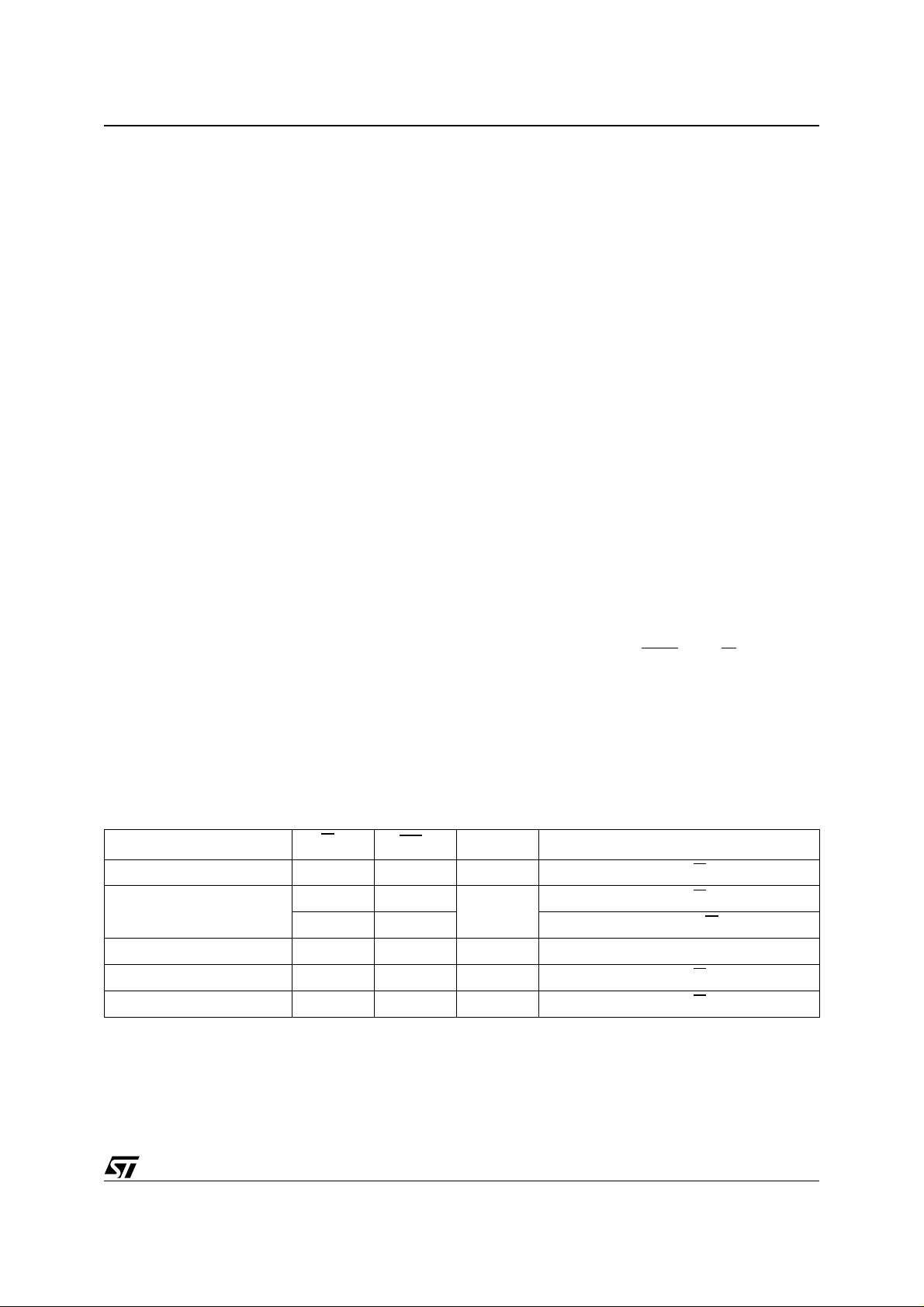
Table 1. Product List
Reference Part Number
128 Kbits
256 Kbits
2
2
C Extended Addressing
C Serial Interface
M24128-BW
M24128-BR
M24256-BW
M24256-BR
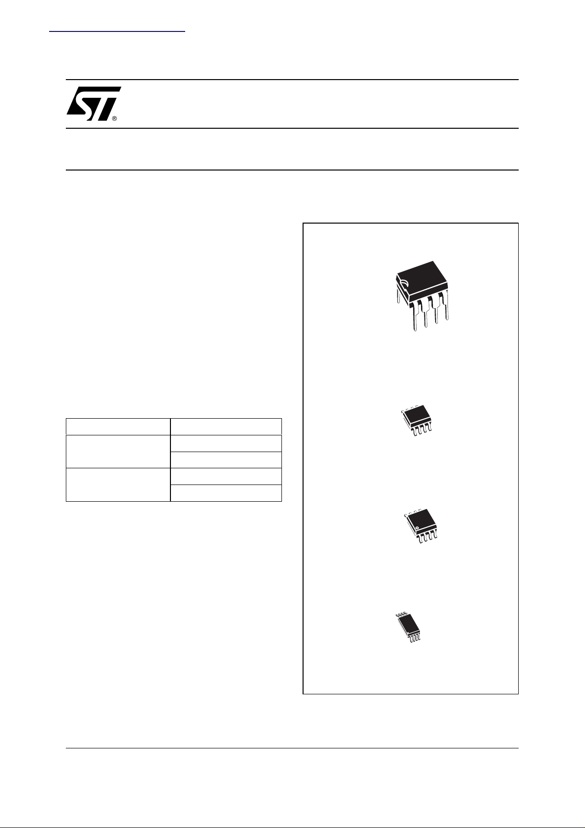
Figure 1. Packages
8
1
PDIP8 (BN)
8
1
SO8 (MN)
150 mil width
8
1
SO8 (MW)
200 mil width
TSSOP8 (DW)
169 mil width
1/25June 2005

M24128-BW, M24128-BR, M24256-BW, M24256-BR
TABLE OF CONTENTS
FEATURES SUMMARY . . . . . . . . . . . . . . . . . . . . . . . . . . . . . . . . . . . . . . . . . . . . . . . . . . . . . . . . . . . . . 1
Table 1. Product List . . . . . . . . . . . . . . . . . . . . . . . . . . . . . . . . . . . . . . . . . . . . . . . . . . . . . . . . . . . . 1
Figure 1. Packages. . . . . . . . . . . . . . . . . . . . . . . . . . . . . . . . . . . . . . . . . . . . . . . . . . . . . . . . . . . . . . 1
Figure 2. Logic Diagram . . . . . . . . . . . . . . . . . . . . . . . . . . . . . . . . . . . . . . . . . . . . . . . . . . . . . . . . . . 4
Table 2. Signal Names . . . . . . . . . . . . . . . . . . . . . . . . . . . . . . . . . . . . . . . . . . . . . . . . . . . . . . . . . . 4
Power On Reset . . . . . . . . . . . . . . . . . . . . . . . . . . . . . . . . . . . . . . . . . . . . . . . . . . . . . . . . . . . . . . . . 4
Figure 3. DIP, SO and TSSOP Connections . . . . . . . . . . . . . . . . . . . . . . . . . . . . . . . . . . . . . . . . . . 4
SIGNAL DESCRIPTION . . . . . . . . . . . . . . . . . . . . . . . . . . . . . . . . . . . . . . . . . . . . . . . . . . . . . . . . . . . . . 5
Serial Clock (SCL). . . . . . . . . . . . . . . . . . . . . . . . . . . . . . . . . . . . . . . . . . . . . . . . . . . . . . . . . . . . . . . 5
Serial Data (SDA) . . . . . . . . . . . . . . . . . . . . . . . . . . . . . . . . . . . . . . . . . . . . . . . . . . . . . . . . . . . . . . . 5
Chip Enable (E0, E1, E2) . . . . . . . . . . . . . . . . . . . . . . . . . . . . . . . . . . . . . . . . . . . . . . . . . . . . . . . . . 5
Write Control (WC) . . . . . . . . . . . . . . . . . . . . . . . . . . . . . . . . . . . . . . . . . . . . . . . . . . . . . . . . . . . . . . 5
Figure 4. Maximum RP Value versus Bus Parasitic Capacitance (C) for an I2C Bus . . . . . . . . . . . 5
Figure 5. I2C Bus Protocol . . . . . . . . . . . . . . . . . . . . . . . . . . . . . . . . . . . . . . . . . . . . . . . . . . . . . . . . 6
Table 3. Device Select Code . . . . . . . . . . . . . . . . . . . . . . . . . . . . . . . . . . . . . . . . . . . . . . . . . . . . . . 6
Table 4. Most Significant Byte . . . . . . . . . . . . . . . . . . . . . . . . . . . . . . . . . . . . . . . . . . . . . . . . . . . . . 6
Table 5. Least Significant Byte . . . . . . . . . . . . . . . . . . . . . . . . . . . . . . . . . . . . . . . . . . . . . . . . . . . . 6
DEVICE OPERATION . . . . . . . . . . . . . . . . . . . . . . . . . . . . . . . . . . . . . . . . . . . . . . . . . . . . . . . . . . . . . . . 7
Start Condition. . . . . . . . . . . . . . . . . . . . . . . . . . . . . . . . . . . . . . . . . . . . . . . . . . . . . . . . . . . . . . . . . 7
Stop Condition. . . . . . . . . . . . . . . . . . . . . . . . . . . . . . . . . . . . . . . . . . . . . . . . . . . . . . . . . . . . . . . . . 7
Acknowledge Bit (ACK) . . . . . . . . . . . . . . . . . . . . . . . . . . . . . . . . . . . . . . . . . . . . . . . . . . . . . . . . . 7
Data Input. . . . . . . . . . . . . . . . . . . . . . . . . . . . . . . . . . . . . . . . . . . . . . . . . . . . . . . . . . . . . . . . . . . . . 7
Memory Addressing . . . . . . . . . . . . . . . . . . . . . . . . . . . . . . . . . . . . . . . . . . . . . . . . . . . . . . . . . . . . 7
Table 6. Operating Modes . . . . . . . . . . . . . . . . . . . . . . . . . . . . . . . . . . . . . . . . . . . . . . . . . . . . . . . . 7
Figure 6. Write Mode Sequences with WC=1 (data write inhibited) . . . . . . . . . . . . . . . . . . . . . . . . . 8
Write Operations . . . . . . . . . . . . . . . . . . . . . . . . . . . . . . . . . . . . . . . . . . . . . . . . . . . . . . . . . . . . . . . 8
Byte Write. . . . . . . . . . . . . . . . . . . . . . . . . . . . . . . . . . . . . . . . . . . . . . . . . . . . . . . . . . . . . . . . . . . . . 8
Page Write . . . . . . . . . . . . . . . . . . . . . . . . . . . . . . . . . . . . . . . . . . . . . . . . . . . . . . . . . . . . . . . . . . . . 9
Figure 7. Write Mode Sequences with WC=0 (data write enabled) . . . . . . . . . . . . . . . . . . . . . . . . . 9
Figure 8. Write Cycle Polling Flowchart using ACK . . . . . . . . . . . . . . . . . . . . . . . . . . . . . . . . . . . . 10
Minimizing System Delays by Polling On ACK. . . . . . . . . . . . . . . . . . . . . . . . . . . . . . . . . . . . . . 10
Figure 9. Read Mode Sequences . . . . . . . . . . . . . . . . . . . . . . . . . . . . . . . . . . . . . . . . . . . . . . . . . . 11
Read Operations . . . . . . . . . . . . . . . . . . . . . . . . . . . . . . . . . . . . . . . . . . . . . . . . . . . . . . . . . . . . . . 11
Random Address Read . . . . . . . . . . . . . . . . . . . . . . . . . . . . . . . . . . . . . . . . . . . . . . . . . . . . . . . . . 11
Current Address Read . . . . . . . . . . . . . . . . . . . . . . . . . . . . . . . . . . . . . . . . . . . . . . . . . . . . . . . . . 11
Sequential Read. . . . . . . . . . . . . . . . . . . . . . . . . . . . . . . . . . . . . . . . . . . . . . . . . . . . . . . . . . . . . . . 12
Acknowledge in Read Mode . . . . . . . . . . . . . . . . . . . . . . . . . . . . . . . . . . . . . . . . . . . . . . . . . . . . .12
INITIAL DELIVERY STATE. . . . . . . . . . . . . . . . . . . . . . . . . . . . . . . . . . . . . . . . . . . . . . . . . . . . . . . . . . 12
MAXIMUM RATING. . . . . . . . . . . . . . . . . . . . . . . . . . . . . . . . . . . . . . . . . . . . . . . . . . . . . . . . . . . . . . . . 13
Table 7. Absolute Maximum Ratings. . . . . . . . . . . . . . . . . . . . . . . . . . . . . . . . . . . . . . . . . . . . . . . 13
2/25

M24128-BW, M24128-BR, M24256-BW, M24256-BR
DC AND AC PARAMETERS. . . . . . . . . . . . . . . . . . . . . . . . . . . . . . . . . . . . . . . . . . . . . . . . . . . . . . . . . 14
Table 8. Operating Conditions (M24128-BW, M24256-BW) . . . . . . . . . . . . . . . . . . . . . . . . . . . . . 14
Table 9. Operating Conditions (M24128-BR, M24256-BR). . . . . . . . . . . . . . . . . . . . . . . . . . . . . . 14
Table 10. AC Measurement Conditions. . . . . . . . . . . . . . . . . . . . . . . . . . . . . . . . . . . . . . . . . . . . . . 14
Figure 10.AC Measurement I/O Waveform . . . . . . . . . . . . . . . . . . . . . . . . . . . . . . . . . . . . . . . . . . . 14
Table 11. Input Parameters. . . . . . . . . . . . . . . . . . . . . . . . . . . . . . . . . . . . . . . . . . . . . . . . . . . . . . . 15
Table 12. DC Characteristics (M24128-BW, M24256-BW) . . . . . . . . . . . . . . . . . . . . . . . . . . . . . . . 15
Table 13. DC Characteristics (M24128-BR, M24256-BR). . . . . . . . . . . . . . . . . . . . . . . . . . . . . . . . 15
Table 14. AC Characteristics ( M24128-BW, M24256-BW). . . . . . . . . . . . . . . . . . . . . . . . . . . . . . . 16
Table 15. AC Characteristics (M24128-BR, M24256-BR) . . . . . . . . . . . . . . . . . . . . . . . . . . . . . . . . 17
Figure 11.AC Waveforms . . . . . . . . . . . . . . . . . . . . . . . . . . . . . . . . . . . . . . . . . . . . . . . . . . . . . . . . 18
PACKAGE MECHANICAL . . . . . . . . . . . . . . . . . . . . . . . . . . . . . . . . . . . . . . . . . . . . . . . . . . . . . . . . . . 19
Figure 12.PDIP8 – 8 pin Plastic DIP, 0.25mm lead frame, Package Outline . . . . . . . . . . . . . . . . . 19
Table 16. PDIP8 – 8 pin Plastic DIP, 0.25mm lead frame, Package Mechanical Data . . . . . . . . . . 19
Figure 13.SO8 narrow – 8 lead Plastic Small Outline, 150 mils body width, Package Outline . . . . 20
Table 17. SO8 narrow – 8 lead Plastic Small Outline, 150 mils body width, Package Mechanical Data
20
Figure 14.SO8 wide – 8 lead Plastic Small Outline, 200 mils body width, Package Outline. . . . . . 21
Table 18. SO8 wide – 8 lead Plastic Small Outline, 200 mils body width, Package Mechanical Data
21
Figure 15.TSSOP8 – 8 lead Thin Shrink Small Outline, Package Outline . . . . . . . . . . . . . . . . . . . 22
Table 19. TSSOP8 – 8 lead Thin Shrink Small Outline, Package Mechanical Data . . . . . . . . . . . . 22
PART NUMBERING . . . . . . . . . . . . . . . . . . . . . . . . . . . . . . . . . . . . . . . . . . . . . . . . . . . . . . . . . . . . . . . 23
Table 20. Ordering Information Scheme . . . . . . . . . . . . . . . . . . . . . . . . . . . . . . . . . . . . . . . . . . . . . 23
REVISION HISTORY. . . . . . . . . . . . . . . . . . . . . . . . . . . . . . . . . . . . . . . . . . . . . . . . . . . . . . . . . . . . . . . 24
Table 21. Document Revision History . . . . . . . . . . . . . . . . . . . . . . . . . . . . . . . . . . . . . . . . . . . . . . . 24
3/25
M24128-BW, M24128-BR, M24256-BW, M24256-BR
SUMMARY DESCRIPTION
These I2C-compatible electrically erasable programmable memory (EEPROM) devices are organized as 32K x 8 bits (M24256-BW and M24256BR) and 16K x 8 bits (M24128-BW and M24128BR).
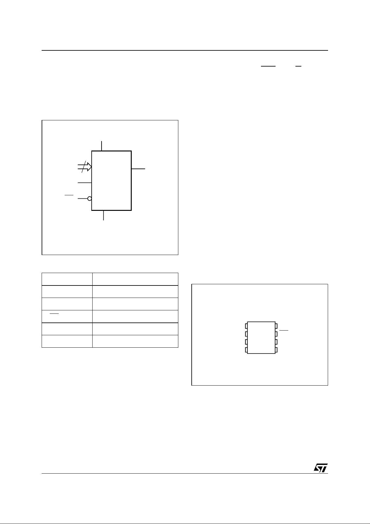
Figure 2. Logic Diagram
V
CC
3
E0-E2
SCL
WC
M24256-B
M24128-B
V
SS
Table 2. Signal Names
SDA
AI02809
ter. The Start condition is followed by a Device
Select Code and Read/Write
bit (RW) (as described in Table 3.), terminated by an acknowledge bit.
When writing data to the memory , the device inserts an acknowled ge bit during the 9
th
bit time,
following the bus master’s 8-bit transmission.
When data is read by the bus master, the bus
master acknowledge s the rec eipt o f the d ata byte
in the same way. Data transfers are terminated by
a Stop condition after an Ack for Write, and after a
NoAck for Read.
Power On Reset
In order to prevent inadvertent Write operations
during Power Up, a Power On Reset (POR) circ uit
is implemented.
At Power Up, the device will not respond to any instruction until V
voltage (this thresho ld i s lo wer tha n th e V
has reached the POR threshold
CC
CC
minimum operating voltage defined in Table 8. and Ta-
ble 9.). In the same wa y, as soon as V
CC
drops
from the normal operating voltage, below the POR
threshold voltage, all th e operations are disabled
and the device will not respond to any instruction.
Prior to selecting and issuing instructions to the
memory, a valid and s table V
voltage must be
CC
applied. This voltage must remain stable and valid
until the end of the transmissi on of the instruc tion
and, for a Write instruction, until the completion of
the internal write cycle (t
).
W
E0, E1, E2 Chip Enable
SDA Serial Data
SCL Serial Clock
WC
V
CC
V
SS
2
C uses a two-wire serial interf ace, comprisi ng a
I
Write Control
Supply Voltage
Ground
bi-directional data line and a clock line. The devices carry a built-in 4-bit Device Type Identifier code
(1010) in accordance with the I
The device behaves as a slave in the I
2
C bus definition.
2
C protocol,
with all memory operations synchronized by the
serial clock. Read and Write operations are initiated by a Start condition, generated by the bus mas-
Figure 3. DIP, SO and TSSOP Connections
M24256-B
M24128-B
E0 V
1
2
E2
3
4
SS
Note: See PACKAGE MECHA NICAL section for package dimen-
sions, and how to identify pin-1.
8
7
6
5
AI02810B
CC
WCE1
SCL
SDAV
4/25
M24128-BW, M24128-BR, M24256-BW, M24256-BR
SIGNAL DESCRIPTION
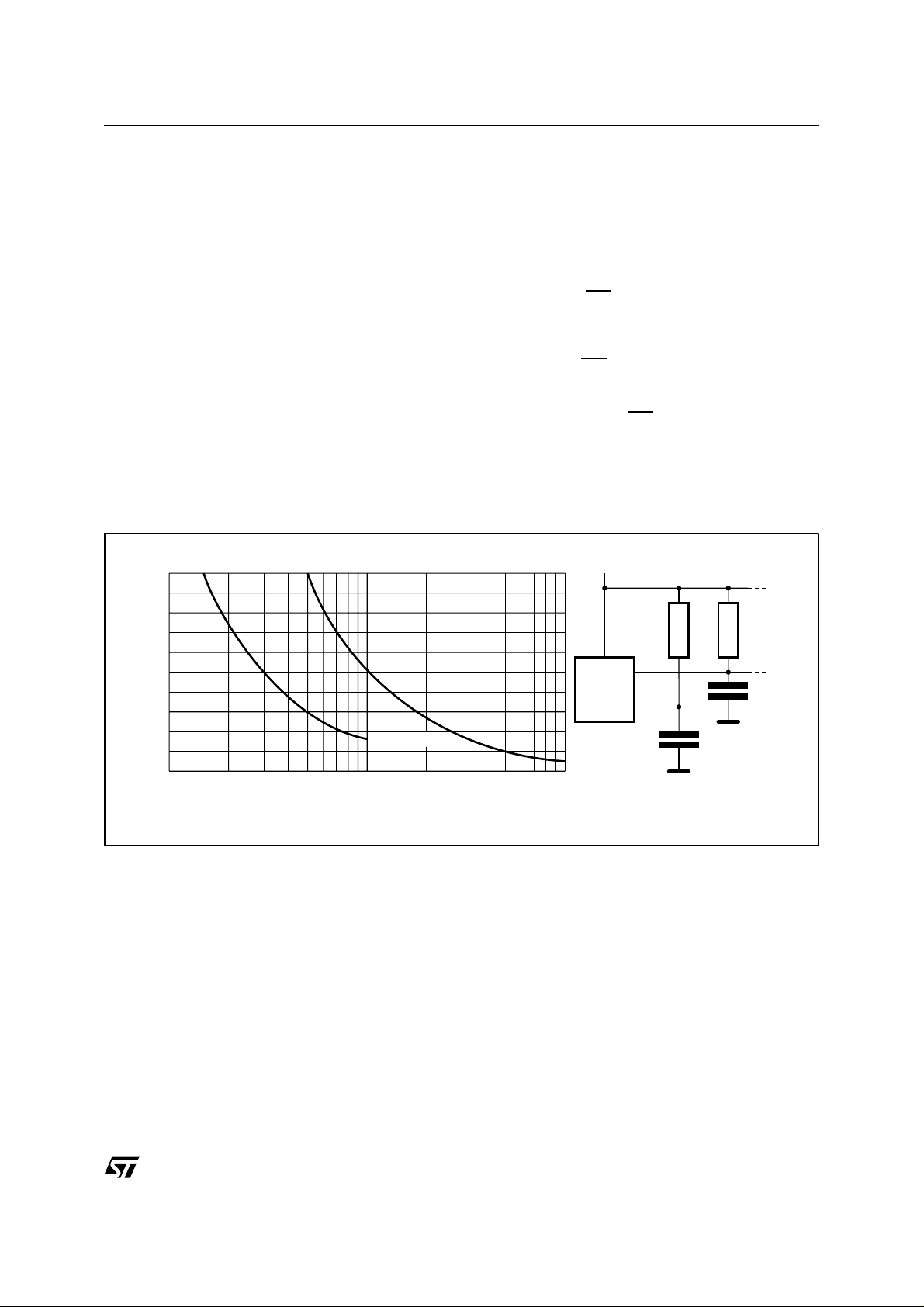
Serial Clock (SCL). This input signal is used to
strobe all data in and out of the device. In applications where this signal is used by slave devices to
synchronize the bus to a slower clock, the bus
master must have an open drain output, and a
pull-up resistor must be connected from Serial
Clock (SCL) to V
value of the pull- up resi stor can be calc ulate d). In
most applications, though, this method of synchronization is not employed, and so the pull-up resistor is not necessary, pro vided that the bus maste r
has a push-pull (rather than open drain) output.
Serial Data (SDA). This bi-directional signal is
used to transfer data in or out of the device. It is an
open drain output that may be wire-OR’ed with
other open drain or ope n collector signals on the
bus. A pull up resistor must be connected from Serial Data (SDA) to V
the value of the pull-up resistor can be calculated).
. (Figure 4. indicates how the
CC
. (Figure 4. indicates how
CC
Chip Enable (E0, E1, E2). These input signals
are used to set the value that is to be looked for on
the three least significant bits (b3, b2, b1) of the 7bit Device Select Code. These inputs must be tied
to V
or VSS, to establish the Device Select
CC
Code. When not connected (left floating), these inputs are read as Low (0,0,0).
Write Control (WC
). This input signal is useful
for protecting the entire content s of the memory
from inadvertent write operations. Write operations are disabled to the entire memory array when
Write Control (WC
nected, the signal is internally read as V
) is driven High. When uncon-
, and
IL
Write operations are allowed.
When Write Contr ol (WC
) is driven High, Device
Select and Address bytes are acknowledged,
Data bytes are not acknowledged.
Figure 4. Maximum R
20
16
12
8
Maximum RP value (kΩ)
4
0
10
Value versus Bus Parasitic Capacitance (C) for an I2C Bus
P
V
CC
SDA
fc = 400kHz
100
C (pF)
fc = 100kHz
MASTER
1000
SCL
R
R
P
P
C
C
AI01665b
5/25
M24128-BW, M24128-BR, M24256-BW, M24256-BR
Figure 5. I2C Bus Protocol
SCL
SDA
SCL
SDA
SCL
SDA
START
Condition
START
Condition
1 23 7 89
MSB
1 23 7 89
MSB
SDA
Input
SDA
Change
STOP
Condition
ACK
ACK
STOP
Condition
AI00792B
Table 3. Device Select Code
Device Type Identifier
1
Chip Enable Address
b7 b6 b5 b4 b3 b2 b1 b0
Device Select Code1010E2E1E0RW
Note: 1. The most significant bit, b7, is sent first.
2. E0, E1 and E2 are compared against the respective ex ternal pins on the memory device.
2
RW
Table 4. Most Significant Byte Table 5. Least Significant Byte
b15 b14 b13 b12 b11 b10 b9 b8 b7 b6 b5 b4 b3 b2 b1 b0
6/25
M24128-BW, M24128-BR, M24256-BW, M24256-BR
DEVICE OPERATION
The device supports the I2C protocol. This is summarized in Figure 5.. Any device that sends d ata
on to the bus is defined to be a transmitter, and
any device that reads the data to be a rec eiver.
The device that controls the data transfer is known
as the bus master, an d th e other a s the s lave device. A data transfer can only be initiated by the
bus master, which will also provide the serial clock
for synchronization. The M24xxx-B device is always a slave in all communication.
Start Condition
Start is identified by a falling edge of Serial Data
(SDA) while Serial Clock (SCL) is stable in the
High state. A Start condition must precede any
data transfer command . The device continuou sly
monitors (except during a Write cycle) Serial Data
(SDA) and Serial Clock (SCL) for a Start condition,
and will not respond unless one is given.
Stop Condition
Stop is identified by a rising edge of Serial Data
(SDA) while Serial Cloc k (S CL) is s tab le a nd d ri ven High. A Stop condition t ermi nate s co mm uni ca tion between the device and the bus master. A
Read command that is follow ed by NoA ck can be
followed by a Sto p condition to force the device
into the Stand-by mode. A S top condition at the
end of a Write comm and trig gers the i nternal EE PROM Write cycle.
Acknowledge Bit (ACK)
The acknowledge bit is used to indicate a successful byte transfer. The bus transmitter, whether it be
bus master or sl ave device, releas es Serial Data
(SDA) after sending ei ght bits of da ta. During the
th
9
clock pulse period, the receiver pulls Serial
Data (SDA) Low to acknowledge the receipt of the
eight data bits.
Data Input
During data input, the device samples Serial Data
(SDA) on the rising edge of Serial Clock (SCL).
For correct device operation, Serial Data (SDA)
must be stable during the rising edge of Serial
Clock (SCL), and the Serial Data (SDA) signal
must change
only
when Serial Cl ock ( SCL ) i s dr iv-
en Low.
Memory Addressing
To start communica tion between the bus master
and the slave device, the b us mas ter m u st ini ti ate
a Start condition. Following this, the bus master
sends the Device Select Code, shown in Table 3.
(on Serial Data (SDA), most significant bit first).
The Device Select Code consists of a 4-bit Device
Type Identifier, and a 3-bit Chip Enable “Address”
(E2, E1, E0). To address the memory array, the 4bit Device Type Identifier is 1010b.
Up to eight memory devices can be connected on
a single I
2
C bus. Each one is gi ven a un ique 3-bit
code on the Chip Enable (E0, E1, E2) inputs.
When the Device Select Code is received, the device only respond s if the Chip Enabl e Address is
the same as the value on the Chip Enable (E0, E1,
E2) inputs.
th
The 8
bit is the Read/Write bit (RW). This bit is
set to 1 for Read and 0 for Write operations.
If a match occurs on the Device Select code, the
corresponding device gives an acknowledgment
on Serial Data (SDA) du ring the 9
th
bit time. If the
device does not match the Devic e Select code, it
deselects itself from the bus, and goes into Standby mode.
Table 6. Operating Modes
Mode RW bit
Current Address Read 1 X 1 START, Device Select, RW
Random Address Read
Sequential Read 1 X ≥ 1 Similar to Current or Random Address Read
Byte Write 0
Page Write 0
Note: 1. X = V
IH
or V
.
IL
0X
1 X reSTART, Device Select, RW
WC
V
V
1
IL
IL
Bytes Initial Sequence
= 1
1
START, Device Select, RW
1 START, Device Select, RW = 0
≤ 64 START, Device Select, RW = 0
= 0, Address
= 1
7/25
M24128-BW, M24128-BR, M24256-BW, M24256-BR
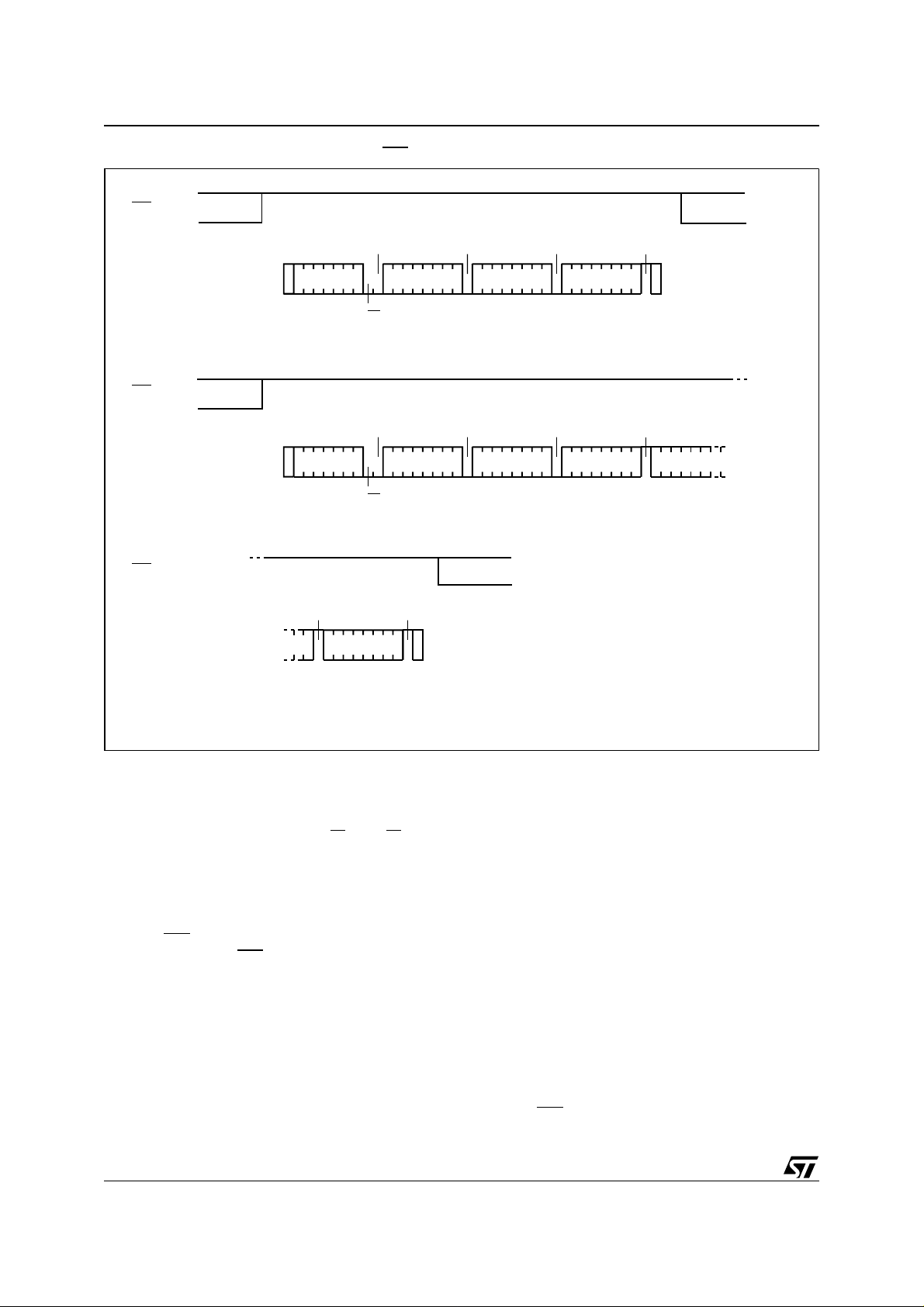
Figure 6. Write Mode Sequences with WC=1 (data write inhibited)
WC
ACK ACK ACK NO ACK
BYTE WRITE DEV SEL BYTE ADDR BYTE ADDR DATA IN
R/W
START
WC
ACK ACK ACK NO ACK
PAGE WRITE DEV SEL BYTE ADDR
R/W
START
WC (cont'd)
NO ACK NO ACK
PAGE WRITE
(cont'd)
DATA IN N
STOP
BYTE ADDR DATA IN 1
STOP
DATA IN 2
AI01120C
Write Operations
Following a Start co ndition the bus mas ter sends
a Device Select Code with the R/W
bit (RW) reset
to 0. The device ack nowledges this , as shown in
Figure 7., and waits for two address bytes. The de-
vice responds to each address byte with an acknowledge bit, and then waits for the data byte.
Writing to the memory may be inhibited if Write
Control (WC
with Write Control (WC
) is driven Hi gh. Any W rite instruction
) driven High (duri ng a pe riod of time from the Start condition until the end of
the two address bytes) will not modify the memory
contents, and the accompanying data bytes are
not
acknowledged, as shown in Figure 6..
Each data byte in the memory ha s a 16-bit (two
byte wide) address. The Most Significant Byte (Ta-
ble 4.) is sent first, foll owed by the Least Signifi-
cant Byte (Table 5.). Bits b15 to b0 form the
address of the byte in memory.
8/25
When the bus master gener ates a Stop conditi on
immediately after t he Ac k bi t (i n th e “1 0
th
bit” time
slot), either at the end of a Byte Write or a Page
Write, the internal memory Write cycle is triggered.
A Stop condition at any othe r time slot does not
trigger the internal Write cycle.
After the Stop condition, the delay t
, and the suc-
W
cessful completion of a Write operation, the device’s internal address counter is incremented
automatically, to point to the next byte address after the last one that was modified.
During the internal Write cycl e, Serial Data (SDA)
is disabled intern ally, a nd the devic e does n ot respond to any requests.
Byte Write
After the Device Select code and the address
bytes, the bus mas ter sends one d ata byte. If the
addressed location is Write-protected, by Write
Control (WC
) being driven High, the device replies

M24128-BW, M24128-BR, M24256-BW, M24256-BR
with NoAck, and the location is not modified. If, instead, the addressed location is not Write-protected, the device replies with Ack. The bus master
terminates the transf er by gener ating a St op condition, as shown in Figure 7..
Page Write
The Page Write mode a llows up to 64 by tes to be
written in a single Wr ite cycle, provided tha t they
are all located in th e same ’row’ in the memory:
that is, the most significant mem ory address bits,
b15-b6, are the same. If more bytes are sent than
will fit up to the end of the row, a condi tion kn own
as ‘roll-over’ occ urs. This should be avoided, as
Figure 7. Write Mode Sequences with WC
WC
BYTE WRITE DEV SEL BYTE ADDR
START
=0 (data write enabled)
ACK
R/W
data star ts t o be com e ov erwr itt en i n a n imp lem entation dependent way.
The bus master sends from 1 to 64 byte s of data,
each of which is acknowledged by the device if
Write Control (WC
) is Low. If Write Control (WC) is
High, the contents of the addressed memory location are not modified, and each data byte is followed by a NoAck. After each byte is transferred,
the internal byte add ress cou nter (th e 6 leas t significant address bits only) is incremented. The
transfer is termina ted by the bus master gener ating a Stop condition.
ACK ACK ACK
BYTE ADDR DATA IN
STOP
WC
ACK ACK ACK ACK
PAGE WRITE DEV SEL BYTE ADDR
R/W
START
WC (cont'd)
ACKACK
PAGE WRITE
(cont'd)
DATA IN N
STOP
BYTE ADDR DATA IN 1
DATA IN 2
AI01106C
9/25

M24128-BW, M24128-BR, M24256-BW, M24256-BR
Figure 8. Write Cycle Polling Flowchart using ACK
WRITE Cycle
in Progress
START Condition
DEVICE SELECT
with RW = 0
ACK
NO
Returned
First byte of instruction
with RW = 0 already
decoded by the device
ReSTART
STOP
YES
Next
Operation is
Addressing the
Memory
DATA for the
WRITE Operation
Continue the
WRITE Operation
Minimizing System Delays by Polling On ACK
During the internal Write cycle, the device disconnects itself from the bus, an d writes a copy of the
data from its internal lat ches to the me mory ce lls.
The maximum Write time (t
) is shown in Table
w
14. and Table 15., but the typical time is shorter.
To make use of this, a polling sequence can be
used by the bus master.
The sequence, as shown in Figure 8., is:
YESNO
Send Address
and Receive ACK
START
Condition
YESNO
DEVICE SELECT
with RW = 1
Continue the
Random READ Operation
AI01847C
– Initial condition: a Write cycle is in progress.
– Step 1: the bus master issues a Start condition
followed by a Device Select Code (the first
byte of the new instruction).
– Step 2: if the device is busy with the internal
Write cycle, no Ack will be returned and the
bus master goes back to Step 1. If the device
has terminated the internal Write cycle, it
responds with an Ack, indicating that the
device is ready to receive the second part of
the instruction (the first byte of this instruction
having been sent during Step 1).
10/25

Figure 9. Read Mode Sequences
M24128-BW, M24128-BR, M24256-BW, M24256-BR
CURRENT
ADDRESS
READ
RANDOM
ADDRESS
READ
SEQUENTIAL
CURRENT
READ
SEQUENTIAL
RANDOM
READ
ACK
DEV SEL DATA OUT
R/W
START
ACK
DEV SEL * BYTE ADDR BYTE ADDR
R/W
START
ACK ACK ACK NO ACK
DEV SEL DATA OUT 1
R/W
START
ACK ACK ACK
DEV SEL * BYTE ADDR BYTE ADDR
NO ACK
STOP
ACK ACK ACK
DEV SEL * DATA OUT
R/W
START
DATA OUT N
STOP
ACK ACK
DEV SEL * DATA OUT 1
NO ACK
STOP
R/W
START
ACK NO ACK
DATA OUT N
STOP
Note: 1. The seven most significant bits of the Device Select Code of a Random Read (in the 1st and 4th bytes) must be identical.
Read Operations
Read operations are per formed independently of
the state of the Write Control (WC
) signal.
After the successful completion of a Read operation, the device’s internal address counter is incremented by one, to point to the next byte address.
Random Address Read
A dummy Write is fi rst performed to load th e address into this addres s counter (as s hown in Fig-
ure 9.) but
without
sending a Stop condition. Then,
the bus master sends another Start condition, and
repeats the Device Select Code, with the RW
bit
set to 1. The devi ce acknowledges thi s, and out-
puts the contents of the addres sed byte. T he bus
master must
nates the transfer with a Stop condition.
Current Address Read
For the Current Address Read operation, following
a Start condition, the bus master only sends a Device Select Code with the R/W
vice acknowledges this, and outputs the byte
addressed by the internal address counter. The
counter is then increment ed. The bus master terminates the transfer with a Stop condition, as
shown in Figure 9.,
byte.
START
not
R/W
AI01105C
acknowledge the byte, and termi-
bit set to 1. The de-
without
acknowledging the
11/25

M24128-BW, M24128-BR, M24256-BW, M24256-BR
Sequential Read
This operation can be used after a Current Address Read or a Random Address Read. The bus
master
and sends additional cloc k pulses so that the device continues to output the next byte in sequence.
To terminate the s tream of by tes, the bu s master
must
generate a Stop condition, as shown in Figure 9..
The output data comes from consecutive addresses, with the internal address counter automatically
incremented after e ach byte outpu t. After the la st
memory address, the addres s cou nter ‘r ol ls- ov er ’,
and the device continues to output data from
memory address 00h.
does
acknowledge the data byte output,
not
acknowledge the last byte, and
must
Acknowledge in Read Mode
For all Read commands, the device waits, after
each byte read, for an acknowledgment during the
th
9
bit time. If the bus master does not drive Serial
Data (SDA) Low during this time, the device terminates the data transfer and switches to its Stand by mode.
INITIAL DELIVERY STATE
The device is deli vered wi th all t he memor y array
bits set to 1 (each byte contains FFh).
12/25

M24128-BW, M24128-BR, M24256-BW, M24256-BR
MAXIMUM RATING
Stressing the devi ce outside the ratings li sted in
Table 7. may cause permanent damage to the de-
vice. These are stress ratings only, and oper ation
of the device at these, or any other conditions outside those indicated in the Oper ating sections of
Table 7. Absolute Maximum Ratings
Symbol Parameter Min. Max. Unit
T
A
T
STG
T
LEAD
V
IO
V
CC
V
ESD
Note: 1. Compliant with JEDEC Std J-STD-020C (for small body, Sn-Pb or Pb assembly), the ST ECOPACK® 7191395 specification, and
the European directive on Restrictions on Hazardous Substances (RoHS) 2002/95/EU
2. AEC-Q100-002 (compliant with JEDEC Std JESD22-A114A, C1=100pF, R1=1500Ω, R2=500Ω)
Ambient Operating Temperature –40 125 °C
Storage Temperature –65 150 °C
Lead Temperature during Soldering
Input or Output range –0.50 6.5 V
Supply Voltage –0.50 6.5 V
Electrostatic Discharge Voltage (Human Body model)
this specificatio n, is not implied. Exposure to Absolute Maximum Rating conditions for extended
periods may affect de vice rel iability. Refer also to
the STMicroelectroni cs SURE Program and othe r
relevant quality documents.
See note
2
–3000 3000 V
1
°C
13/25

M24128-BW, M24128-BR, M24256-BW, M24256-BR
DC AND AC PARAMETERS
This section summ arizes the operati ng and measurement conditions , and the D C an d AC charac teristics of the device. The parameters in th e DC
and AC Characteristic tables that follow are derived from tests performed under the Measure-
Table 8. Operating Conditions (M24128-BW, M24256-BW)
Symbol Parameter Min. Max. Unit
ment Conditions summarized in the relevant
tables. Designers sho uld c heck tha t th e operating
conditions in thei r circui t match the measur ement
conditions when relying on the quoted parameters.
V
CC
T
A
Supply Voltage 2.5 5.5 V
Ambient Operating Temperature –40 85 °C
Table 9. Operating Conditions (M24128-BR, M24256-BR)
Symbol Parameter Min. Max. Unit
V
CC
T
A
Supply Voltage 1.8 5.5 V
Ambient Operating Temperature –40 85 °C
Table 10. AC Measurement Conditions
Symbol Parameter Min. Max. Unit
C
L
Load Capacitance 100 pF
Input Rise and Fall Times 50 ns
0.2V
0.3V
to 0.8V
CC
to 0.7V
CC
CC
CC
Input Levels
Input and Output Timing Referen ce Le ve ls
Figure 10. AC Measurement I/O Waveform
Input Levels
0.8V
CC
0.2V
CC
Input and Output
Timing Reference Levels
0.7V
CC
0.3V
CC
AI00825B
V
V
14/25

M24128-BW, M24128-BR, M24256-BW, M24256-BR
Table 11. Input Parameters
Symbol
C
IN
C
IN
Z
L
Z
H
t
NS
Note: 1. TA = 25°C, f = 400kHz
2. Sampled only, not 100% tested.
Input Capacitance (SDA) 8 pF
Input Capacitance (other pins) 6 pF
Input Impedance (WC)
Pulse width ignored
(Input Filter on SCL and SDA )
Parameter
Table 12. DC Characteristics (M24128-BW, M24256-BW)
Symbol Parameter
Input Leakage Current
I
LI
(SCL, SDA)
I
V
I
I
CC1
V
V
Output Leakage Current
LO
Supply Current
CC
Stand-by Supply Current
Input Low Voltage (SCL, SDA) –0.45
IL
Input High Voltage
IH
(SCL, SDA, WC
Output Low Voltage
OL
1,2
Test Condition Min. Max. Unit
< 0.3 V
V
IN
VIN > 0.7V
CC
CC
Single glitch 100 ns
Test Condition
(in addition to those in Table 8.)
V
= VSS or V
IN
device in Stand-by mode
V
= VSS or V
OUT
=2.5V, fc=400kHz (ri se/ fal l ti me < 3 0ns )
V
CC
= 5V, fc=400kHz (rise/fall time < 30ns)
V
CC
V
= VSS or V
IN
V
= VSS or V
IN
)
I
= 2.1 mA, VCC = 2.5 V
OL
SDA in Hi-Z
CC,
, V
CC
CC
, V
CC
30 kΩ
500 kΩ
Min. Max. Unit
CC
± 2 µA
± 2 µA
1mA
2mA
= 2.5V 2 µA
CC
= 5V
0.7V
CC
10 µA
0.3V
CC
VCC+1 V
0.4 V
V
Table 13. DC Characteristics (M24128-BR, M24 256-BR )
Symbol Parameter
Input Leakage Current
I
LI
(SCL, SDA)
I
I
I
CC1
Output Leakage Current
LO
Supply Current
CC
Stand-by Supply Current
Input Low Voltage (SCL, SDA) –0.45
V
IL
Input Low Voltage
(E2, E1, E0, WC)
V
V
Input High Voltage
IH
(E2, E1, E0, SCL, SDA, WC
Output Low Voltage
OL
(in addition to those in Table 9.)
V
=1.8V, fc=100kHz (rise/fall time < 30ns)
CC
)
Test Condition
V
= VSS or V
IN
device in Stand-by mode
V
= VSS or V
OUT
V
= VSS or V
IN
I
= 0.7 m A, VCC = 1.8 V
OL
SDA in Hi-Z
CC,
, V
CC
CC
CC
= 1.8 V
Min. Max. Unit
± 2 µA
± 2 µA
0.8 mA
1µA
0.3 V
CC
–0.45 0.5 V
CC
VCC+1
0.7V
0.2 V
15/25
V
V

M24128-BW, M24128-BR, M24256-BW, M24256-BR
Table 14. AC Characteristics ( M24128-BW, M24256-BW)
Test conditions specified in Table 8.
Symbol Alt. Parameter Min. Max. Unit
f
C
t
CHCL
t
CLCH
t
CH1CH2
t
CL1CL2
2
t
DH1DH2
2
t
DL1DL2
t
DXCX
t
CLDX
t
CLQX
3
t
CLQV
1
t
CHDX
t
DLCL
t
CHDH
t
DHDL
t
W
Note: 1. For a reSTART condition, or following a Write cycle.
2. Sampled only, not 100% tested.
3. To avoid spurious START and STOP conditions, a minimum delay is placed between SCL=1 and the falling or rising edge of SDA.
f
SCL
t
HIGH
t
LOW
t
R
t
F
t
R
t
F
t
SU:DAT
t
HD:DAT
t
DH
t
AA
t
SU:STA
t
HD:STA
t
SU:STO
t
BUF
t
WR
Clock Frequency 400 kHz
Clock Pulse Width High 600 ns
Clock Pulse Width Low 1300 ns
Clock Rise Time 300 ns
Clock Fall Time 300 ns
SDA Rise Time 20 300 ns
SDA Fall Time 20 300 ns
Data In Set Up Time 100 ns
Data In Hold Time 0 n s
Data Out Hold Time 200 ns
Clock Low to Next Data Valid (Access Time) 200 900 n s
Start Condition Set Up Time 600 ns
Start Condition Hold Time 600 ns
Stop Condition Set Up Time 600 ns
Time between Stop Condition and Next Start
Condition
1300 ns
Write Time 5 ms
16/25

M24128-BW, M24128-BR, M24256-BW, M24256-BR
Table 15. AC Characteristics (M24128-BR, M24 256-BR )
Test conditions specified in Table 9.
Symbol Alt. Parameter Min. Max. Unit
f
C
t
CHCL
t
CLCH
t
CH1CH2
t
CL1CL2
2
t
DH1DH2
2
t
DL1DL2
t
DXCX
t
CLDX
t
CLQX
3
t
CLQV
1
t
CHDX
t
DLCL
t
CHDH
t
DHDL
t
W
Note: 1. For a reSTART condition, or following a Write cycle.
2. Sampled only, not 100% tested.
3. To avoid spurious START and STOP conditions, a minimum delay is placed between SCL=1 and the falling or rising edge of SDA.
f
SCL
t
HIGH
t
LOW
t
R
t
F
t
R
t
F
t
SU:DAT
t
HD:DAT
t
DH
t
AA
t
SU:STA
t
HD:STA
t
SU:STO
t
BUF
t
WR
Clock Frequency 400 kHz
Clock Pulse Width High 600 ns
Clock Pulse Width Low 1300 ns
Clock Rise Time 300 ns
Clock Fall Time 300 ns
SDA Rise Time 20 300 ns
SDA Fall Time 20 300 ns
Data In Set Up Time 100 ns
Data In Hold Time 0 n s
Data Out Hold Time 200 ns
Clock Low to Next Data Valid (Access Time) 200 900 n s
Start Condition Set Up Time 600 ns
Start Condition Hold Time 600 ns
Stop Condition Set Up Time 600 ns
Time between Stop Condition and Next Start
Condition
1300 ns
Write Time 10 ms
17/25

M24128-BW, M24128-BR, M24256-BW, M24256-BR
Figure 11. AC Waveforms
SCL
SDA In
SCL
SDA In
SCL
tCHCL
tDLCL
tCHDX
START
Condition
tCHDH
STOP
Condition
tCLQV tCLQX
SDA
Input
tCLCH
SDA
Change
tW
Write Cycle
tDXCXtCLDX
tCHDH tDHDL
tCHDX
START
Condition
STOP
Condition
START
Condition
SDA Out
Data Valid
AI00795C
18/25

M24128-BW, M24128-BR, M24256-BW, M24256-BR
PACKAGE MECHANICAL
Figure 12. PDIP8 – 8 pin Plastic DIP, 0.25mm lead frame, Package Outline
b2
A2
A1AL
be
D
8
E1
1
Note: Drawing is not to scale.
E
c
eA
eB
PDIP-B
Table 16. PDIP8 – 8 pin Plastic DIP, 0.25mm lead frame, Package Mechanical Data
Symb.
Typ. Min. Max. Typ. Min. Max.
A5.330.210
A1 0.38 0.015
A2 3.30 2.92 4.95 0.130 0.115 0.195
b 0.46 0.36 0.56 0.018 0.014 0.022
b2 1.52 1.14 1.78 0.060 0.045 0.070
c 0.25 0.20 0.36 0.010 0.008 0.014
D 9.27 9.02 10.16 0.365 0.355 0.400
E 7.87 7.62 8.26 0.310 0.300 0.325
E1 6.35 6.10 7.11 0.250 0.240 0.280
e 2.54 – – 0.100 – –
eA 7.62 – – 0.300 – –
eB 10.92 0.430
L 3.30 2.92 3.81 0.130 0.115 0.150
mm inches
19/25

M24128-BW, M24128-BR, M24256-BW, M24256-BR
Figure 13. SO8 narrow – 8 lead Plastic Small Outline, 150 mils body width, Package Outline
h x 45˚
Note: Drawing is not to scale.
B
SO-a
A
e
D
N
1
CP
E
H
C
LA1 α
Table 17. SO8 narrow – 8 lead Plastic Small Outline, 150 mils body width, Package Mechanical Data
Symb.
Typ. Min. Max. Typ. Min. Max.
A 1.35 1.75 0.053 0.069
A1 0.10 0.25 0.004 0.010
B 0.33 0.51 0.013 0.020
C 0.19 0.25 0.007 0.010
D 4.80 5.00 0.189 0.197
E 3.80 4.00 0.150 0.157
e 1.27 – – 0.050 – –
H 5.80 6.20 0.228 0.244
h 0.25 0.50 0.010 0.020
L 0.40 0.90 0.016 0.035
α 0° 8° 0° 8°
N8 8
CP 0.10 0.004
mm inches
20/25

M24128-BW, M24128-BR, M24256-BW, M24256-BR
Figure 14. SO8 wide – 8 lead Plastic Small Outline, 200 mils body width, Package Outline
Note: Drawing is not to scale.
A2
B
e
D
N
1
SO-b
CP
E
H
A
C
LA1 α
Table 18. SO8 wide – 8 lead Plastic Small Outline, 200 mils body width, Package Mechanical Data
Symb.
Typ. Min. Max. Typ. Min. Max.
A2.030.080
A1 0.10 0.25 0.004 0.010
A2 1.78 0.070
B 0.35 0.45 0.014 0.018
C 0.20 – – 0.008 – –
D 5.15 5.35 0.203 0.211
E 5.20 5.40 0.205 0.213
e 1.27 – – 0.050 – –
H 7.70 8.10 0.303 0.319
L 0.50 0.80 0.020 0.031
α 0° 10° 0° 10°
N8 8
CP 0.10 0.004
mm inches
21/25

M24128-BW, M24128-BR, M24256-BW, M24256-BR
Figure 15. TSSOP8 – 8 lead Thin Shrink Small Outline, Package Outline
D
8
1
CP
Note: Drawing is not to scale.
5
EE1
4
α
A2A
A1
eb
L
L1
TSSOP8AM
Table 19. TSSOP8 – 8 lead Thin Shrink Small Outline, Package Mechanical Data
Symbol
Typ. Min. Max. Typ. Min. Max.
A 1.200 0.0472
A1 0.050 0.150 0.0020 0.0059
A2 1.000 0.800 1.050 0.0394 0.0315 0.0413
b 0.190 0.300 0.0075 0.0118
c 0.090 0.200 0.0035 0.0079
CP 0.100 0.0039
D 3.000 2.900 3.100 0.1181 0.1142 0.1220
e 0.650 – – 0.0256 – –
E 6.400 6.200 6.600 0.2520 0.2441 0.2598
E1 4.400 4.300 4.500 0.1732 0.1693 0.1772
L 0.600 0.450 0.750 0.0236 0.0177 0.0295
L1 1.000 0.0394
α 0° 8° 0° 8°
mm inches
c
22/25

M24128-BW, M24128-BR, M24256-BW, M24256-BR
PART NUMBERING
Table 20. Ordering Information Scheme
Example: M24256 – B W MN 6 T P
Device Type
2
M24 = I
Device Function
256 = 256 Kbit (32K x 8)
128 = 128 Kbit (16K x 8)
Operating Voltage
W
R
Package
BN = PDIP8
MN = SO8 (150 mil width)
MW = SO8 (200 mil width)
DW = TSSOP8 (169 mil width)
C serial access EEPROM
3
= VCC = 2.5 to 5.5V
1
= VCC = 1.8 to 5.5V
Device Grade
6 = Industrial temperature range, –40 to 85 °C.
Device tested with standard test flow
Option
blank = Standard Packing
T = Tape and Reel Packing
Plating Technology
blank = Standard SnPb plating
P or G = Lead-Free and RoHS compliant
For a list of available options (speed, package, etc.) or for further information on any aspect of this device,
please contact your nearest ST Sales Office.
23/25

M24128-BW, M24128-BR, M24256-BW, M24256-BR
REVISION HISTORY
Table 21. Document Revision History
Date Rev. Description of Revis io n
28-Dec-1999 2.1 TSSOP8 package added
24-Feb-2000 2.2
22-Nov-2000 2.3 -V voltage range added
30-Jan-2001 2.4
01-Jun-2001 2.5
16-Oct-2001 2.6
09-Nov-2001 2.7 Specification of Test Condition for Leakage Currents in the DC Characteristics table improved
21-Mar-2002 2.8
18-Oct-2002 3.0
20-Nov-2002 3.1
02-Jun-2003 3.2
22-Oct-2003 4.0
16-Apr-2004 5.0
13-Jun-2005 6.0
E2, E1, E0 must be tied to Vcc or Vss
Low Pass Filter Time Constant changed to Glitc h Filte r
-V voltage range changed to 2.5V to 3.6V
Lead Soldering Temperature in the Absolute Maximum Ratings table amended
Write Cycle Polling Flow Chart using ACK illustration updated. SO8(wide) package added
References to PSDIP8 changed to PDIP8, and Package Mechanical data updated
-R voltage range added. Package mechanical data updated for TSSOP8 and TSSOP14
packages according to JEDEC\MO-153
Document promoted from “Preliminary Data” to “Full Data Sheet”
TSSOP14 package removed
Absolute Max Ratings and DC characteristics updated for M24256-BV
1 million Erase/Write cycle endurance for M24256-B and M24256-BW products with process
letter "V"
Document reformatted. Parameters changed are: 1 million Erase/Write cycle endurance and 5
ms write time for M24128-B and M24128-BW products with process letter "B".
Superfluous (and incorrectly present) 100kHz AC Characteristics table for M24256-BR
removed.
Initial delivery state specified. -R and -S ranges are no longer Preliminary Data. Package
mechanical data for unavailable package removed.
Table of contents, and Pb-free options added. Minor wording changes in Summary
Description, Power-On Reset, Memory Addressing, Write Operations, Read Operations.
(min) improved to -0.45V.
V
IL
SO8W package added. Absolute Maximum Ratings for V
(min) and VCC(min) changed.
IO
Soldering temperature information clarified for RoHS compliant devices.
M24xxx-B, M24xxx-BV and M24xxx-BS removed from the datasheet.
Product List summary table added.
Power On Reset paragraph updated.
Figure 4., Maximum RP Value versus Bus Parasitic Capacitance (C) for an I2C Bus updated.
and ZH definition changed.
Z
L
I
CC
and I
updated in Table 12., DC Characteristics (M24128-BW, M24256-BW).
CC1
Device Grade information further clarified to Table 20., Ordering Information Scheme.
24/25

M24128-BW, M24128-BR, M24256-BW, M24256-BR
Information furnished is be lieved to be a ccur ate and reli able. Howe ver, STMicroele ctronic s assu mes no r esponsib ilit y for th e consequences
of use of such information nor for any infrin gement of patent s or other rights of third parties which ma y result from it s use. No license is granted
by implication or otherwi se under any patent or patent rights of STMicroelectronic s. Specifications mentioned in this publication a r e subject
to change without not ice. This pub licat ion su persed es and repl aces all in format ion previou sly su pplie d. STMicroele c tronic s prod ucts ar e no t
authorized for use as critical compone nts in life support devices or systems without express written approval of STMicroelectronics.
The ST logo is a registered trademark of STMicroelectronics.
All other names are the property of their respective owners
© 2005 STMicroelectronics - All rights reserved
Australia - Belgium - Brazil - Canada - China - Czech Republic - Finland - France - Germany - Hong Kong - India - Israel - Italy - Japan -
Malaysia - Malta - Morocco - Singapore - Spain - Sweden - Switzerland - United Kingdom - United States of America
STMicroelectronics group of companies
www.st.com
25/25
 Loading...