

ST LSM320DL User Manual
3D accelerometer sensor and 2D gyroscope sensor
Features
■ Analog supply voltage 2.4 V to 3.6 V
■ Digital supply voltage IOs, 1.8 V
■ Low power mode
■ Power-down mode
■ 3 independent acceleration channels and 2
angular rate channels (pitch and yaw)
■ ±2g/±4g/±8/±16g dynamically selectable full-
scale
■ ±250/±500/±2000 dps dynamically selectable
full-scale
■ Embedded temperature sensor
■ SPI/I
■ Programmable interrupt generator for free-fall
■ ECOPACK
Applications
2
C serial interface (16-bit data output)
and motion detection
®
RoHS and “Green” compliant
LSM320DL
Linear sensor module
Preliminary data
LGA 28L 7.5 x 4.4 x 1.1 mm
The various sensing elements are manufactured
using specialized micromachining processes,
while the IC interfaces are realized using a CMOS
technology that allows to design a dedicated
circuit which is trimmed to better match the
sensing element characteristics.
LSM320DL has a dynamic user selectable fullscale acceleration range of ±2g/±4g/±8/±16g and
angular rate of ±250/±500/±2000 deg/sec.
The accelerometer and gyroscope sensors can
be either activated or put in low power/powerdown mode separately for application optimized
power saving.
■ GPS navigation systems
■ Impact recognition and logging
■ Gaming and virtual reality input devices
■ Motion activated functions
■ Intelligent power saving for handheld devices
■ Vibration monitoring and compensation
■ Free-fall detection
■ 6D orientation detection
Description
The LSM320DL is a system-in-package featuring
a 3D digital accelerometer and a 2D digital
gyroscope.
The LSM320DL is available in a plastic land grid
array (LGA) package.
Several years ago ST successfully pioneered the
use of this package for accelerometers. Today, ST
has the widest manufacturing capability and
strongest expertise in the world for production of
sensors in a plastic LGA package.
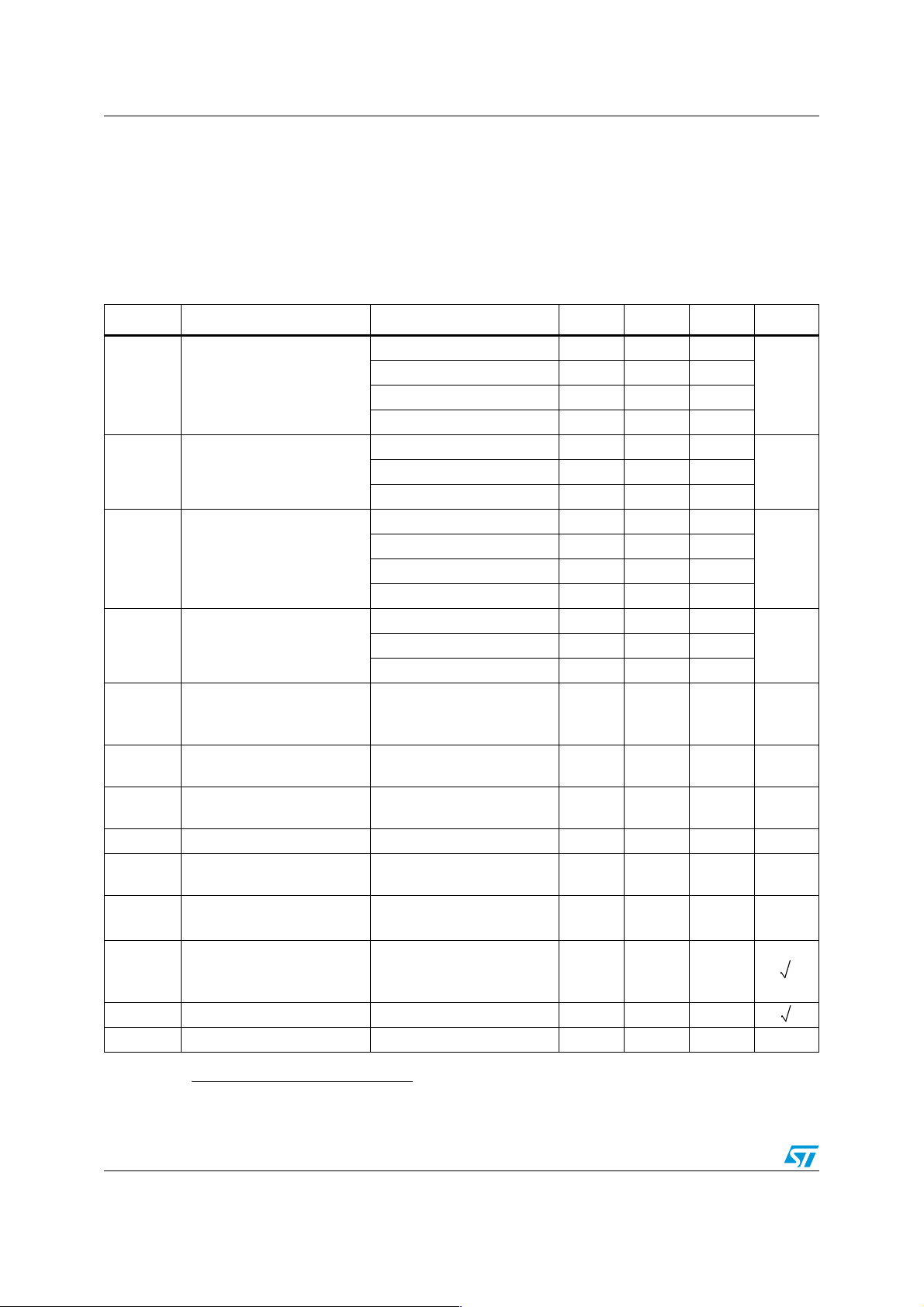
Table 1. Device summary
Order codes
LSM320DL
LSM320DLTR
Temperature
range [°C]
-40 to +85 LGA 28L
Package Packing
Tr ay
Tape and
reel
The ST modules family uses a robust and mature
manufacturing process already used for the
production of micromachined accelerometers.
May 2011 Doc ID 018845 Rev 1 1/53
This is preliminary information on a new product now in development or undergoing evaluation. Details are subject to
change without notice.
www.st.com
53

Contents LSM320DL
Contents
1 Block diagram and pin description . . . . . . . . . . . . . . . . . . . . . . . . . . . . . 9
1.1 Block diagram . . . . . . . . . . . . . . . . . . . . . . . . . . . . . . . . . . . . . . . . . . . . . . . 9
1.2 Pin description . . . . . . . . . . . . . . . . . . . . . . . . . . . . . . . . . . . . . . . . . . . . . 10
2 Module specifications . . . . . . . . . . . . . . . . . . . . . . . . . . . . . . . . . . . . . . . 12
2.1 Mechanical characteristics . . . . . . . . . . . . . . . . . . . . . . . . . . . . . . . . . . . . 12
2.2 Electrical characteristics . . . . . . . . . . . . . . . . . . . . . . . . . . . . . . . . . . . . . . 13
2.3 Temperature sensor characteristics . . . . . . . . . . . . . . . . . . . . . . . . . . . . . 14
2.4 Communication interface characteristics . . . . . . . . . . . . . . . . . . . . . . . . . 15
2.4.1 SPI - serial peripheral interface . . . . . . . . . . . . . . . . . . . . . . . . . . . . . . . 15
2.4.2 I2C - inter IC control interface . . . . . . . . . . . . . . . . . . . . . . . . . . . . . . . . 16
2.5 Absolute maximum ratings . . . . . . . . . . . . . . . . . . . . . . . . . . . . . . . . . . . . 17
2.6 Terminology . . . . . . . . . . . . . . . . . . . . . . . . . . . . . . . . . . . . . . . . . . . . . . . 18
2.6.1 Sensitivity . . . . . . . . . . . . . . . . . . . . . . . . . . . . . . . . . . . . . . . . . . . . . . . . 18
2.6.2 Zero level . . . . . . . . . . . . . . . . . . . . . . . . . . . . . . . . . . . . . . . . . . . . . . . . 18
3 Functionality . . . . . . . . . . . . . . . . . . . . . . . . . . . . . . . . . . . . . . . . . . . . . . 19
3.1 Factory calibration . . . . . . . . . . . . . . . . . . . . . . . . . . . . . . . . . . . . . . . . . . 19
4 Application hints . . . . . . . . . . . . . . . . . . . . . . . . . . . . . . . . . . . . . . . . . . . 20
4.1 External capacitors . . . . . . . . . . . . . . . . . . . . . . . . . . . . . . . . . . . . . . . . . . 20
4.2 Soldering information . . . . . . . . . . . . . . . . . . . . . . . . . . . . . . . . . . . . . . . . 21
5 Digital interfaces . . . . . . . . . . . . . . . . . . . . . . . . . . . . . . . . . . . . . . . . . . . 22
5.1 I2C serial interface . . . . . . . . . . . . . . . . . . . . . . . . . . . . . . . . . . . . . . . . . . 22
5.1.1 I2C operation . . . . . . . . . . . . . . . . . . . . . . . . . . . . . . . . . . . . . . . . . . . . . 23
5.2 SPI bus interface . . . . . . . . . . . . . . . . . . . . . . . . . . . . . . . . . . . . . . . . . . . 25
5.2.1 SPI read . . . . . . . . . . . . . . . . . . . . . . . . . . . . . . . . . . . . . . . . . . . . . . . . . 26
5.2.2 SPI write . . . . . . . . . . . . . . . . . . . . . . . . . . . . . . . . . . . . . . . . . . . . . . . . 26
5.2.3 SPI read in 3-wire mode . . . . . . . . . . . . . . . . . . . . . . . . . . . . . . . . . . . . 27
6 Register mapping . . . . . . . . . . . . . . . . . . . . . . . . . . . . . . . . . . . . . . . . . . 28
2/53 Doc ID 018845 Rev 1

LSM320DL Contents
7 Registers description . . . . . . . . . . . . . . . . . . . . . . . . . . . . . . . . . . . . . . . 30
7.1 CTRL_REG1_A (20h) . . . . . . . . . . . . . . . . . . . . . . . . . . . . . . . . . . . . . . . 30
7.2 CTRL_REG2_A (21h) . . . . . . . . . . . . . . . . . . . . . . . . . . . . . . . . . . . . . . . 31
7.3 CTRL_REG3_A (22h) . . . . . . . . . . . . . . . . . . . . . . . . . . . . . . . . . . . . . . . 31
7.4 CTRL_REG4_A (23h) . . . . . . . . . . . . . . . . . . . . . . . . . . . . . . . . . . . . . . . 32
7.5 CTRL_REG5_A (24h) . . . . . . . . . . . . . . . . . . . . . . . . . . . . . . . . . . . . . . . 32
7.6 CTRL_REG6_A (25h) . . . . . . . . . . . . . . . . . . . . . . . . . . . . . . . . . . . . . . . 33
7.7 REFERENCE/DATACAPTURE_A (26h) . . . . . . . . . . . . . . . . . . . . . . . . . . 33
7.8 STATUS_REG_A (27h) . . . . . . . . . . . . . . . . . . . . . . . . . . . . . . . . . . . . . . 33
7.9 OUT_X_L_A (28h), OUT_X_H_A (29h) . . . . . . . . . . . . . . . . . . . . . . . . . . 34
7.10 OUT_Y_L_A (2Ah), OUT_Y_H_A (2Bh) . . . . . . . . . . . . . . . . . . . . . . . . . 34
7.11 OUT_Z_L _A(2Ch), OUT_Z_H_A (2Dh) . . . . . . . . . . . . . . . . . . . . . . . . . 34
7.12 FIFO_CTRL_REG_A (2Eh) . . . . . . . . . . . . . . . . . . . . . . . . . . . . . . . . . . . 34
7.13 FIFO_SRC_REG_A (2Fh) . . . . . . . . . . . . . . . . . . . . . . . . . . . . . . . . . . . . 35
7.14 INT1_CFG_A (30h) . . . . . . . . . . . . . . . . . . . . . . . . . . . . . . . . . . . . . . . . . 35
7.15 INT1_SRC_A (31h) . . . . . . . . . . . . . . . . . . . . . . . . . . . . . . . . . . . . . . . . . 36
7.16 INT1_THS_A (32h) . . . . . . . . . . . . . . . . . . . . . . . . . . . . . . . . . . . . . . . . . . 36
7.17 INT1_DURATION_A (33h) . . . . . . . . . . . . . . . . . . . . . . . . . . . . . . . . . . . . 37
7.18 CLICK_CFG _A (38h) . . . . . . . . . . . . . . . . . . . . . . . . . . . . . . . . . . . . . . . 37
7.19 CLICK_SRC_A (39h) . . . . . . . . . . . . . . . . . . . . . . . . . . . . . . . . . . . . . . . . 37
7.20 CLICK_THS_A (3Ah) . . . . . . . . . . . . . . . . . . . . . . . . . . . . . . . . . . . . . . . . 38
7.21 TIME_LIMIT_A (3Bh) . . . . . . . . . . . . . . . . . . . . . . . . . . . . . . . . . . . . . . . . 38
7.22 TIME_LATENCY_A (3Ch) . . . . . . . . . . . . . . . . . . . . . . . . . . . . . . . . . . . . 38
7.23 TIME WINDOW_A (3Dh) . . . . . . . . . . . . . . . . . . . . . . . . . . . . . . . . . . . . . 39
7.24 CTRL_REG1_G (20h) . . . . . . . . . . . . . . . . . . . . . . . . . . . . . . . . . . . . . . . 39
7.25 CTRL_REG2_G (21h) . . . . . . . . . . . . . . . . . . . . . . . . . . . . . . . . . . . . . . . 40
7.26 CTRL_REG3_G (22h) . . . . . . . . . . . . . . . . . . . . . . . . . . . . . . . . . . . . . . . 41
7.27 CTRL_REG4_G (23h) . . . . . . . . . . . . . . . . . . . . . . . . . . . . . . . . . . . . . . . 42
7.28 CTRL_REG5_G (24h) . . . . . . . . . . . . . . . . . . . . . . . . . . . . . . . . . . . . . . . 42
7.29 REFERENCE/DATACAPTURE_G (25h) . . . . . . . . . . . . . . . . . . . . . . . . . 44
7.30 OUT_TEMP_G (26h) . . . . . . . . . . . . . . . . . . . . . . . . . . . . . . . . . . . . . . . . 44
7.31 STATUS_REG_G (27h) . . . . . . . . . . . . . . . . . . . . . . . . . . . . . . . . . . . . . . 44
7.32 OUT_X_L_G (28h), OUT_X_H_G (29h) . . . . . . . . . . . . . . . . . . . . . . . . . 45
Doc ID 018845 Rev 1 3/53

Contents LSM320DL
7.33 OUT_Z_L_G (2Ch), OUT_Z_H_G (2Dh) . . . . . . . . . . . . . . . . . . . . . . . . . 45
7.34 FIFO_CTRL_REG_G (2Eh) . . . . . . . . . . . . . . . . . . . . . . . . . . . . . . . . . . . 45
7.35 FIFO_SRC_REG_G (2Fh) . . . . . . . . . . . . . . . . . . . . . . . . . . . . . . . . . . . . 45
7.36 INT1_CFG_G (30h) . . . . . . . . . . . . . . . . . . . . . . . . . . . . . . . . . . . . . . . . . 46
7.37 INT1_SRC_G (31h) . . . . . . . . . . . . . . . . . . . . . . . . . . . . . . . . . . . . . . . . . 46
7.38 INT1_THS_XH_G (32h) . . . . . . . . . . . . . . . . . . . . . . . . . . . . . . . . . . . . . . 47
7.39 INT1_THS_XL_G (33h) . . . . . . . . . . . . . . . . . . . . . . . . . . . . . . . . . . . . . . 47
7.40 INT1_THS_ZH_G (36h) . . . . . . . . . . . . . . . . . . . . . . . . . . . . . . . . . . . . . . 47
7.41 INT1_THS_ZL_G (37h) . . . . . . . . . . . . . . . . . . . . . . . . . . . . . . . . . . . . . . 48
7.42 INT1_DURATION_G (38h) . . . . . . . . . . . . . . . . . . . . . . . . . . . . . . . . . . . . 48
8 Package information . . . . . . . . . . . . . . . . . . . . . . . . . . . . . . . . . . . . . . . . 50
9 Revision history . . . . . . . . . . . . . . . . . . . . . . . . . . . . . . . . . . . . . . . . . . . 52
4/53 Doc ID 018845 Rev 1

LSM320DL List of tables
List of tables
Table 1. Device summary . . . . . . . . . . . . . . . . . . . . . . . . . . . . . . . . . . . . . . . . . . . . . . . . . . . . . . . . . . 1
Table 2. Pin description . . . . . . . . . . . . . . . . . . . . . . . . . . . . . . . . . . . . . . . . . . . . . . . . . . . . . . . . . . 10
Table 3. Mechanical characteristics . . . . . . . . . . . . . . . . . . . . . . . . . . . . . . . . . . . . . . . . . . . . . . . . . 12
Table 4. Electrical characteristics . . . . . . . . . . . . . . . . . . . . . . . . . . . . . . . . . . . . . . . . . . . . . . . . . . . 13
Table 5. Temperature sensor characteristics . . . . . . . . . . . . . . . . . . . . . . . . . . . . . . . . . . . . . . . . . . 14
Table 6. SPI slave timing values. . . . . . . . . . . . . . . . . . . . . . . . . . . . . . . . . . . . . . . . . . . . . . . . . . . . 15
Table 7. I2C slave timing values . . . . . . . . . . . . . . . . . . . . . . . . . . . . . . . . . . . . . . . . . . . . . . . . . . . . 16
Table 8. Absolute maximum ratings . . . . . . . . . . . . . . . . . . . . . . . . . . . . . . . . . . . . . . . . . . . . . . . . . 17
Table 9. Part list . . . . . . . . . . . . . . . . . . . . . . . . . . . . . . . . . . . . . . . . . . . . . . . . . . . . . . . . . . . . . . . . 20
Table 10. Serial interface pin description . . . . . . . . . . . . . . . . . . . . . . . . . . . . . . . . . . . . . . . . . . . . . . 22
Table 11. Serial interface pin description . . . . . . . . . . . . . . . . . . . . . . . . . . . . . . . . . . . . . . . . . . . . . . 22
Table 12. Transfer when master is writing one byte to slave . . . . . . . . . . . . . . . . . . . . . . . . . . . . . . . 23
Table 13. Transfer when master is writing multiple bytes to slave:. . . . . . . . . . . . . . . . . . . . . . . . . . . 23
Table 14. Transfer when master is receiving (reading) one byte of data from slave: . . . . . . . . . . . . . 23
Table 15. Transfer when master is receiving (reading) multiple bytes of data from slave . . . . . . . . . 23
Table 16. Linear acceleration SAD+Read/Write patterns . . . . . . . . . . . . . . . . . . . . . . . . . . . . . . . . . . 24
Table 17. Angular rate SAD+Read/Write patterns . . . . . . . . . . . . . . . . . . . . . . . . . . . . . . . . . . . . . . . 24
Table 18. Register address map. . . . . . . . . . . . . . . . . . . . . . . . . . . . . . . . . . . . . . . . . . . . . . . . . . . . . 28
Table 19. CTRL_REG1_A register . . . . . . . . . . . . . . . . . . . . . . . . . . . . . . . . . . . . . . . . . . . . . . . . . . . 30
Table 20. CTRL_REG1_A description . . . . . . . . . . . . . . . . . . . . . . . . . . . . . . . . . . . . . . . . . . . . . . . . 30
Table 21. Data rate configuration . . . . . . . . . . . . . . . . . . . . . . . . . . . . . . . . . . . . . . . . . . . . . . . . . . . . 30
Table 22. CTRL_REG2_A register . . . . . . . . . . . . . . . . . . . . . . . . . . . . . . . . . . . . . . . . . . . . . . . . . . . 31
Table 23. CTRL_REG2_A description . . . . . . . . . . . . . . . . . . . . . . . . . . . . . . . . . . . . . . . . . . . . . . . . 31
Table 24. High pass filter mode configuration . . . . . . . . . . . . . . . . . . . . . . . . . . . . . . . . . . . . . . . . . . 31
Table 25. CTRL_REG3_A register . . . . . . . . . . . . . . . . . . . . . . . . . . . . . . . . . . . . . . . . . . . . . . . . . . . 31
Table 26. CTRL_REG3_A description . . . . . . . . . . . . . . . . . . . . . . . . . . . . . . . . . . . . . . . . . . . . . . . . 31
Table 27. CTRL_REG4_A register . . . . . . . . . . . . . . . . . . . . . . . . . . . . . . . . . . . . . . . . . . . . . . . . . . . 32
Table 28. CTRL_REG4_A description . . . . . . . . . . . . . . . . . . . . . . . . . . . . . . . . . . . . . . . . . . . . . . . . 32
Table 29. CTRL_REG5_A register . . . . . . . . . . . . . . . . . . . . . . . . . . . . . . . . . . . . . . . . . . . . . . . . . . . 32
Table 30. CTRL_REG5_A description . . . . . . . . . . . . . . . . . . . . . . . . . . . . . . . . . . . . . . . . . . . . . . . . 32
Table 31. CTRL_REG6_A register . . . . . . . . . . . . . . . . . . . . . . . . . . . . . . . . . . . . . . . . . . . . . . . . . . . 33
Table 32. CTRL_REG6 description . . . . . . . . . . . . . . . . . . . . . . . . . . . . . . . . . . . . . . . . . . . . . . . . . . 33
Table 33. REFERENCE_A register . . . . . . . . . . . . . . . . . . . . . . . . . . . . . . . . . . . . . . . . . . . . . . . . . . 33
Table 34. REFERENCE register description . . . . . . . . . . . . . . . . . . . . . . . . . . . . . . . . . . . . . . . . . . . 33
Table 35. STATUS_REG_A register . . . . . . . . . . . . . . . . . . . . . . . . . . . . . . . . . . . . . . . . . . . . . . . . . 33
Table 36. STATUS_REG_A register description . . . . . . . . . . . . . . . . . . . . . . . . . . . . . . . . . . . . . . . . 33
Table 37. FIFO_CTRL_REG_A register . . . . . . . . . . . . . . . . . . . . . . . . . . . . . . . . . . . . . . . . . . . . . . . 34
Table 38. FIFO_CTRL_REG_A register description. . . . . . . . . . . . . . . . . . . . . . . . . . . . . . . . . . . . . . 34
Table 39. FIFO mode configuration . . . . . . . . . . . . . . . . . . . . . . . . . . . . . . . . . . . . . . . . . . . . . . . . . . 34
Table 40. FIFO_SRC_REG_A register . . . . . . . . . . . . . . . . . . . . . . . . . . . . . . . . . . . . . . . . . . . . . . . . 35
Table 41. INT1_CFG_REG_A register . . . . . . . . . . . . . . . . . . . . . . . . . . . . . . . . . . . . . . . . . . . . . . . . 35
Table 42. INT1_CFG_REG_A description . . . . . . . . . . . . . . . . . . . . . . . . . . . . . . . . . . . . . . . . . . . . . 35
Table 43. Interrupt mode . . . . . . . . . . . . . . . . . . . . . . . . . . . . . . . . . . . . . . . . . . . . . . . . . . . . . . . . . . 35
Table 44. INT1_SRC_A register . . . . . . . . . . . . . . . . . . . . . . . . . . . . . . . . . . . . . . . . . . . . . . . . . . . . . 36
Table 45. INT1_SRC_A description . . . . . . . . . . . . . . . . . . . . . . . . . . . . . . . . . . . . . . . . . . . . . . . . . . 36
Table 46. INT1_THS_A register . . . . . . . . . . . . . . . . . . . . . . . . . . . . . . . . . . . . . . . . . . . . . . . . . . . . . 36
Table 47. INT1_THS_A description . . . . . . . . . . . . . . . . . . . . . . . . . . . . . . . . . . . . . . . . . . . . . . . . . . 36
Table 48. INT1_DURATION_Aregister . . . . . . . . . . . . . . . . . . . . . . . . . . . . . . . . . . . . . . . . . . . . . . . . 37
Doc ID 018845 Rev 1 5/53

List of tables LSM320DL
Table 49. INT1_DURATION_A description . . . . . . . . . . . . . . . . . . . . . . . . . . . . . . . . . . . . . . . . . . . . 37
Table 50. CLICK_CFG_A register . . . . . . . . . . . . . . . . . . . . . . . . . . . . . . . . . . . . . . . . . . . . . . . . . . . 37
Table 51. CLICK_CFG_A description . . . . . . . . . . . . . . . . . . . . . . . . . . . . . . . . . . . . . . . . . . . . . . . . . 37
Table 52. CLICK_SRC_A register . . . . . . . . . . . . . . . . . . . . . . . . . . . . . . . . . . . . . . . . . . . . . . . . . . . 37
Table 53. CLICK_SRC_A description . . . . . . . . . . . . . . . . . . . . . . . . . . . . . . . . . . . . . . . . . . . . . . . . . 38
Table 54. CLICK_THS_A register. . . . . . . . . . . . . . . . . . . . . . . . . . . . . . . . . . . . . . . . . . . . . . . . . . . . 38
Table 55. CLICK_SRC_A description . . . . . . . . . . . . . . . . . . . . . . . . . . . . . . . . . . . . . . . . . . . . . . . . . 38
Table 56. TIME_LIMIT_A register. . . . . . . . . . . . . . . . . . . . . . . . . . . . . . . . . . . . . . . . . . . . . . . . . . . . 38
Table 57. TIME_LIMIT_A description . . . . . . . . . . . . . . . . . . . . . . . . . . . . . . . . . . . . . . . . . . . . . . . . . 38
Table 58. TIME_LATENCY_A register . . . . . . . . . . . . . . . . . . . . . . . . . . . . . . . . . . . . . . . . . . . . . . . . 38
Table 59. TIME_LATENCY_A description . . . . . . . . . . . . . . . . . . . . . . . . . . . . . . . . . . . . . . . . . . . . . 39
Table 60. TIME_WINDOW_A register . . . . . . . . . . . . . . . . . . . . . . . . . . . . . . . . . . . . . . . . . . . . . . . . 39
Table 61. TIME_WINDOW_A description. . . . . . . . . . . . . . . . . . . . . . . . . . . . . . . . . . . . . . . . . . . . . . 39
Table 62. CTRL_REG1_G register . . . . . . . . . . . . . . . . . . . . . . . . . . . . . . . . . . . . . . . . . . . . . . . . . . . 39
Table 63. CTRL_REG1_G description . . . . . . . . . . . . . . . . . . . . . . . . . . . . . . . . . . . . . . . . . . . . . . . . 39
Table 64. DR and BW configuration setting . . . . . . . . . . . . . . . . . . . . . . . . . . . . . . . . . . . . . . . . . . . . 40
Table 65. Power mode selection configuration . . . . . . . . . . . . . . . . . . . . . . . . . . . . . . . . . . . . . . . . . . 40
Table 66. CTRL_REG2_G register . . . . . . . . . . . . . . . . . . . . . . . . . . . . . . . . . . . . . . . . . . . . . . . . . . . 40
Table 67. CTRL_REG2_G description . . . . . . . . . . . . . . . . . . . . . . . . . . . . . . . . . . . . . . . . . . . . . . . . 41
Table 68. High pass filter mode configuration . . . . . . . . . . . . . . . . . . . . . . . . . . . . . . . . . . . . . . . . . . 41
Table 69. High pass filter cut-off frequency configuration [Hz] . . . . . . . . . . . . . . . . . . . . . . . . . . . . . . 41
Table 70. CTRL_REG1_G register . . . . . . . . . . . . . . . . . . . . . . . . . . . . . . . . . . . . . . . . . . . . . . . . . . . 41
Table 71. CTRL_REG3_G description . . . . . . . . . . . . . . . . . . . . . . . . . . . . . . . . . . . . . . . . . . . . . . . . 41
Table 72. CTRL_REG4_G register . . . . . . . . . . . . . . . . . . . . . . . . . . . . . . . . . . . . . . . . . . . . . . . . . . . 42
Table 73. CTRL_REG4_G description . . . . . . . . . . . . . . . . . . . . . . . . . . . . . . . . . . . . . . . . . . . . . . . . 42
Table 74. CTRL_REG5_G register . . . . . . . . . . . . . . . . . . . . . . . . . . . . . . . . . . . . . . . . . . . . . . . . . . . 42
Table 75. CTRL_REG5_G description . . . . . . . . . . . . . . . . . . . . . . . . . . . . . . . . . . . . . . . . . . . . . . . . 42
Table 76. Out_Sel configuration setting . . . . . . . . . . . . . . . . . . . . . . . . . . . . . . . . . . . . . . . . . . . . . . . 43
Table 77. INT_SEL configuration setting . . . . . . . . . . . . . . . . . . . . . . . . . . . . . . . . . . . . . . . . . . . . . . 43
Table 78. REFERENCE_G register . . . . . . . . . . . . . . . . . . . . . . . . . . . . . . . . . . . . . . . . . . . . . . . . . . 44
Table 79. REFERENCE_G register description . . . . . . . . . . . . . . . . . . . . . . . . . . . . . . . . . . . . . . . . . 44
Table 80. OUT_TEMP_G register . . . . . . . . . . . . . . . . . . . . . . . . . . . . . . . . . . . . . . . . . . . . . . . . . . . 44
Table 81. OUT_TEMP_G register description . . . . . . . . . . . . . . . . . . . . . . . . . . . . . . . . . . . . . . . . . . 44
Table 82. STATUS_REG_G register . . . . . . . . . . . . . . . . . . . . . . . . . . . . . . . . . . . . . . . . . . . . . . . . . 44
Table 83. STATUS_REG_G description. . . . . . . . . . . . . . . . . . . . . . . . . . . . . . . . . . . . . . . . . . . . . . . 44
Table 84. REFERENCE_G register . . . . . . . . . . . . . . . . . . . . . . . . . . . . . . . . . . . . . . . . . . . . . . . . . . 45
Table 85. REFERENCE_G register description . . . . . . . . . . . . . . . . . . . . . . . . . . . . . . . . . . . . . . . . . 45
Table 86. FIFO mode configuration . . . . . . . . . . . . . . . . . . . . . . . . . . . . . . . . . . . . . . . . . . . . . . . . . . 45
Table 87. FIFO_SRC_G register . . . . . . . . . . . . . . . . . . . . . . . . . . . . . . . . . . . . . . . . . . . . . . . . . . . . 45
Table 88. FIFO_SRC_G register description . . . . . . . . . . . . . . . . . . . . . . . . . . . . . . . . . . . . . . . . . . . 46
Table 89. INT1_CFG_G register. . . . . . . . . . . . . . . . . . . . . . . . . . . . . . . . . . . . . . . . . . . . . . . . . . . . . 46
Table 90. INT1_CFG_G description . . . . . . . . . . . . . . . . . . . . . . . . . . . . . . . . . . . . . . . . . . . . . . . . . . 46
Table 91. INT1_SRC_G register. . . . . . . . . . . . . . . . . . . . . . . . . . . . . . . . . . . . . . . . . . . . . . . . . . . . . 46
Table 92. INT1_SRC_G description . . . . . . . . . . . . . . . . . . . . . . . . . . . . . . . . . . . . . . . . . . . . . . . . . . 47
Table 93. INT1_THS_XH_G register . . . . . . . . . . . . . . . . . . . . . . . . . . . . . . . . . . . . . . . . . . . . . . . . . 47
Table 94. INT1_THS_XH_G description. . . . . . . . . . . . . . . . . . . . . . . . . . . . . . . . . . . . . . . . . . . . . . . 47
Table 95. INT1_THS_XL_G register. . . . . . . . . . . . . . . . . . . . . . . . . . . . . . . . . . . . . . . . . . . . . . . . . . 47
Table 96. INT1_THS_XL_G description . . . . . . . . . . . . . . . . . . . . . . . . . . . . . . . . . . . . . . . . . . . . . . . 47
Table 97. INT1_THS_ZH_G register . . . . . . . . . . . . . . . . . . . . . . . . . . . . . . . . . . . . . . . . . . . . . . . . . 47
Table 98. INT1_THS_ZH_G description . . . . . . . . . . . . . . . . . . . . . . . . . . . . . . . . . . . . . . . . . . . . . . . 48
Table 99. INT1_THS_ZL_G register . . . . . . . . . . . . . . . . . . . . . . . . . . . . . . . . . . . . . . . . . . . . . . . . . . 48
6/53 Doc ID 018845 Rev 1

LSM320DL List of tables
Table 100. INT1_THS_ZL_G description . . . . . . . . . . . . . . . . . . . . . . . . . . . . . . . . . . . . . . . . . . . . . . . 48
Table 101. INT1_DURATION_G register . . . . . . . . . . . . . . . . . . . . . . . . . . . . . . . . . . . . . . . . . . . . . . . 48
Table 102. INT1_DURATION_G description . . . . . . . . . . . . . . . . . . . . . . . . . . . . . . . . . . . . . . . . . . . . 48
Table 103. LGA 28L 7.5 x 4.4 x 1.1 mechanical data. . . . . . . . . . . . . . . . . . . . . . . . . . . . . . . . . . . . . . 51
Table 104. Document revision history . . . . . . . . . . . . . . . . . . . . . . . . . . . . . . . . . . . . . . . . . . . . . . . . . 52
Doc ID 018845 Rev 1 7/53

List of figures LSM320DL
List of figures
Figure 1. Block diagram . . . . . . . . . . . . . . . . . . . . . . . . . . . . . . . . . . . . . . . . . . . . . . . . . . . . . . . . . . . . 9
Figure 2. Pin connection . . . . . . . . . . . . . . . . . . . . . . . . . . . . . . . . . . . . . . . . . . . . . . . . . . . . . . . . . . 10
Figure 3. SPI slave timing diagram . . . . . . . . . . . . . . . . . . . . . . . . . . . . . . . . . . . . . . . . . . . . . . . . . . 15
Figure 4. I2C slave timing diagram . . . . . . . . . . . . . . . . . . . . . . . . . . . . . . . . . . . . . . . . . . . . . . . . . . 16
Figure 5. LSM320DL electrical connection . . . . . . . . . . . . . . . . . . . . . . . . . . . . . . . . . . . . . . . . . . . . 20
Figure 6. Read and write protocol . . . . . . . . . . . . . . . . . . . . . . . . . . . . . . . . . . . . . . . . . . . . . . . . . . . 25
Figure 7. SPI read protocol . . . . . . . . . . . . . . . . . . . . . . . . . . . . . . . . . . . . . . . . . . . . . . . . . . . . . . . . 26
Figure 8. Multiple bytes SPI read protocol (2 bytes example) . . . . . . . . . . . . . . . . . . . . . . . . . . . . . . 26
Figure 9. SPI write protocol . . . . . . . . . . . . . . . . . . . . . . . . . . . . . . . . . . . . . . . . . . . . . . . . . . . . . . . . 26
Figure 10. Multiple bytes SPI write protocol (2 bytes example) . . . . . . . . . . . . . . . . . . . . . . . . . . . . . . 27
Figure 11. SPI read protocol in 3-wire mode . . . . . . . . . . . . . . . . . . . . . . . . . . . . . . . . . . . . . . . . . . . . 27
Figure 12. INT1_Sel and Out_Sel configuration block diagram. . . . . . . . . . . . . . . . . . . . . . . . . . . . . . 43
Figure 13. Wait disabled . . . . . . . . . . . . . . . . . . . . . . . . . . . . . . . . . . . . . . . . . . . . . . . . . . . . . . . . . . . 49
Figure 14. Wait enabled . . . . . . . . . . . . . . . . . . . . . . . . . . . . . . . . . . . . . . . . . . . . . . . . . . . . . . . . . . . . 49
Figure 15. LGA 28L 7.5 x 4.4 x 1.1 package drawing . . . . . . . . . . . . . . . . . . . . . . . . . . . . . . . . . . . . . 51
8/53 Doc ID 018845 Rev 1
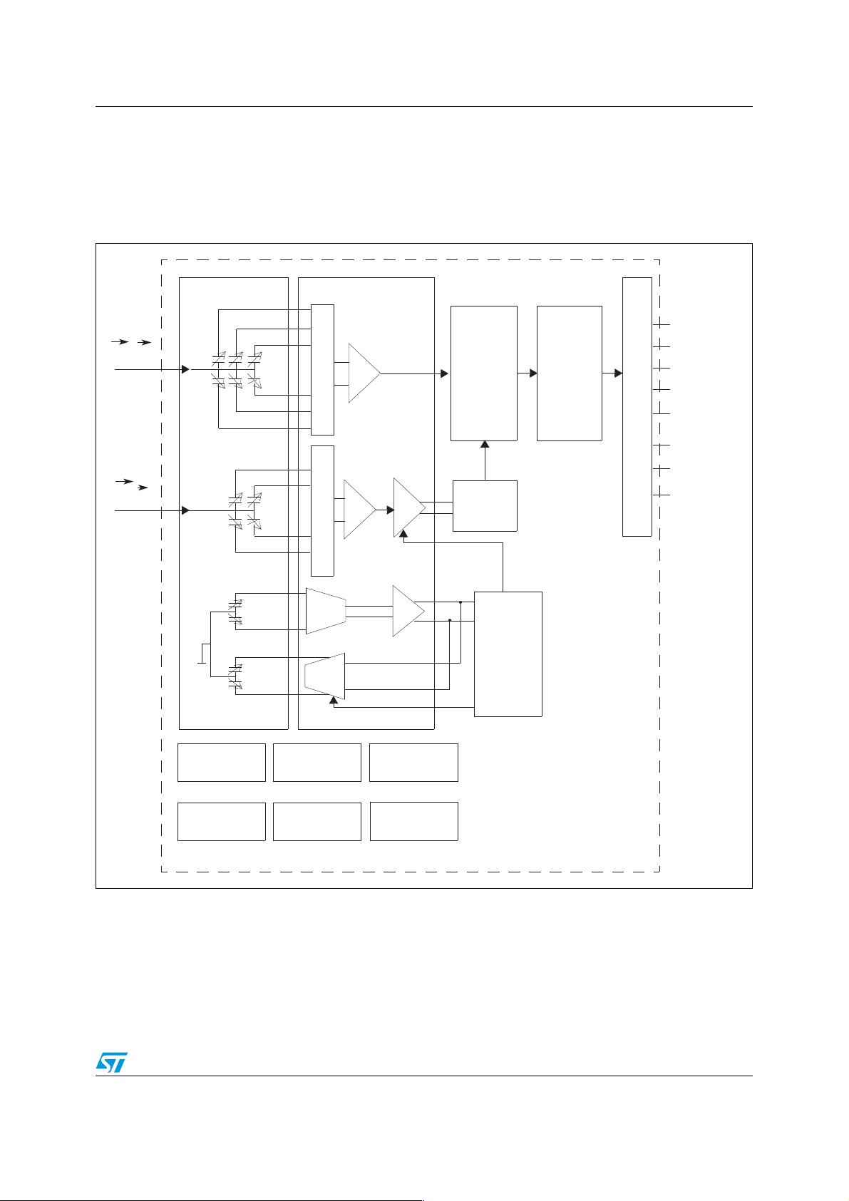
LSM320DL Block diagram and pin description
1 Block diagram and pin description
1.1 Block diagram
Figure 1. Block diagram
I (a)
I (Ω)
Sensing Block
Feedback+
Feedback-
Drive-
Drive+
X+
Sensing Interface
Y+
Z+
Z-
Y-
X-
X+
Z+
Z-
X-
MUX
MUX
VOLTAGE
GAIN
AMPLIFIER
CHARGE
AMPLIFIER
+
-
CHARGE
AMPLIFIER
+
-
DEMODULATOR
ANALOG
CONDITIONING
A/D Control
LOW-PASS
FILTER
AUTOMATIC
GAIN
CONTROL
Logicconverter
I2C/SPI
CS_A/G
SDA/SDI_A/G
SDO_A/G
INT1_A
INT2_A
INT_G
DRDY_G
SCL_A/G
REFERENCE
CONTROL LOGIC
&
INTERRUPT GEN.
TRIMMING
CIRCUITS
SET/RESET
CIRCUITS
CLOCK
PHASE
GENERATOR
AM09273V1
Doc ID 018845 Rev 1 9/53
Block diagram and pin description LSM320DL
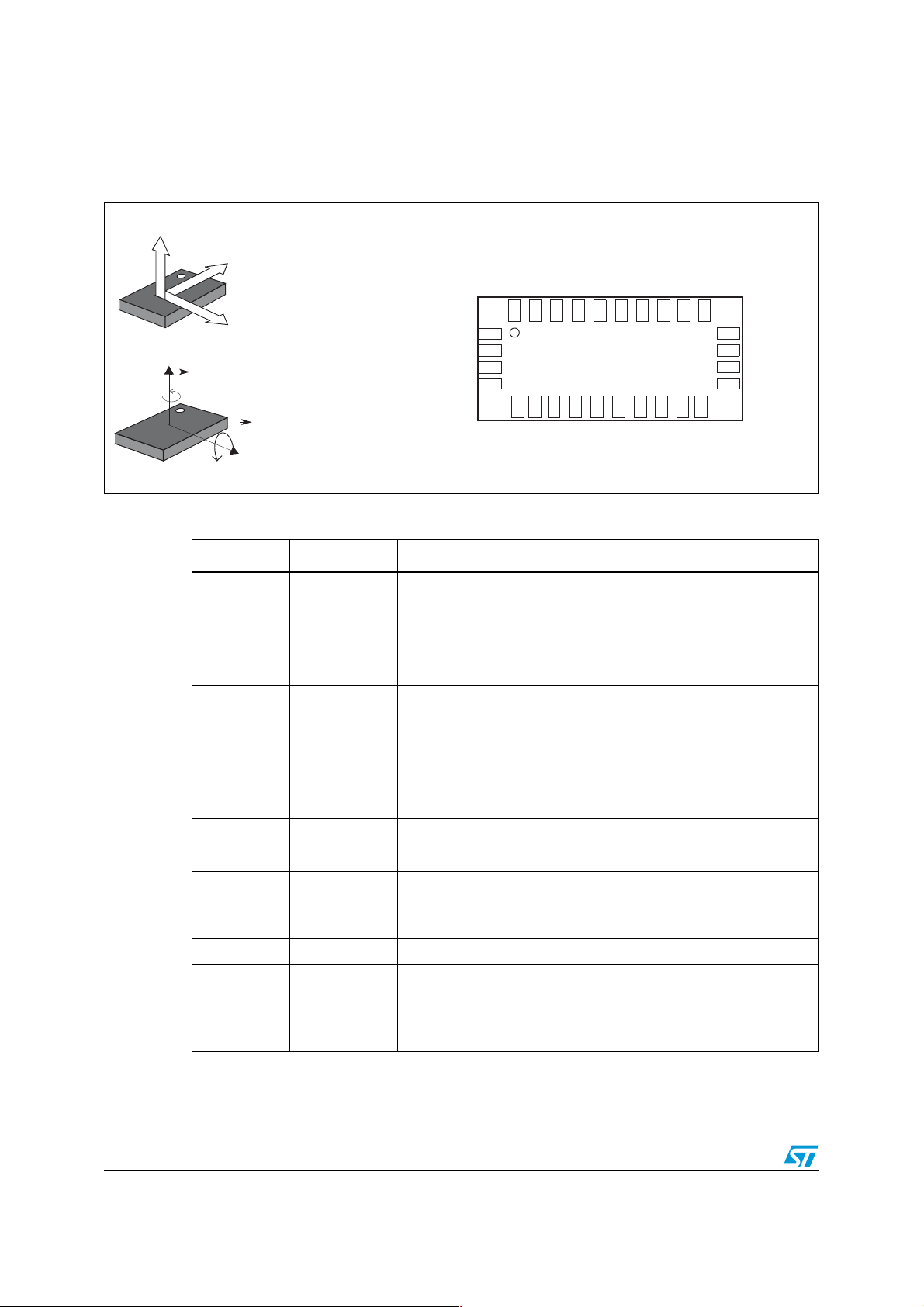
1.2 Pin description
Figure 2. Pin connection
Z
1
Z
+ Ω
Y
DIRECTION OF
DETECTABLE
X
z
1
ACCELERATIONS
DIRECTION OF
+Ω
DETECTABLE
X
VddIO_A
Res
VCONT
GND
28
25
ANGULAR RATE
X
Res
SDO_A
SDA/SDI_A
1
(BOTTOM VIEW)
24
Res
Res
Vdd
SCL_A
LSM320DL
INT_G
Res
DRDY_G
INT1_A
FILTVDD
FILTIN Y
Res
Res
SDO_G
INT2_A
CS_A
CS_G
SDA/SDI_G
10
Res
11
Vdd_IO_G
SCL_G
Res
14
15
Vdd
Res
AM09274V1
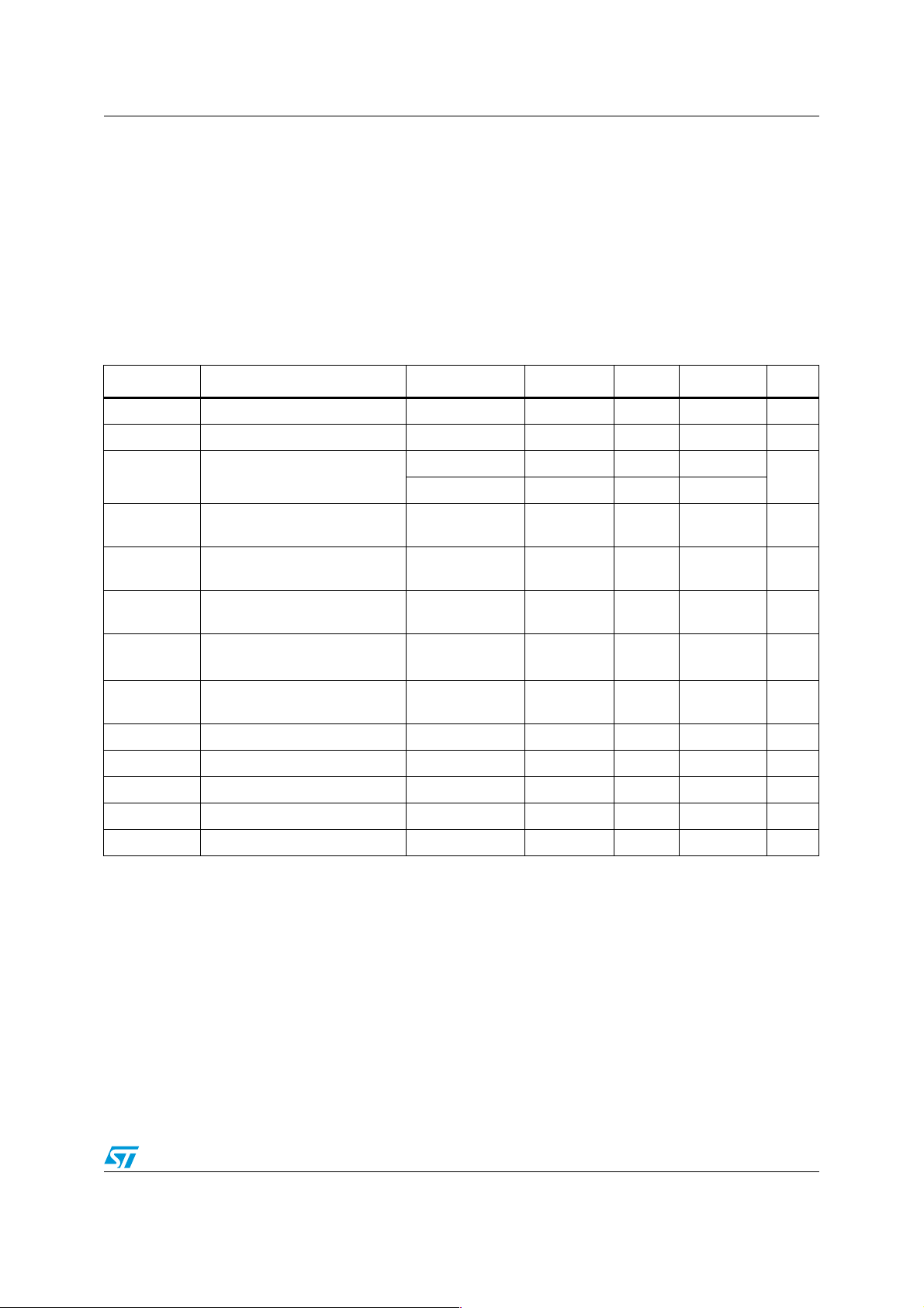
Table 2. Pin description
Pin# Name Function
Accelerometer:
1SDA/SDI_A
2 Res Reserved connect to GND
3SDO_A
4SCL_A
5 DRDY_G Gyroscope data ready
6 INT1_A Accelerometer interrupt signal
I2C serial data (SDA)
SPI serial data input (SDI)
3-wire interface serial data output (SDO)
Accelerometer:
SPI serial data output (SDO)
2
C least significant bit of the device address (SA0)
I
Accelerometer:
2
I
C serial clock (SCL)
SPI serial port clock (SPC)
Gyroscope:
7SDO_G
SPI serial data output (SDO)
2
C least significant bit of the device address (SA0)
I
8 INT2_A Accelerometer interrupt signal
Gyroscope:
9SDA/SDI_G
I2C serial data (SDA)
SPI serial data input (SDI)
3-wire interface serial data output (SDO)
10/53 Doc ID 018845 Rev 1
LSM320DL Block diagram and pin description
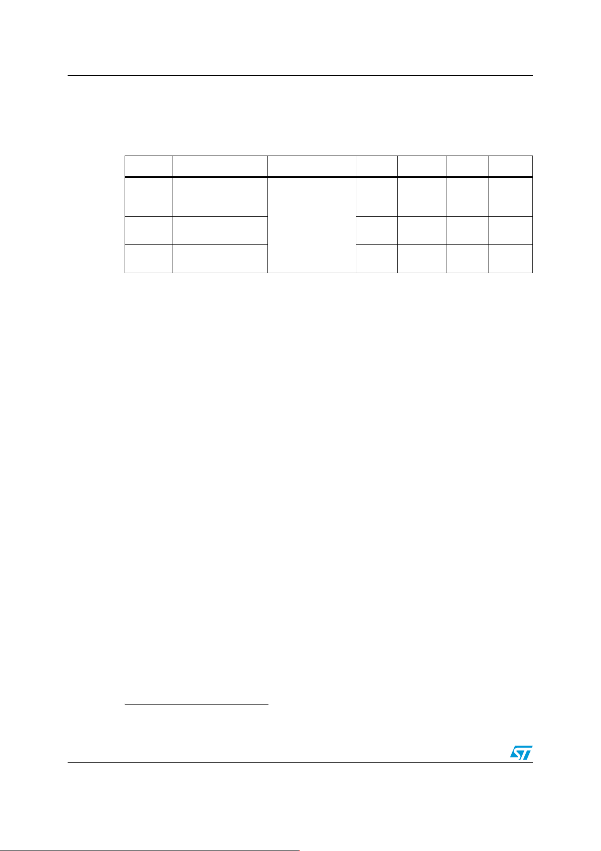
Table 2. Pin description (continued)
Pin# Name Function
Gyroscope:
10 CS_G
11 Res Reserved connect to GND
12 VddIO_G Gyroscope power supply for IO pins
13 SCL_G
14 Res Reserved connect to GND
15 Vdd Power supply
16 Res Reserved connect to GND
17 CS_A
18 Res Reserved connect to GND
19 Res Reserved connect to GND
SPI enable
2
C/SPI mode selection (1: SPI idle mode / I2C communication
I
enabled; 0: SPI communication mode / I2C disabled)
Gyroscope:
2
I
C serial clock (SCL)
SPI serial port clock (SPC)
Accelerometer:
SPI enable
2
C/SPI mode selection (1: SPI idle mode / I2C communication
I
enabled; 0: SPI communication mode / I
2
C disabled)
20 Res Reserved connect to GND
21 INT_G Gyroscope interrupt signal
22 Vdd Power supply
23 Res Reserved connect to GND
24 Res Reserved connect to GND
25 GND 0 V power supply
26 VCONT PLL filter connection
27 Res Reserved connect to GND
28 VddIO_A Accelerometer power supply for IO pins
Doc ID 018845 Rev 1 11/53
Module specifications LSM320DL
zHz
2 Module specifications
2.1 Mechanical characteristics
@ Vdd = 3V, T = 25 °C unless otherwise noted
Table 3. Mechanical characteristics
Symbol Parameter Test conditions Min. Typ.
FS bit set to 00 ±2.0
LA_FS
G_FS
LA_So
G_So Angular rate sensitivity
LA_So
G_So
LA_TyOff
G_TyOff Typical zero-rate level
LA_TCOff
G_TCOff
An Acceleration noise density
Rn Rate noise density FS bit set to 00 0.03 °/s/
Top Operating temperature range -40 +85 °C
Linear acceleration
measurement range
Angular rate
measurement range
Linear acceleration
sensitivity
Linear acceleration
sensitivity change vs.
temperature
Angular rate sensitivity
change vs. temperature
Typical Zero-g level offset
accuracy
Zerotemperature
Zero-rate level change vs.
temperature
(3)
g level change vs.
(2)
(2)
(4)
FS bit set to 01 ±4.0
FS bit set to 10 ±8.0
FS bit set to 11 ±16.0
FS bit set to 00 ±250
FS bit set to 10 ±2000
FS bit set to 00 1
FS bit set to 01 2
FS bit set to 10 4
FS bit set to 11 12
FS bit set to 00 8.75
FS bit set to 01 17.5
FS bit set to 10 70
FS bit set to 00 ±0.05 %/°C
From -40 to +85 °C ±2 %
FS bit set to 00 ±60 mg
FS bit set to 00 10 LSb
Max. delta from 25 °C ±0.5 m
FS bit set to 00
from -40 to +85 °C
FS bit set to 00
Normal mode, ODR bit set to
1001
(a)
.
(1)
Max. Unit
g
dpsFS bit set to 01 ±500
mg/digit
mdps/
digit
g/°C
±0.03 dps/°C
g/
220 µ
H
a. The product is factory calibrated at 3 V. The operational power supply range is from 2.4 V to 3.6 V.
12/53 Doc ID 018845 Rev 1
LSM320DL Module specifications
1. Typical specifications are not guaranteed.
2. Verified by wafer level test and measurement of initial offset and sensitivity.
3. Typical Zero-g level offset value after MSL3 preconditioning.
4. Offset can be eliminated by enabling the built-in high pass filter.
2.2 Electrical characteristics
@ Vdd = 3 V, T = 25 °C unless otherwise noted.
Table 4. Electrical characteristics
Symbol Parameter Test conditions Min. Typ.
Vdd Supply voltage 2.4 3.6 V
Vdd_IO Power supply for I/O 1.71 Vdd+0.1 V
(1)
Max. Unit
LA_Idd
LA_IddLowP
LA_IddPdn
G_Idd
G_IddSL
G_IddPdn
LA current consumption in
normal mode
LA current consumption in low
power mode
LA current consumption in
power-down mode
AR current consumption in
normal mode
Supply current
in sleep mode
(2)
AR current consumption in
power-down mode
ODR = 50Hz 11
ODR = 1Hz 2
ODR = 50Hz 6 µA
T = 25°C 0.5 µA
6mA
1.5 mA
T = 25 °C 5 µA
VIH Digital high level input voltage 0.8*Vdd_IO V
VIL Digital low level input voltage 0.2*Vdd_IO V
VOH High level output voltage 0.9*Vdd_IO V
VOL Low level output voltage 0.1*Vdd_IO V
Top Operating temperature range -40 +85 °C
1. Typical specifications are not guaranteed.
2. Sleep mode introduces a faster turn-on time compared to power-down mode.
µA
Doc ID 018845 Rev 1 13/53
Module specifications LSM320DL
2.3 Temperature sensor characteristics
@ Vdd =3.0 V, T= 25 °C, unless otherwise noted.
Table 5. Temperature sensor characteristics
Symbol Parameter Test condition Min. Typ.
Temperature sensor
TSDr
TODR
To p
1. Typical specifications are not guaranteed.
output change vs.
temperature
Temperature refresh
rate
Operating
temperature range
-
(b)
(1)
-1 °C/digit
1Hz
-40 +85 °C
Max. Unit
b. The product is factory calibrated at 3.0 V.
14/53 Doc ID 018845 Rev 1
LSM320DL Module specifications
t
t
t
t
t
t
t
t
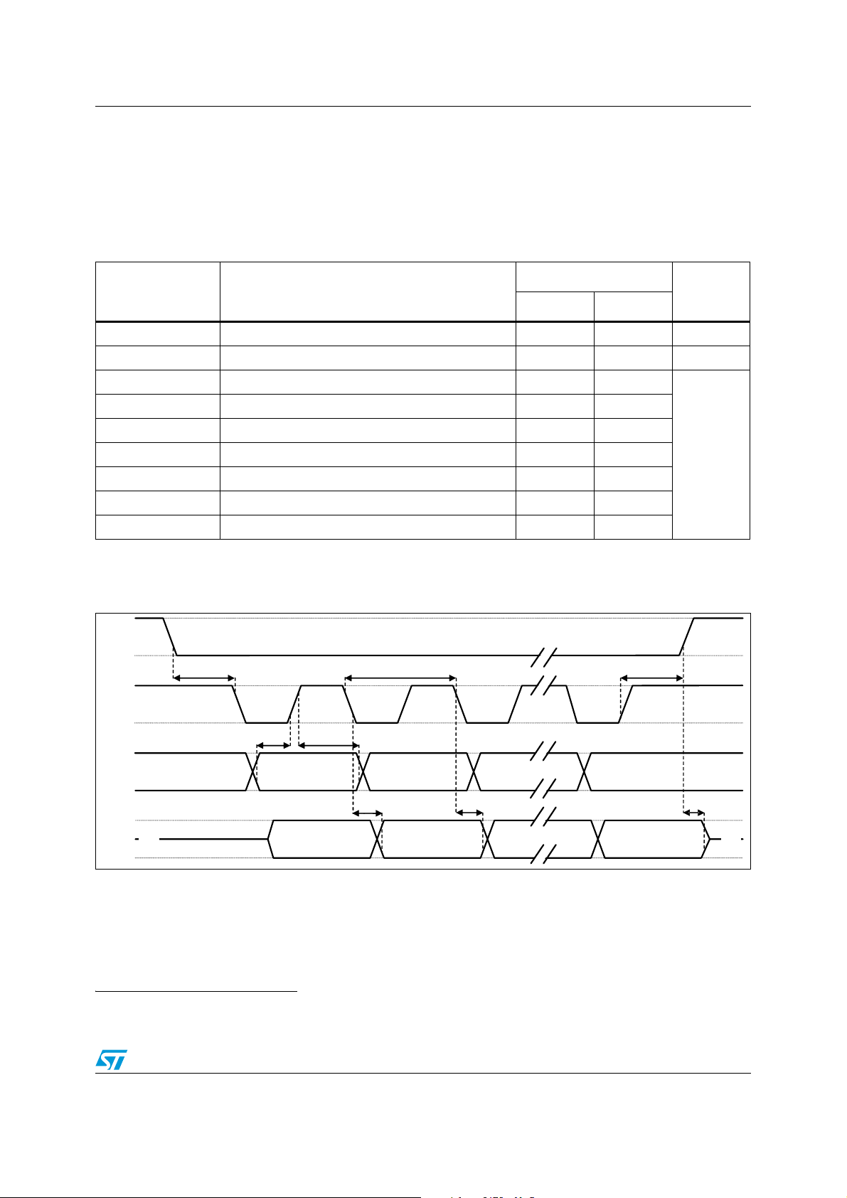
2.4 Communication interface characteristics
2.4.1 SPI - serial peripheral interface
Subject to general operating conditions for Vdd and Top.
Table 6. SPI slave timing values
(1)
Val ue
Symbol Parameter
Min. Max.
tc(SPC) SPI clock cycle 100 ns
fc(SPC) SPI clock frequency 10 MHz
tsu(CS) CS setup time 6
th(CS) CS hold time 8
tsu(SI) SDI input setup time 5
th(SI) SDI input hold time 15
tv(SO) SDO valid output time 50
th(SO) SDO output hold time 9
tdis(SO) SDO output disable time 50
Unit
ns
1. Values are guaranteed at 10 MHz clock frequency for SPI with both 4 and 3 wires, based on characterization results, not
tested in production.
(c)
h(SI)
h(CS)
LSB IN
LSB OUT
dis(SO)
v(SO)
c(SPC)
h(SO)
Figure 3. SPI slave timing diagram
CS
(3)
su(CS)
SPC
(3)
su(SI)
(3)
SDI
(3)
SDO
3. When no communication is on-going, data on CS, SPC, SDI, and SDO are driven by internal pull-up resistors.
MSB IN
MSB OUT
(3)
(3)
(3)
(3)
c. Measurement points are done at 0.2·Vdd_IO and 0.8·Vdd_IO, for both input and output ports.
Doc ID 018845 Rev 1 15/53
Module specifications LSM320DL
t
t
t
t
t
t
t
t
t
t
t
t
2.4.2 I2C - inter IC control interface
Subject to general operating conditions for Vdd and Top.
Table 7. I2C slave timing values
Symbol Parameter
I2C standard mode
(1)
I2C fast mode
Min. Max. Min. Max.
(1)
Unit
f
(SCL)
t
w(SCLL)
t
w(SCLH)
t
su(SDA)
t
h(SDA)
t
r(SDA) tr(SCL)
t
f(SDA) tf(SCL)
t
h(ST)
t
su(SR)
t
su(SP)
t
w(SP:SR)
1. Data based on standard I2C protocol requirement, not tested in production.
2. Cb = total capacitance of one bus line, in pF.
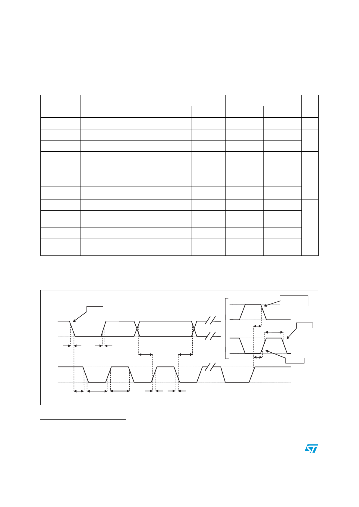
Figure 4. I
SCL clock frequency 0 100 0 400 KHz
SCL clock low time 4.7 1.3
SCL clock high time 4.0 0.6
SDA setup time 250 100 ns
SDA data hold time 0,01 3.45 0 0.9 µs
SDA and SCL rise time 1000
SDA and SCL fall time 300
START condition hold time 4 0.6
Repeated START condition
setup time
4.7 0.6
STOP condition setup time 4 0.6
Bus free time between STOP
and START condition
2
C slave timing diagram
(d)
4.7 1.3
20 + 0.1C
20 + 0.1C
b
b
(2)
(2)
µs
300
ns
300
µs
START
SDA
f(SDA)
r(SDA)
su(SDA)
h(SDA)
SCL
w(SCLL)
h(ST)
d. Measurement points are done at 0.2·Vdd_IO and 0.8·Vdd_IO, for both ports.
w(SCLH)
r(SCL)
f(SCL)
16/53 Doc ID 018845 Rev 1
su(SR)
su(SP)
w(SP:SR)
REPEATED
START
START
STOP
AM09238V1
 Loading...