

Ultra compact high performance e-compass
3D accelerometer and 3D magnetometer module
Features
■ 3 magnetic field channels and 3 acceleration
channels
■ From ±1.3 to ±8.1 gauss magnetic field full-
scale
■ ±2g/±4g/±8g/±16g selectable full-scale
■ 16 bit data output
2
■ I
C serial interface
■ Analog supply voltage 2.16 V to 3.6 V
■ Power-down mode/ low-power mode
■ 2 independent programmable interrupt
generators for free-fall and motion detection
■ Embedded temperature sensor
■ Embedded FIFO
■ 6D/4D orientation detection
■ ECOPACK
Applications
■ Compensated compass
■ Map rotation
■ Position detection
■ Motion-activated functions
■ Free-fall detection
■ Click/double click recognition
■ Pedometer
■ Intelligent power-saving for handheld devices
■ Display orientation
■ Gaming and virtual reality input devices
■ Impact recognition and logging
■ Vibration monitoring and compensation
Table 1. Device summary
®
RoHS and “Green” compliant
LSM303DLHC
Preliminary data
LGA-14
Description
The LSM303DLHC is a system-in-package
featuring a 3D digital linear acceleration sensor
and a 3D digital magnetic sensor.
LSM303DLHC has linear acceleration full-scales
of ±2g / ±4g / ±8g / ±16g and a magnetic field fullscale of ±1.3 / ±1.9 / ±2.5 / ±4.0 / ±4.7 / ±5.6 /
±8.1 gauss. All full-scales available are fully
selectable by the user.
LSM303DLHC includes an I
that supports standard and fast mode 100 kHz
and 400kHz. The system can be configured to
generate interrupt signals by inertial wakeup/free-fall events as well as by the position of the
device itself. Thresholds and timing of interrupt
generators are programmable by the end user on
the fly. Magnetic and accelerometer parts can be
enabled or put into power-down mode separately.
The LSM303DLHC is available in a plastic land
grid array package (LGA) and is guaranteed to
operate over an extended temperature range from
-40 °C to +85 °C.
(3x5x1mm)
2
C serial bus interface
Part number Temperature range [°C] Package Packing
LSM303DLHC -40 to +85 LGA-14 Tray
LSM303DLHCTR -40 to +85 LGA-14 Tape and reel
April 2011 Doc ID 018771 Rev 1 1/42
This is preliminary information on a new product now in development or undergoing evaluation. Details are subject to
change without notice.
www.st.com
42

Contents LSM303DLHC
Contents
1 Block diagram and pin description . . . . . . . . . . . . . . . . . . . . . . . . . . . . . 7
1.1 Block diagram . . . . . . . . . . . . . . . . . . . . . . . . . . . . . . . . . . . . . . . . . . . . . . . 7
1.2 Pin description . . . . . . . . . . . . . . . . . . . . . . . . . . . . . . . . . . . . . . . . . . . . . . 8
2 Module specifications . . . . . . . . . . . . . . . . . . . . . . . . . . . . . . . . . . . . . . . . 9
2.1 Sensor characteristics . . . . . . . . . . . . . . . . . . . . . . . . . . . . . . . . . . . . . . . . 9
2.2 Temperature sensor characteristics . . . . . . . . . . . . . . . . . . . . . . . . . . . . . 10
2.3 Electrical characteristics . . . . . . . . . . . . . . . . . . . . . . . . . . . . . . . . . . . . . . 11
2.4 Communication interface characteristics . . . . . . . . . . . . . . . . . . . . . . . . . 12
2.4.1 Sensor I2C - inter IC control interface . . . . . . . . . . . . . . . . . . . . . . . . . . 12
2.5 Absolute maximum ratings . . . . . . . . . . . . . . . . . . . . . . . . . . . . . . . . . . . . 13
2.6 Terminology . . . . . . . . . . . . . . . . . . . . . . . . . . . . . . . . . . . . . . . . . . . . . . . 14
2.6.1 Linear acceleration sensitivity . . . . . . . . . . . . . . . . . . . . . . . . . . . . . . . . 14
2.6.2 Zero-g level . . . . . . . . . . . . . . . . . . . . . . . . . . . . . . . . . . . . . . . . . . . . . . 14
3 Functionality . . . . . . . . . . . . . . . . . . . . . . . . . . . . . . . . . . . . . . . . . . . . . . 15
3.1 Factory calibration . . . . . . . . . . . . . . . . . . . . . . . . . . . . . . . . . . . . . . . . . . 15
4 Application hints . . . . . . . . . . . . . . . . . . . . . . . . . . . . . . . . . . . . . . . . . . . 16
4.1 External capacitors . . . . . . . . . . . . . . . . . . . . . . . . . . . . . . . . . . . . . . . . . . 16
4.2 Pull-up resistors . . . . . . . . . . . . . . . . . . . . . . . . . . . . . . . . . . . . . . . . . . . . 16
4.3 Digital interface power supply . . . . . . . . . . . . . . . . . . . . . . . . . . . . . . . . . . 17
4.4 Soldering information . . . . . . . . . . . . . . . . . . . . . . . . . . . . . . . . . . . . . . . . 17
4.5 High current wiring effects . . . . . . . . . . . . . . . . . . . . . . . . . . . . . . . . . . . . 17
5 Digital interfaces . . . . . . . . . . . . . . . . . . . . . . . . . . . . . . . . . . . . . . . . . . . 18
5.1 I2C serial interface . . . . . . . . . . . . . . . . . . . . . . . . . . . . . . . . . . . . . . . . . . 18
5.1.1 I2C operation . . . . . . . . . . . . . . . . . . . . . . . . . . . . . . . . . . . . . . . . . . . . . 19
5.1.2 Linear acceleration digital interface . . . . . . . . . . . . . . . . . . . . . . . . . . . . 20
5.1.3 Magnetic field digital interface . . . . . . . . . . . . . . . . . . . . . . . . . . . . . . . . 21
6 Register mapping . . . . . . . . . . . . . . . . . . . . . . . . . . . . . . . . . . . . . . . . . . 22
2/42 Doc ID 018771 Rev 1

LSM303DLHC Contents
7 Register description . . . . . . . . . . . . . . . . . . . . . . . . . . . . . . . . . . . . . . . . 24
7.1 Linear acceleration register description . . . . . . . . . . . . . . . . . . . . . . . . . . 24
7.1.1 CTRL_REG1_A (20h) . . . . . . . . . . . . . . . . . . . . . . . . . . . . . . . . . . . . . . 24
7.1.2 CTRL_REG2_A (21h) . . . . . . . . . . . . . . . . . . . . . . . . . . . . . . . . . . . . . . 25
7.1.3 CTRL_REG3_A (22h) . . . . . . . . . . . . . . . . . . . . . . . . . . . . . . . . . . . . . . 25
7.1.4 CTRL_REG4_A (23h) . . . . . . . . . . . . . . . . . . . . . . . . . . . . . . . . . . . . . . 26
7.1.5 CTRL_REG5_A (24h) . . . . . . . . . . . . . . . . . . . . . . . . . . . . . . . . . . . . . . 26
7.1.6 CTRL_REG6_A (25h) . . . . . . . . . . . . . . . . . . . . . . . . . . . . . . . . . . . . . . 27
7.1.7 REFERENCE/DATACAPTURE_A (26h) . . . . . . . . . . . . . . . . . . . . . . . . 27
7.1.8 STATUS_REG_A (27h) . . . . . . . . . . . . . . . . . . . . . . . . . . . . . . . . . . . . . 28
7.1.9 OUT_X_L_A (28h), OUT_X_H_A (29h) . . . . . . . . . . . . . . . . . . . . . . . . . 28
7.1.10 OUT_Y_L_A (2Ah), OUT_Y_H_A (2Bh) . . . . . . . . . . . . . . . . . . . . . . . . 28
7.1.11 OUT_Z_L_A (2Ch), OUT_Z_H_A (2Dh) . . . . . . . . . . . . . . . . . . . . . . . . 28
7.1.12 FIFO_CTRL_REG_A (2Eh) . . . . . . . . . . . . . . . . . . . . . . . . . . . . . . . . . . 29
7.1.13 FIFO_SRC_REG_A (2Fh) . . . . . . . . . . . . . . . . . . . . . . . . . . . . . . . . . . . 29
7.1.14 INT1_CFG_A (30h) . . . . . . . . . . . . . . . . . . . . . . . . . . . . . . . . . . . . . . . . 29
7.1.15 INT1_SRC_A (31h) . . . . . . . . . . . . . . . . . . . . . . . . . . . . . . . . . . . . . . . . 30
7.1.16 INT1_THS_A (32h) . . . . . . . . . . . . . . . . . . . . . . . . . . . . . . . . . . . . . . . . 31
7.1.17 INT1_DURATION_A (33h) . . . . . . . . . . . . . . . . . . . . . . . . . . . . . . . . . . . 31
7.1.18 INT2_CFG_A (34h) . . . . . . . . . . . . . . . . . . . . . . . . . . . . . . . . . . . . . . . . 31
7.1.19 INT2_SRC_A (35h) . . . . . . . . . . . . . . . . . . . . . . . . . . . . . . . . . . . . . . . . 32
7.1.20 INT2_THS_A (36h) . . . . . . . . . . . . . . . . . . . . . . . . . . . . . . . . . . . . . . . . 33
7.1.21 INT2_DURATION_A (37h) . . . . . . . . . . . . . . . . . . . . . . . . . . . . . . . . . . . 33
7.1.22 CLICK_CFG_A (38h) . . . . . . . . . . . . . . . . . . . . . . . . . . . . . . . . . . . . . . . 34
7.1.23 CLICK_SRC_A (39h) . . . . . . . . . . . . . . . . . . . . . . . . . . . . . . . . . . . . . . . 34
7.1.24 CLICK_THS_A (3Ah) . . . . . . . . . . . . . . . . . . . . . . . . . . . . . . . . . . . . . . . 35
7.1.25 TIME_LIMIT_A (3Bh) . . . . . . . . . . . . . . . . . . . . . . . . . . . . . . . . . . . . . . . 35
7.1.26 TIME_LATENCY_A (3Ch) . . . . . . . . . . . . . . . . . . . . . . . . . . . . . . . . . . . 35
7.1.27 TIME WINDOW_A (3Dh) . . . . . . . . . . . . . . . . . . . . . . . . . . . . . . . . . . . . 36
7.2 Magnetic field sensing register description . . . . . . . . . . . . . . . . . . . . . . . 36
7.2.1 CRA_REG_M (00h) . . . . . . . . . . . . . . . . . . . . . . . . . . . . . . . . . . . . . . . . 36
7.2.2 CRB_REG_M (01h) . . . . . . . . . . . . . . . . . . . . . . . . . . . . . . . . . . . . . . . . 37
7.2.3 MR_REG_M (02h) . . . . . . . . . . . . . . . . . . . . . . . . . . . . . . . . . . . . . . . . . 37
7.2.4 OUT_X_H_M (03), OUT_X_LH_M (04h) . . . . . . . . . . . . . . . . . . . . . . . . 38
7.2.5 OUT_Z_H_M (05), OUT_Z_L_M (06h) . . . . . . . . . . . . . . . . . . . . . . . . . 38
7.2.6 OUT_Y_H_M (07), OUT_Y_L_M (08h) . . . . . . . . . . . . . . . . . . . . . . . . . 38
7.2.7 SR_REG_M (09h) . . . . . . . . . . . . . . . . . . . . . . . . . . . . . . . . . . . . . . . . . 38
Doc ID 018771 Rev 1 3/42

Contents LSM303DLHC
7.2.8 IR_REG_M (0Ah/0Bh/0Ch) . . . . . . . . . . . . . . . . . . . . . . . . . . . . . . . . . . 38
7.2.9 TEMP_OUT_H_M (31h), TEMP_OUT_L_M (32h) . . . . . . . . . . . . . . . . 39
8 Package information . . . . . . . . . . . . . . . . . . . . . . . . . . . . . . . . . . . . . . . . 40
9 Revision history . . . . . . . . . . . . . . . . . . . . . . . . . . . . . . . . . . . . . . . . . . . 41
4/42 Doc ID 018771 Rev 1

LSM303DLHC List of tables
List of tables
Table 1. Device summary . . . . . . . . . . . . . . . . . . . . . . . . . . . . . . . . . . . . . . . . . . . . . . . . . . . . . . . . . . 1
Table 2. Pin description . . . . . . . . . . . . . . . . . . . . . . . . . . . . . . . . . . . . . . . . . . . . . . . . . . . . . . . . . . . 8
Table 3. Sensor characteristics . . . . . . . . . . . . . . . . . . . . . . . . . . . . . . . . . . . . . . . . . . . . . . . . . . . . . 9
Table 4. Temperature sensor characteristics . . . . . . . . . . . . . . . . . . . . . . . . . . . . . . . . . . . . . . . . . . 10
Table 5. Electrical characteristics . . . . . . . . . . . . . . . . . . . . . . . . . . . . . . . . . . . . . . . . . . . . . . . . . . . 11
Table 6. I
Table 7. Absolute maximum ratings . . . . . . . . . . . . . . . . . . . . . . . . . . . . . . . . . . . . . . . . . . . . . . . . . 13
Table 8. Accelerometer operating mode selection . . . . . . . . . . . . . . . . . . . . . . . . . . . . . . . . . . . . . . 15
Table 9. Serial interface pin description . . . . . . . . . . . . . . . . . . . . . . . . . . . . . . . . . . . . . . . . . . . . . . 18
Table 10. Serial interface pin description . . . . . . . . . . . . . . . . . . . . . . . . . . . . . . . . . . . . . . . . . . . . . . 18
Table 11. Transfer when master is writing one byte to slave . . . . . . . . . . . . . . . . . . . . . . . . . . . . . . . 19
Table 12. Transfer when master is writing multiple bytes to slave:. . . . . . . . . . . . . . . . . . . . . . . . . . . 19
Table 13. Transfer when master is receiving (reading) one byte of data from slave: . . . . . . . . . . . . . 19
Table 14. SAD+read/write patterns. . . . . . . . . . . . . . . . . . . . . . . . . . . . . . . . . . . . . . . . . . . . . . . . . . . 20
Table 15. Transfer when master is receiving (reading) multiple bytes of data from slave . . . . . . . . . 20
Table 16. SAD . . . . . . . . . . . . . . . . . . . . . . . . . . . . . . . . . . . . . . . . . . . . . . . . . . . . . . . . . . . . . . . . . . 21
Table 17. Register address map. . . . . . . . . . . . . . . . . . . . . . . . . . . . . . . . . . . . . . . . . . . . . . . . . . . . . 22
Table 18. CTRL_REG1_A register . . . . . . . . . . . . . . . . . . . . . . . . . . . . . . . . . . . . . . . . . . . . . . . . . . . 24
Table 19. CTRL_REG1_A description . . . . . . . . . . . . . . . . . . . . . . . . . . . . . . . . . . . . . . . . . . . . . . . . 24
Table 20. Data rate configuration . . . . . . . . . . . . . . . . . . . . . . . . . . . . . . . . . . . . . . . . . . . . . . . . . . . . 24
Table 21. CTRL_REG2_A register . . . . . . . . . . . . . . . . . . . . . . . . . . . . . . . . . . . . . . . . . . . . . . . . . . . 25
Table 22. CTRL_REG2_A description . . . . . . . . . . . . . . . . . . . . . . . . . . . . . . . . . . . . . . . . . . . . . . . . 25
Table 23. High pass filter mode configuration . . . . . . . . . . . . . . . . . . . . . . . . . . . . . . . . . . . . . . . . . . 25
Table 24. CTRL_REG3_A register . . . . . . . . . . . . . . . . . . . . . . . . . . . . . . . . . . . . . . . . . . . . . . . . . . . 25
Table 25. CTRL_REG3_A description . . . . . . . . . . . . . . . . . . . . . . . . . . . . . . . . . . . . . . . . . . . . . . . . 26
Table 26. CTRL_REG4_A register . . . . . . . . . . . . . . . . . . . . . . . . . . . . . . . . . . . . . . . . . . . . . . . . . . . 26
Table 27. CTRL_REG4_A description . . . . . . . . . . . . . . . . . . . . . . . . . . . . . . . . . . . . . . . . . . . . . . . . 26
Table 28. CTRL_REG5_A register . . . . . . . . . . . . . . . . . . . . . . . . . . . . . . . . . . . . . . . . . . . . . . . . . . . 26
Table 29. CTRL_REG5_A description . . . . . . . . . . . . . . . . . . . . . . . . . . . . . . . . . . . . . . . . . . . . . . . . 27
Table 30. CTRL_REG6_A register . . . . . . . . . . . . . . . . . . . . . . . . . . . . . . . . . . . . . . . . . . . . . . . . . . . 27
Table 31. CTRL_REG6_A description . . . . . . . . . . . . . . . . . . . . . . . . . . . . . . . . . . . . . . . . . . . . . . . . 27
Table 32. REFERENCE_A register . . . . . . . . . . . . . . . . . . . . . . . . . . . . . . . . . . . . . . . . . . . . . . . . . . 27
Table 33. REFERENCE_A register description . . . . . . . . . . . . . . . . . . . . . . . . . . . . . . . . . . . . . . . . . 28
Table 34. STATUS_A register . . . . . . . . . . . . . . . . . . . . . . . . . . . . . . . . . . . . . . . . . . . . . . . . . . . . . . 28
Table 35. STATUS_A register description . . . . . . . . . . . . . . . . . . . . . . . . . . . . . . . . . . . . . . . . . . . . . 28
Table 36. REFERENCE_A register . . . . . . . . . . . . . . . . . . . . . . . . . . . . . . . . . . . . . . . . . . . . . . . . . . 29
Table 37. REFERENCE_A register description . . . . . . . . . . . . . . . . . . . . . . . . . . . . . . . . . . . . . . . . . 29
Table 38. FIFO mode configuration . . . . . . . . . . . . . . . . . . . . . . . . . . . . . . . . . . . . . . . . . . . . . . . . . . 29
Table 39. FIFO_SRC_A register. . . . . . . . . . . . . . . . . . . . . . . . . . . . . . . . . . . . . . . . . . . . . . . . . . . . . 29
Table 40. INT1_CFG_A register . . . . . . . . . . . . . . . . . . . . . . . . . . . . . . . . . . . . . . . . . . . . . . . . . . . . . 29
Table 41. INT1_CFG_A description . . . . . . . . . . . . . . . . . . . . . . . . . . . . . . . . . . . . . . . . . . . . . . . . . . 29
Table 42. Interrupt mode . . . . . . . . . . . . . . . . . . . . . . . . . . . . . . . . . . . . . . . . . . . . . . . . . . . . . . . . . . 30
Table 43. INT1_SRC_A register . . . . . . . . . . . . . . . . . . . . . . . . . . . . . . . . . . . . . . . . . . . . . . . . . . . . . 30
Table 44. INT1_SRC_A description . . . . . . . . . . . . . . . . . . . . . . . . . . . . . . . . . . . . . . . . . . . . . . . . . . 30
Table 45. INT1_THS_A register . . . . . . . . . . . . . . . . . . . . . . . . . . . . . . . . . . . . . . . . . . . . . . . . . . . . . 31
Table 46. INT1_THS_A description . . . . . . . . . . . . . . . . . . . . . . . . . . . . . . . . . . . . . . . . . . . . . . . . . . 31
Table 47. INT1_DURATION_A register . . . . . . . . . . . . . . . . . . . . . . . . . . . . . . . . . . . . . . . . . . . . . . . 31
Table 48. INT1_DURATION_A description . . . . . . . . . . . . . . . . . . . . . . . . . . . . . . . . . . . . . . . . . . . . 31
2
C slave timing values . . . . . . . . . . . . . . . . . . . . . . . . . . . . . . . . . . . . . . . . . . . . . . . . . . . . 12
Doc ID 018771 Rev 1 5/42

List of tables LSM303DLHC
Table 49. INT2_CFG_A register . . . . . . . . . . . . . . . . . . . . . . . . . . . . . . . . . . . . . . . . . . . . . . . . . . . . . 31
Table 50. INT2_CFG_A description . . . . . . . . . . . . . . . . . . . . . . . . . . . . . . . . . . . . . . . . . . . . . . . . . . 32
Table 51. Interrupt mode . . . . . . . . . . . . . . . . . . . . . . . . . . . . . . . . . . . . . . . . . . . . . . . . . . . . . . . . . . 32
Table 52. INT2_SRC_A register . . . . . . . . . . . . . . . . . . . . . . . . . . . . . . . . . . . . . . . . . . . . . . . . . . . . . 32
Table 53. INT2_SRC_A description . . . . . . . . . . . . . . . . . . . . . . . . . . . . . . . . . . . . . . . . . . . . . . . . . . 33
Table 54. INT2_THS_A register . . . . . . . . . . . . . . . . . . . . . . . . . . . . . . . . . . . . . . . . . . . . . . . . . . . . . 33
Table 55. INT2_THS_A description . . . . . . . . . . . . . . . . . . . . . . . . . . . . . . . . . . . . . . . . . . . . . . . . . . 33
Table 56. INT2_DURATION_A register . . . . . . . . . . . . . . . . . . . . . . . . . . . . . . . . . . . . . . . . . . . . . . . 33
Table 57. INT2_DURATION_A description . . . . . . . . . . . . . . . . . . . . . . . . . . . . . . . . . . . . . . . . . . . . 33
Table 58. CLICK_CFG_A register . . . . . . . . . . . . . . . . . . . . . . . . . . . . . . . . . . . . . . . . . . . . . . . . . . . 34
Table 59. CLICK_CFG_A description . . . . . . . . . . . . . . . . . . . . . . . . . . . . . . . . . . . . . . . . . . . . . . . . . 34
Table 60. CLICK_SRC_A register . . . . . . . . . . . . . . . . . . . . . . . . . . . . . . . . . . . . . . . . . . . . . . . . . . . 34
Table 61. CLICK_SRC_A description . . . . . . . . . . . . . . . . . . . . . . . . . . . . . . . . . . . . . . . . . . . . . . . . . 34
Table 62. CLICK_THS_A register. . . . . . . . . . . . . . . . . . . . . . . . . . . . . . . . . . . . . . . . . . . . . . . . . . . . 35
Table 63. CLICK_SRC_A description . . . . . . . . . . . . . . . . . . . . . . . . . . . . . . . . . . . . . . . . . . . . . . . . . 35
Table 64. TIME_LIMIT_A register. . . . . . . . . . . . . . . . . . . . . . . . . . . . . . . . . . . . . . . . . . . . . . . . . . . . 35
Table 65. TIME_LIMIT_A description . . . . . . . . . . . . . . . . . . . . . . . . . . . . . . . . . . . . . . . . . . . . . . . . . 35
Table 66. TIME_LATENCY_A register . . . . . . . . . . . . . . . . . . . . . . . . . . . . . . . . . . . . . . . . . . . . . . . . 35
Table 67. TIME_LATENCY_A description . . . . . . . . . . . . . . . . . . . . . . . . . . . . . . . . . . . . . . . . . . . . . 36
Table 68. TIME_WINDOW_A register . . . . . . . . . . . . . . . . . . . . . . . . . . . . . . . . . . . . . . . . . . . . . . . . 36
Table 69. TIME_WINDOW_A description. . . . . . . . . . . . . . . . . . . . . . . . . . . . . . . . . . . . . . . . . . . . . . 36
Table 70. CRA_REG_M register . . . . . . . . . . . . . . . . . . . . . . . . . . . . . . . . . . . . . . . . . . . . . . . . . . . . 36
Table 71. CRA_REG_M description . . . . . . . . . . . . . . . . . . . . . . . . . . . . . . . . . . . . . . . . . . . . . . . . . . 36
Table 72. Data rate configurations . . . . . . . . . . . . . . . . . . . . . . . . . . . . . . . . . . . . . . . . . . . . . . . . . . . 36
Table 73. CRA_REG register . . . . . . . . . . . . . . . . . . . . . . . . . . . . . . . . . . . . . . . . . . . . . . . . . . . . . . . 37
Table 74. CRA_REG description . . . . . . . . . . . . . . . . . . . . . . . . . . . . . . . . . . . . . . . . . . . . . . . . . . . . 37
Table 75. Gain setting. . . . . . . . . . . . . . . . . . . . . . . . . . . . . . . . . . . . . . . . . . . . . . . . . . . . . . . . . . . . . 37
Table 76. MR_REG . . . . . . . . . . . . . . . . . . . . . . . . . . . . . . . . . . . . . . . . . . . . . . . . . . . . . . . . . . . . . . 37
Table 77. MR_REG description . . . . . . . . . . . . . . . . . . . . . . . . . . . . . . . . . . . . . . . . . . . . . . . . . . . . . 38
Table 79. SR register . . . . . . . . . . . . . . . . . . . . . . . . . . . . . . . . . . . . . . . . . . . . . . . . . . . . . . . . . . . . . 38
Table 80. SR register description . . . . . . . . . . . . . . . . . . . . . . . . . . . . . . . . . . . . . . . . . . . . . . . . . . . . 38
Table 81. IRA_REG_M . . . . . . . . . . . . . . . . . . . . . . . . . . . . . . . . . . . . . . . . . . . . . . . . . . . . . . . . . . . . 38
Table 82. IRB_REG_M . . . . . . . . . . . . . . . . . . . . . . . . . . . . . . . . . . . . . . . . . . . . . . . . . . . . . . . . . . . . 38
Table 83. IRC_REG_M . . . . . . . . . . . . . . . . . . . . . . . . . . . . . . . . . . . . . . . . . . . . . . . . . . . . . . . . . . . . 39
Table 84. TEMP_OUT_H_M register . . . . . . . . . . . . . . . . . . . . . . . . . . . . . . . . . . . . . . . . . . . . . . . . . 39
Table 85. TEMP_OUT_L_M register . . . . . . . . . . . . . . . . . . . . . . . . . . . . . . . . . . . . . . . . . . . . . . . . . 39
Table 86. TEMP_OUT resolution . . . . . . . . . . . . . . . . . . . . . . . . . . . . . . . . . . . . . . . . . . . . . . . . . . . . 39
Table 87. Revision history . . . . . . . . . . . . . . . . . . . . . . . . . . . . . . . . . . . . . . . . . . . . . . . . . . . . . . . . . 41
6/42 Doc ID 018771 Rev 1
LSM303DLHC Block diagram and pin description
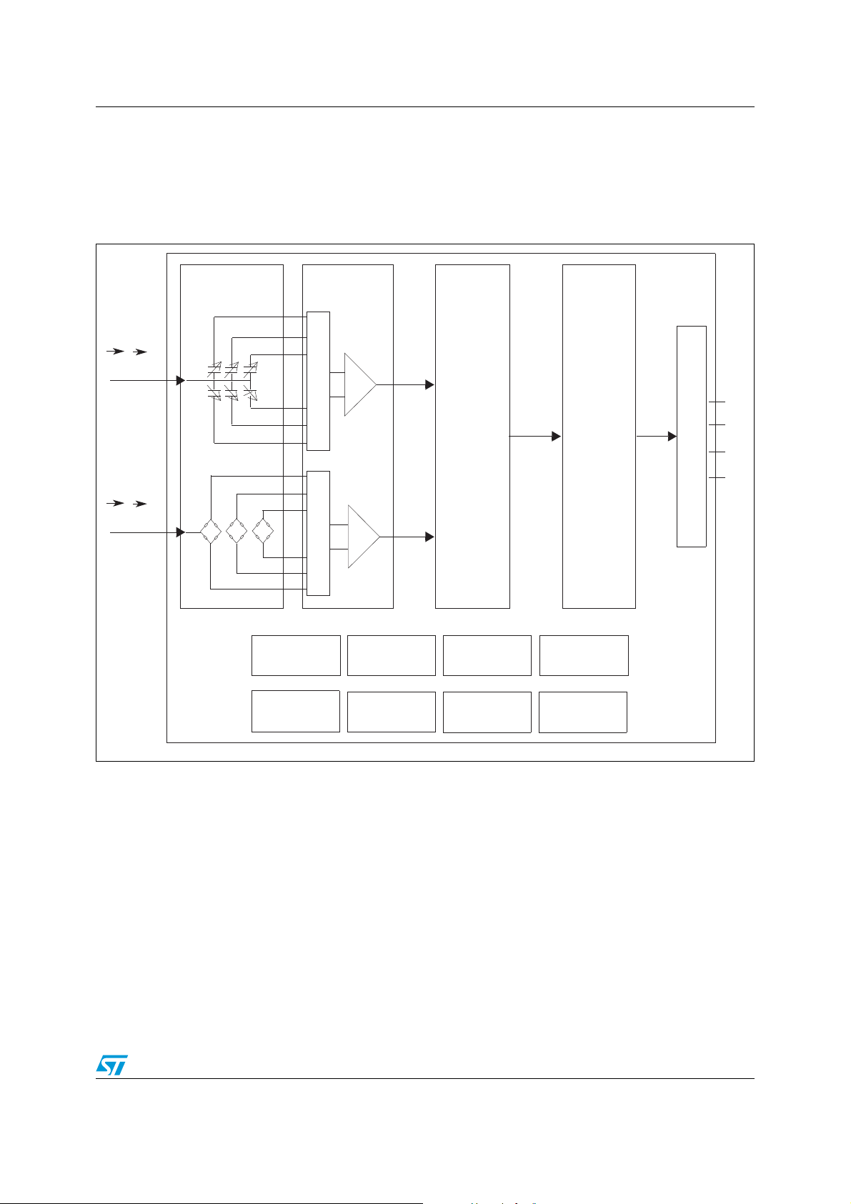
1 Block diagram and pin description
1.1 Block diagram
Figure 1. Block diagram
I (a)
I (M)
Sensing Block
Sensing Interface
X+
Y+
Z+
MUX
Z-
Y-
X-
X+
Y+
Z+
MUX
Z-
Y-
X-
INTERRUPT GEN.
CHARGE
AMPLIFIER
+
-
CHARGE
AMPLIFIER
+
-
REFERENCE
A/D Control
converter
TRIMMING
CIRCUITS
Logic
CLOCK
DI
I2C
SDA
SCL
INT1
INT2
FIFO
OFFSET
CIRCUITS
BUILT-IN
SET/RESET
CIRCUITS
TEMPERATURE
SENSOR
AM09236V1
Doc ID 018771 Rev 1 7/42
Block diagram and pin description LSM303DLHC
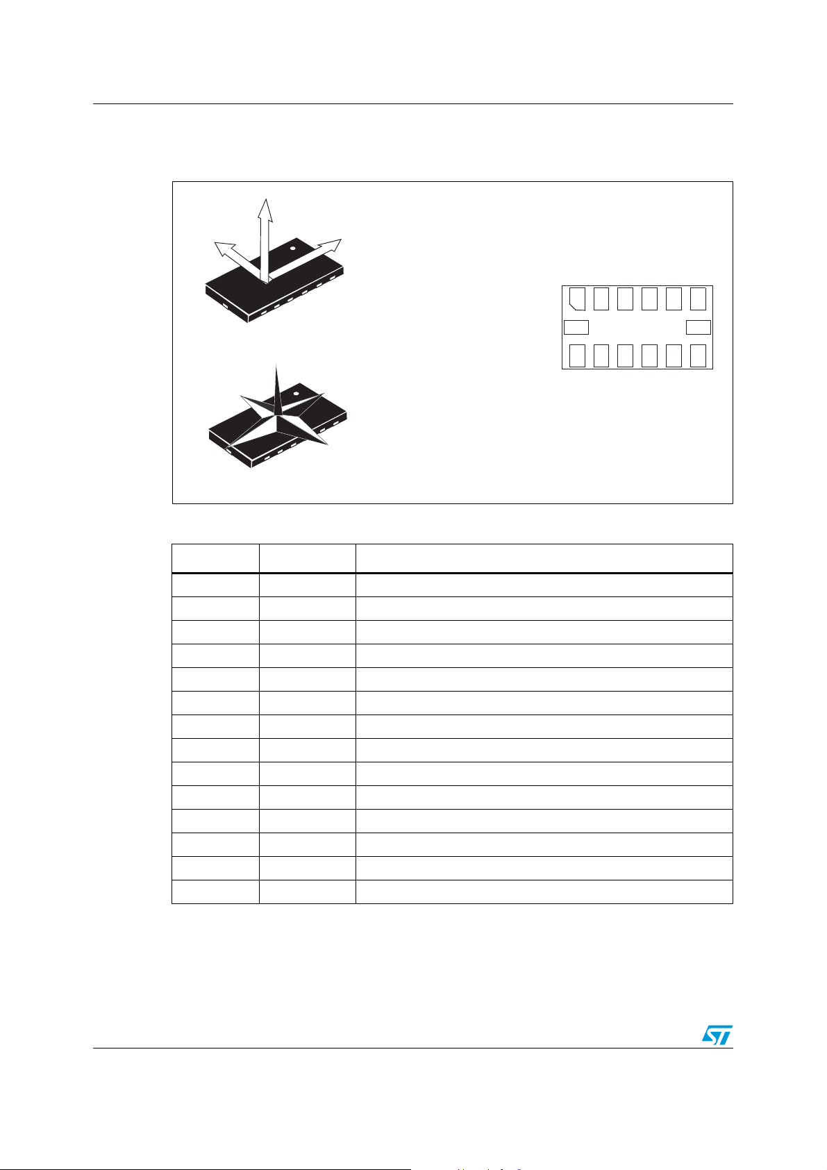
1.2 Pin description
Figure 2. Pin connection
Z
Y
6
TOP VIEW
Y
6
TOP VIEW
1
X
13
8
Z
1
X
13
8
DIRECTION OF
DETECTABLE
ACCELERATIONS
DIRECTION OF
DETECTABLE
MAGNETIC FIELDS
Table 2. Pin description
Pin# Name Function
1 Vdd_IO Power supply for I/O pins
2 SCL Signal interface I2C serial clock (SCL)
2
3 SDA Signal interface I
C serial data (SDA)
1
6
138
BOTTOM VIEW
AM09237V1
4 INT2 Inertial Interrupt 2
5 INT1 Inertial Interrupt 1
6 C1 Reserved capacitor connection (C1)
7 GND 0 V supply
8 Reserved Leave unconnected
9 DRDY Data ready
10 Reserved Connect to GND
11 Reserved Connect to GND
12 SETP S/R capacitor connection (C2)
13 SETC S/R capacitor connection (C2)
14 Vdd Power supply
8/42 Doc ID 018771 Rev 1
LSM303DLHC Module specifications
2 Module specifications
2.1 Sensor characteristics
@ Vdd = 2.5 V, T = 25 °C unless otherwise noted
Table 3. Sensor characteristics
Symbol Parameter Test conditions Min. Typ.
FS bit set to 00 ±2
LA_FS
M_FS Magnetic measurement range
LA_So Linear acceleration sensitivity
M_GN Magnetic gain setting
Linear acceleration
measurement range
(2)
FS bit set to 01 ±4
FS bit set to 10 ±8
FS bit set to 11 ±16
GN bits set to 001 ±1.3
GN bits set to 010 ±1.9
GN bits set to 011 ±2.5
GN bits set to 100 ±4.0
GN bits set to 101 ±4.7
GN bits set to 110 ±5.6
GN bits set to 111 ±8.1
FS bit set to 00 1
FS bit set to 01 2
FS bit set to 10 4
FS bit set to 11 12
GN bits set to 001 (X,Y) 1100
GN bits set to 001 (Z) 980
GN bits set to 010 (X,Y) 855
GN bits set to 010 (Z) 760
GN bits set to 011 (X,Y) 670
GN bits set to 011 (Z) 600
GN bits set to 100 (X,Y) 450
GN bits set to 100 (Z) 400
GN bits set to 101 (X,Y) 400
GN bits set to 101 (Z) 355
GN bits set to 110 (X,Y) 330
GN bits set to 110 (Z) 295
GN bits set to 111
GN bits set to 111
(a)
.
(2)
(X,Y) 230
(2)
(Z) 205
(1)
Max. Unit
g
gauss
mg/LSB
LSB/
gauss
a. The product is factory calibrated at 2.5 V. The operational power supply range is from 2.16 V to 3.6 V.
Doc ID 018771 Rev 1 9/42
Module specifications LSM303DLHC
Table 3. Sensor characteristics (continued)
Symbol Parameter Test conditions Min. Typ.
(1)
Max. Unit
LA_TCSo
Linear acceleration sensitivity
change vs. temperature
FS bit set to 00 ±0.01 %/°C
Linear acceleration typical
LA_TyOff
LA_TCOff
g level offset
Zero-
accuracy
Linear acceleration Zero-
(3),(4)
g
level change vs. temperature
FS bit set to 00 ±60 mg
Max. delta from 25 °C ±0.5 m
FS bit set to 00, normal
LA_An Acceleration noise density
mode(Table 8.), ODR bit
220
set to 1001
M_R Magnetic resolution 2 mgauss
M_CAS Magnetic cross-axis sensitivity
M_EF Maximum exposed field
Cross field =.0.5 gauss
H applied = ±3 gauss
No permitting effect on
zero reading
±1
10000 gauss
Sensitivity starts to
M_DF Disturbing field
degrade. Use S/R pulse to
20 gauss
restore sensitivity
Top Operating temperature range -40 +85 °C
1. Typical specifications are not guaranteed.
2. Verified by wafer level test and measurement of initial offset and sensitivity.
3. Typical Zero-g level offset value after MSL3 preconditioning.
4.
Offset can be eliminated by enabling the built-in high pass filter.
g/°C
ug/
sqrt(Hz)
%FS/
gauss
2.2 Temperature sensor characteristics
@ Vdd = 2.5 V, T = 25 °C unless otherwise noted
Table 4. Temperature sensor characteristics
Symbol Parameter Test condition Min. Typ.
TSDr
TODR Temperature refresh rate ODR
Top Operating temperature range -40 +85 °C
1. Typical specifications are not guaranteed.
2. 12-bit resolution.
3. For ODR configuration refer to Table 72.
10/42 Doc ID 018771 Rev 1
Temperature sensor output
change vs. temperature
-
b. The product is factory calibrated at 2.5 V.
(b)
.
(1)
8LSB/°C
(3)
Max. Unit
(2)
Hz
LSM303DLHC Module specifications
2.3 Electrical characteristics
@ Vdd = 2.5 V, T = 25 °C unless otherwise noted.
Table 5. Electrical characteristics
Symbol Parameter
Vdd Supply voltage
Test
conditions
Min. Typ.
2.16 3.6 V
(1)
Vdd_IO Module power supply for I/O 1.71 1.8 Vdd+0.1
Idd
IddSL
Current consumption in normal
mode
(2)
Current consumption in
sleep-mode
(3)
-
110 µA
1µA
Top Operating temperature range -40 +85
1. Typical specifications are not guaranteed.
Magnetic sensor setting ODR = 7.5 Hz, Accelerometer sensor ODR = 50 Hz.
2.
Linear accelerometer in sleep-mode and magnetic sensor in power-down mode.
3.
Max. Unit
°C
Doc ID 018771 Rev 1 11/42
Module specifications LSM303DLHC
t
t
t
t
t
t
t
t
t
t
t
t
2.4 Communication interfaces characteristics
External pull-up resistors are required to support I2C standard and fast speed modes.
2.4.1 Sensor I2C - inter IC control interface
Subject to general operating conditions for Vdd and Top.
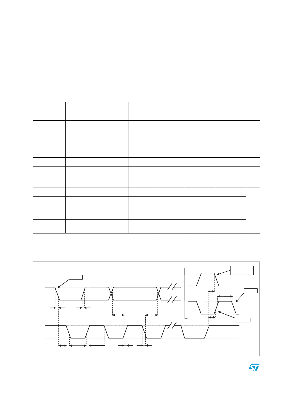
Table 6. I2C slave timing values
Symbol Parameter
I2C standard mode
(1)
I2C fast mode
Min. Max. Min. Max.
(1)
Unit
f
(SCL)
t
w(SCLL)
t
w(SCLH)
t
su(SDA)
t
h(SDA)
t
r(SDA) tr(SCL)
t
f(SDA) tf(SCL)
t
h(ST)
t
su(SR)
t
su(SP)
t
w(SP:SR)
1. Data based on standard I2C protocol requirement, not tested in production.
2. Cb = total capacitance of one bus line, in pF.
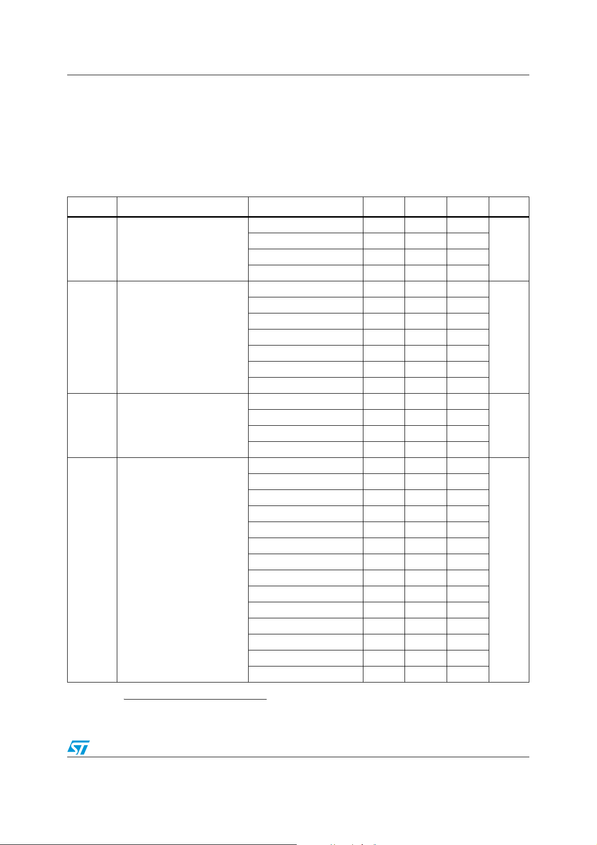
Figure 3. I
SCL clock frequency 0 100 0 400 KHz
SCL clock low time 4.7 1.3
SCL clock high time 4.0 0.6
SDA setup time 250 100 ns
SDA data hold time 0.01 3.45 0.01 0.9 µs
SDA and SCL rise time 1000
SDA and SCL fall time 300
START condition hold time 4 0.6
Repeated START condition
setup time
4.7 0.6
STOP condition setup time 4 0.6
Bus free time between STOP
and START condition
2
C slave timing diagram
(c)
4.7 1.3
20 + 0.1C
20 + 0.1C
µs
(2)
b
(2)
b
300
ns
300
µs
START
SDA
f(SDA)
r(SDA)
su(SDA)
h(SDA)
SCL
w(SCLL)
h(ST)
w(SCLH)
r(SCL)
f(SCL)
12/42 Doc ID 018771 Rev 1
su(SR)
su(SP)
w(SP:SR)
REPEATED
START
START
STOP
AM09238V1
LSM303DLHC Module specifications
2.5 Absolute maximum ratings
Stresses above those listed as “absolute maximum ratings” may cause permanent damage
to the device. This is a stress rating only and functional operation of the device under these
conditions is not implied. Exposure to maximum rating conditions for extended periods may
affect device reliability.
Table 7. Absolute maximum ratings
Symbol Ratings Maximum value Unit
Vdd Supply voltage -0.3 to 4.8 V
Vdd_IO I/O pins supply voltage -0.3 to 4.8 V
Vin Input voltage on any control pin (SCL, SDA) -0.3 to Vdd_IO +0.3 V
A
A
T
POW
UNP
T
OP
STG
Acceleration (any axis, powered, Vdd = 2.5 V)
Acceleration (any axis, unpowered)
Operating temperature range -40 to +85 °C
Storage temperature range -40 to +125 °C
3,000 for 0.5 ms g
10,000 for 0.1 ms g
3,000 for 0.5 ms g
10,000 for 0.1 ms g
This is a mechanical shock sensitive device, improper handling can cause permanent
damage to the part.
This is an ESD sensitive device, improper handling can cause permanent damage to
the part.
c. Measurement points are done at 0.2·Vdd_IO and 0.8·Vdd_IO, for both ports.
Doc ID 018771 Rev 1 13/42
 Loading...