

LS404
HIGH PERFORMANCE
QUAD OPERATIONAL AMPLIFIER
■ SINGLE OR SPLIT SUPPLY OPERATION
■ LOW POWER CONSUMPTION
■ SHORT CIRCUIT PROTECTION
■ LOW DISTORTION, LOW NOISE
■ HIGH GAIN-BANDWIDTH PRODUCT
■ HIGH CHANNEL SEPARATION
DESCRIPTION
The LS404 is a high performance quad operational amplifier with frequenc y and phas e compe nsation built into the chip. The internal phase compensation allows stable operation as voltage follower
in spite of its high Gain-Bandwidth Product.
The circuit presents very stable electrical characteristics over the entire supply voltage range, and
is particularly intended for professional and telecom applications (active filter, etc).
The patented input stage circuit allows small input
signal swings below the negative supply voltage
and prevents phase inversion when the inputs are
over drivers.
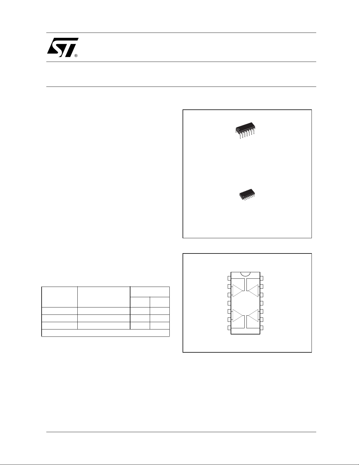
N
DIP14
(Plastic Package)
D
SO14
(Plastic Micropacka ge)
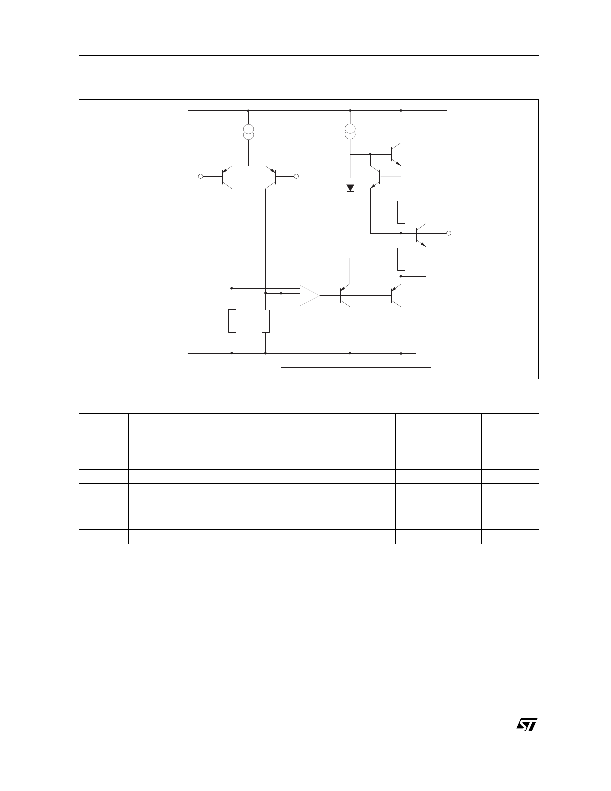
PIN CONNECTIONS (top view)
ORDER CODE
Part Number Temperature Range
LS404C 0°C, +70°C
LS404I -40°C, +105°C
LS404M -55°C, +125°C
Example : LS204CN
N = Dual in Line Package (D IP)
D = Small Outline Package (SO) - also available in Tape & Reel (DT)
November 2001
Package
ND
••
••
••
Output 1
Inverting Input 1
Non-inverting Input 1
V
CC
Non-inverting Input 2
Inverting Input 2
Output 2
1
2
-
+
3
+
4
5
+
-
6
7
14
13
-
+
12
11
10
+
9
8
Output 4
Inverting Input 4
Non-inverting Input 4
-
V
CC
Non-inverting Input 3
Inverting Input 3
Output 3
1/11
LS404
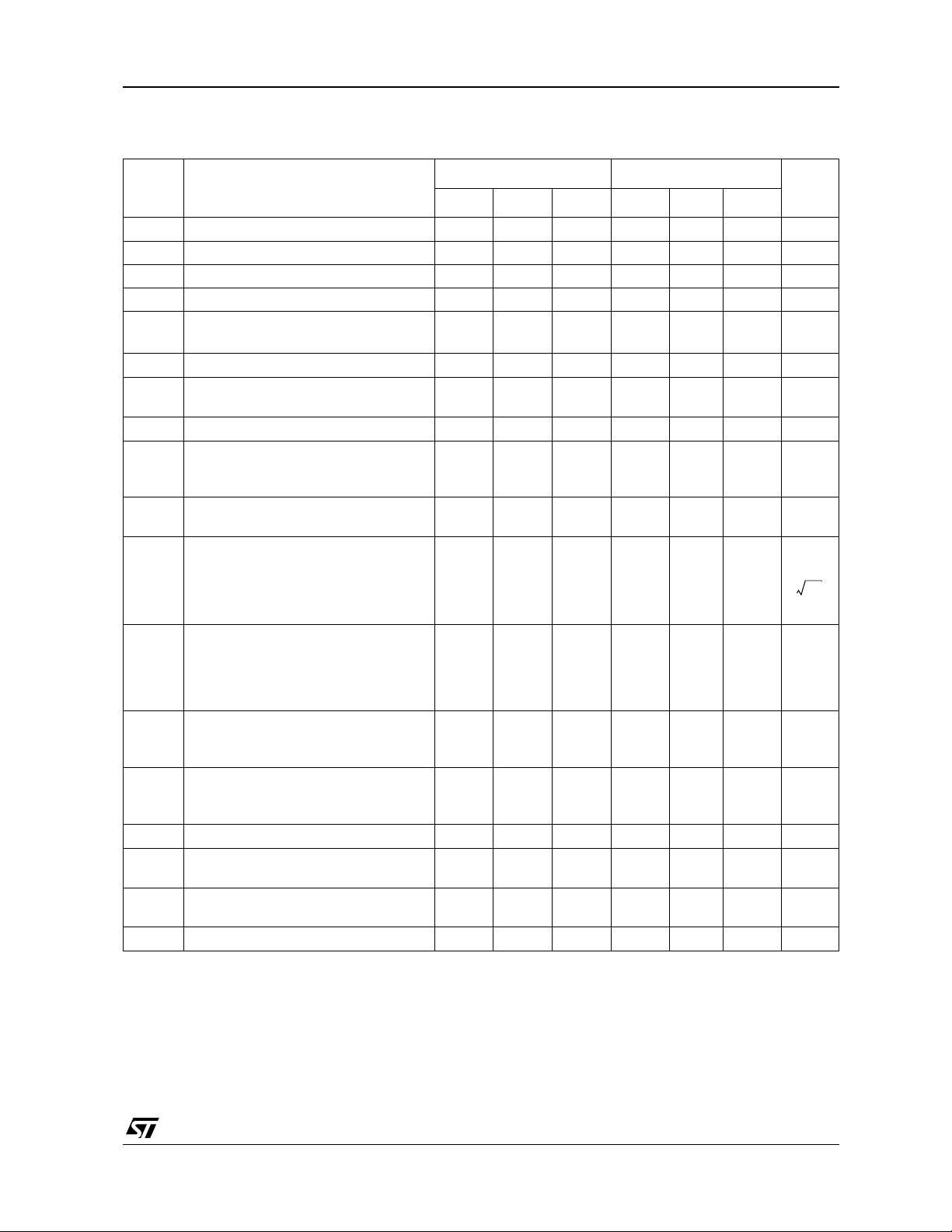
SCHEMATIC DIAGRAM (1/4 LS404)
Inverting input
Non-inverting
input
Output
ABSOLUTE MAXIMUM RATINGS
Symbol Parameter Value Unit
V
T
V
V
oper
P
T
Supply voltage ±18 V
CC
Input Voltage Positive
i
Differential Input Voltage
id
Negative
Operating Temperature Range LS204C
LS204I
LS204I
Power Dissipation at T
tot
Storage Temperature Range -65 to +150 °C
stg
amb
= 70°C
+V
CC
-VCC - 0.5
±(V
-1)
CC
0 to +70
-40 to +105
-55 to +125
400 mW
V
V
°C
2/11
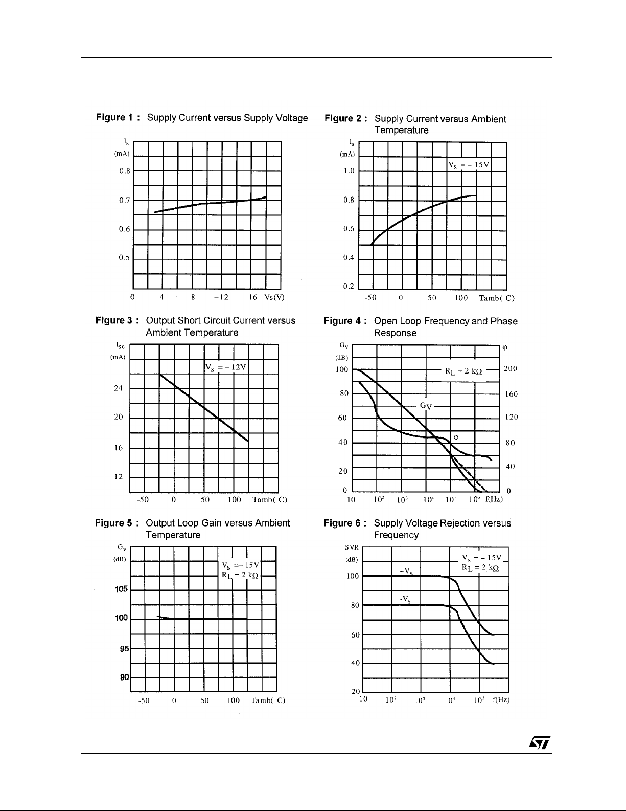
ELECTRICAL CHARACTERISTICS
V
= ±15V, T
CC
Symbol Parameter
I
Supply Current 1.3 2 1.5 3 mA
cc
Input Bias Current
I
ib
R
Input Resistance (f = 1kHz) 1 1 M
i
Input Offset Voltage (Rs ≤ 10kΩ)
V
io
DV
Input Offset Voltage Drift (Rs ≤ 10kΩ)
io
Input Offset Current
I
io
Input Offset Current Drift
DI
io
I
Output Short-circuit Current 23 23 mA
os
Large Signal Voltage Gain
A
vd
GBP
Gain Bandwith Product
Equivalent Input Noise Voltage
e
n
Total Harmonic Distortion
THD
Output Voltage Swing
±V
opp
Large Signal Voltage Swing
V
opp
Slew Rate (R
SR
SVR
CMR
V
o1/Vo2
Supply Voltage Rejection Ratio
Common Mode Rejection Ratio
Channel Separation (f= 1kHz) 100 120 120 dB
= 25°C (unless otherwise specified)
amb
T
< Top < T
min
< Top < T
T
min
R
= 2kΩ, VCC = ±15V
L
V
= ±4V
CC
f =100kHz, R
max
max
= 2k, CL = 100pF
L
f = 1kHz,
= 50
R
Ω
s
R
= 1k
Ω
s
= 10k
R
Ω
s
Unity Gain
= 2k
Ω,
Vo = 2V
pp
R
L
f = 1kHz
f = 20kHz
= 2kΩ, VCC = ±15V
R
L
V
= ±4V
CC
f = 10kHz, R
= 1k
R
L
V
= 1V, f = 100Hz
ic
V
= 10V
ic
= 10k
Ω
L
Ω
= 2kΩ, unity gain)
L
LS404
LS404I - LS404M LS404C
Min. Typ. Max. Min. Typ. Max.
50 200 100 300 nA
0.7 2.5 0.5 5 mV
55
10 40 20 80 nA
0.08 0.1 nA/°C
90
100
95
86 100
95
1.8 3 1.5 2.5 MHz
8
10
18
0.01
0.03
±13
±3
22
20
15 10
12
20
0.4 0.01
0.03
±13
±3
22
20
0.8 1.5 1 V/µs
90 94 86 90
90 94 86 90
Unit
µV/°C
dB
nV
----------- -
Vpp
dB
dB
Ω
Hz
%
V
3/11
LS404
4/11

LS404
5/11

LS404
APPLICATION INFORMATION: Active low-pass filter
BUTTERWORTH
The Butterworth is a "maximally flat" amplitude response filter (figure 10) Butterworth filters are
used for filtering signals in data acquisition systems to prevent aliasing errors in samples-data
applications and for ge neral purpose l ow-pass filtering.
The cut-off frequency Fc, is the frequency at which
the amplitude response is down 3d B. The attenuation rate beyond the cutoff frequency is n6 dB per
octave of frequency where n is t he orde r (num ber
of poles) of the filter.
Other characteristics :
❑ Flattest possible amplitude response
❑ Excellent gain accuracy at low frequency
end of passband
BESSEL
The Bessel is a type of “linear ph ase” filter. Because of their linear phase characteristics, these
filters approximate a constant time delay over a
limited frequency range. Be ssel filters pass transient waveforms with a minimum of distortion.
They are also used to provide time delays for low
pass filtering of modulated waveforms and as a
“running average” type filter.
The maximum phase shift is radians where
n is the order (number of poles) of the filter. The
cut-off frequency fc, is defined as the frequency at
which the phase shift is one half of this value.
The table below shows the typical overshoot and setting time response of the low pass filters to a step
input.
Butterworth
Bessel
Chebyschev (ripple ±0.25dB)
Chebyschev (ripple ±1dB)
n
π–
---------- 2
Number of Poles
2
4
6
8
2
4
6
8
2
4
6
8
2
4
6
8
For accurate delay, the cut-off frequency should
be twice the maximum signal frequency.
The following table can be used to obtain the -3dB
frequency of the filter.
2 Pole 4 Pole 6 Pole 8 Pole
-3dB Frequency 0.77fc 0.67fc 0.57fc 0.50fc
Other characteristics :
❑ Selectivity not as great as Chebyschev or
Butterworth
❑ V ery little overshoot response to step inputs
❑ Fast rise time
CHEBYSCHEV
Chebyschev filters have greater selectivity than either Bessel ro Butterworth at the expense of ripple
in the passband (figure 11).
Chebyschev filters are normally designed with
peak-to-peak ripple values from 0.2dB to 2dB.
Increased ripple in the passband allows increased
attenuation above the cut-off frequency.
The cut-off frequ ency is defin ed as the frequency
at which the amplitude res ponse passes through
the specificed maximum ripple band and enters
the stop band.
Other characteristics :
❑ Greater selectivity
❑ Very non-linear phase response
❑ High overshoot response to step inputs
Peak
Overshoot
% Overshoot ±1% ±0.1% ±0.01%
4
11
14
14
0.4
0.8
0.6
0.1
11
18
21
23
21
28
32
34
Settling Time (% of final value)
1.1Fc sec.
1.7/fc
2.4/fc
3.1/fc
0.8/fc
1.0/fc
1.3/fc
1.6/fc
1.1/fc
3.0/fc
5.9/fc
8.4/fc
1.6/fc
4.8/fc
8.2/fc
11.6/fc
1.7Fc sec.
2.8/fc
3.9S/fc
5.1/fc
1.4/fc
1.8/fc
2.1/fc
2.3/fc
1.6/fc
5.4/fc
10.4/fc
16.4/fc
2.7/fc
8.4/fc
16.3/fc
24.8/fc
1.9Fc sec.
3.8/fc
5.0S/fc
7.1/fc
1.7/fc
2.4/fc
2.7/fc
3.2/fc
-
-
-
-
-
-
-
Design of 2nd order acti ve low pass f ilt er (Sallen a nd Key configuration uni ty gain op-am p)
6/11

Fixed R = R1 = R2, we have (see figure 13)
1
----
R
-------
ω
ζ
c
C
1 =
Figure 13 : Filter Configuration
C
2 =
C2
1
----
R
1
-----------
ξω
LS404
c
Vin
Three parameters are needed to characterize the
frequency and phase respons e o f a 2n d order active filter: the gain (Gv), the da mping factio (ξ) or
the Q factor (Q = 2 ξ)
1
), and the cuttoff f requency
(fc).
R2R1
C1
Vout
The higher order response are obtained with a series of 2nd order sections. A simple RC section is
introduced when an odd filter is required.
The choice of ’ξ' (or Q factor) determines the filter
response (see table 1).
Table 1
Filter Response
Bessel
Butterworth Frequency at which Gv = -3dB
Chebyschev
------ -
------ -
------ -
ξ
3
2
2
2
2
2
Q Cuttoff Frequency fc
Frequency at which Phase Shift is -90°C
1
------ 3
1
------ 2
Frequency at which the amplitude response
passes through specified max. ripple band and
1
------ 2
enters the stop bank.
EXAMPLE
Figure 14 : 5th Order Low-pass Filter (Butterworth) with Unity Gain configuration
C2
Ri
Ci
R2R1
C1
R4R3
C3
C4
7/11

LS404
In the circuit of figure 14, for fc = 3.4kHz and Ri =
R1 = R2 = R3 = 10kΩ, we obtain:
1
Ci = 1.354
C1 = 0.421
C2 = 1.753
C3 = 0.309
C4 = 3.325
1
--- -
------------ = 6 .33n F
R
fc
2 π
1
1
--- -
------------ = 1 . 9 7nF
R
fc
2 π
1
1
--- -
------------ = 8 . 2 0nF
R
fc
2 π
1
1
--- -
------------ = 1 . 4 5nF
R
fc
2 π
1
1
--- -
------------ = 1 5 .14nF
R
fc
2 π
The attenuation of the filter is 30dB at 6.8kHz and
better than 60dB at 15kHz.
The same method , referring to table 2 and figure
15 is used to design high-pass filter. In this case
the damping facto r is found by taking the reciprocal of the numbers in table 2. For fc = 5kHz and Ci
= C1 = C2 = C3 = 1nF we obtain:
1
1
Ri =
R1 =
R2 =
R3 =
R4 =
-------------- -
0.354
1
-------------- -
0.421
1
-------------- -
1.753
1
-------------- -
0.309
1
-------------- -
3.325
1
--- -
----------- - = 25. 5k Ω
C
fc
2π
1
1
--- -
------------ = 75. 6k Ω
2π
C
fc
1
1
--- -
------------ = 18. 2k Ω
C
fc
2π
1
1
----
------------ = 103k Ω
C
fc
2π
1
1
--- -
------------ = 9 . 6 k Ω
C
fc
2π
Table 2 : Damping Factor for Low-pass Butterworth Filters
Order Ci C1 C2 C3 C4 C5 C6 C7 C8
2 0.707 1.41
3 1.392 0.202 3.54
4 0.92 1.08 0.38 2.61
5 1.354 0.421 1.75 0.309 3.235
6 0.966 1.035 0.707 1.414 0.259 3.86
7 1.336 0.488 1.53 0.623 1.604 0.222 4.49
8 0.98 1.02 0.83 1.20 0.556 1.80 0.195 5.125
Figure 15 : 5th Order High-pass Filter (Butterworth) with Unity Gain configuration
R2
8/11
Ci
Ri
C1
C2
R1
C3
C4
R3
R4

Figure 16 : Multiple Feedback 8-pole Bandpass Filter
LS404
C3
C1
R1
IN
0.1 Fm
Vcc
R2
22kW
22kW
R3
R5
C2
2
R4
3
LS404
R6
¼
1
4
C4
0.1 Fm
C6
R8
C5
6
R7
5
C7
220 Fm
LS404
R9
¼
7
11
C13
0.22 Fm
C9
R11
C8
9
LS404
R10
10
R12
8
¼
C11
R14
C10
R13
C12
13
0.1 Fm
14
¼
LS404
12
Out
Figure 17 : Six pole 355Hz Low-pass Filter (chebychev type)
10kΩ
10kΩ
3.54nF
60nF
220nF
0.47 Fµ
56kΩ
10kΩ
10kΩ
86.1nF
161nF
10kΩ
10kΩ
16.3nF
This is a - pole Chebychev type with ±0.25dB ripple in the passband. A decoupling stage is used to avoid
the influence of the input impedance on the filter’s characteristics. The attenuation is about 55dB at 710Hz
and reaches 80dB at 1065Hz. the in band attenuation is limited in practise to the ±0.25dB ripple and does
not exceed 0.5dB at 0.9fc.
Figure 18 : Subsonic Filter (Gv = 0dB)
10kΩ
C
C
22kΩ
Figure 19 : High Cut filter (Gv = 0dB)
C2
10kΩ
Vin
10kΩ
C1
Fc (Hz)
15
Vout
22
30
55
100
Fc (Hz)
3
1
Vout
2
3
5
10
15
C ( F)
µ
0.68
0.47
0.33
0.22
0.10
C1 (nF)
3.9
2.2
1.2
0.68
C2 (nF)
6.8
4.7
2.2
1.5
9/11

LS404
PACKAGE MECHANICAL DATA
14 PINS - PLASTIC PACKAGE
Dimensions
Min. Typ. Max. Min. Typ. Max.
a1 0.51 0.020
B 1.39 1.65 0.055 0.065
b 0.5 0.020
b1 0.25 0.010
D 20 0.787
E 8.5 0.335
e 2.54 0.100
e3 15.24 0.600
F 7.1 0.280
i 5.1 0.201
L 3.3 0.130
Z 1.27 2.54 0.050 0.100
Millimeters Inches
10/11

PACKAGE MECHANICAL DATA
14 PINS - PLASTIC MICROPACKAGE (SO)
a2
LG
A
C
LS404
c1
b
e3
D
14
e
s
a1
b1
E
M
8
F
1
Millimeters Inches
Dimensions
Min. Typ. Max. Min. Typ. Max.
A 1.75 0.069
a1 0.1 0.2 0.004 0.008
a2 1.6 0.063
b 0.35 0.46 0.014 0.018
b1 0.19 0.25 0.007 0.010
C 0.5 0.020
c1 45° (typ.)
D (1) 8.55 8.75 0.336 0.344
E 5.8 6.2 0.228 0.244
e 1.27 0.050
e3 7.62 0.300
F (1) 3.8 4.0 0.150 0.157
G 4.6 5.3 0.181 0.208
L 0.5 1.27 0.020 0.050
M 0.68 0.027
S 8° (max.)
Note : (1) D and F do not include mold flash or protrusions - Mold flash or pr otrusions shall not exceed 0.15mm (.066 inc) ONLY FOR DATA BOOK.
Information furnished is bel ieved to be accurate and reliable. However, STMicroe lectronics assumes no responsibility for the
consequences of use of such information nor for any infringement of patents or other rights of third parties which may result from
its use. No li cense is granted by i mp lication or otherwise under any patent or patent rights of STMicroelectronics. Specifications
mentioned in this publication ar e subject to change without notice. This publication supersedes and replaces all information
previously supplied. S TMicroelectronics products are not authorized for use as critica l components in life suppo rt devices or
systems without express written approval of STMicroelectronics.
© The ST logo is a registered trademark of STMicroelectronics
7
© 2001 STM icroelectronics - P rinted in Italy - All Righ ts Reserv ed
STMicr o el ectronics GROUP OF COMPA NI E S
Australi a - Brazil - Canada - China - Finland - France - Germ any - Hong Kong - India - Is rael - Italy - Japan - Malay sia
Malta - Mor occo - Singapore - Spain - Sweden - Swi tzerland - United Kingdom - United States
© http://www.st.com
11/11
 Loading...