

High performance dual operational amplifier
1
2
3
45
6
7
8
-
+
-
+
Output 1
Inverting input 1
Non-inverting input 1
V
CC
V
CC
Output 2
Inverting input 2
Non-inverting input 2
-
+
Features
■ Low power consumption
■ Short-circuit protection
■ Low distortion, low noise
■ High gain-bandwidth product
■ High channel separation
Description
The LS204 is a high perf ormance dual operational
amplifier with frequency and phase compensation
built into the chip. The internal phase
compensation allows stable operation as voltage
follower in spite of its high gain-bandwidth
product.
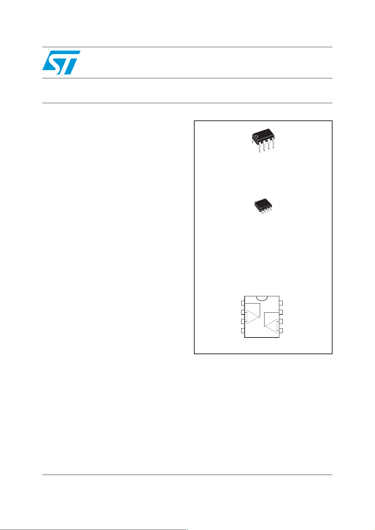
LS204
N
DIP8
(Plastic package)
D
SO-8
(Plastic micro package)
The circuit presents very stable electrical
characteristics over the entire supply voltage
range, and is particularly intended for pr ofessional
and telecom applications (such as active filtering).
Pin connections
(top view)
June 2008 Rev 2 1/16
www.st.com
16
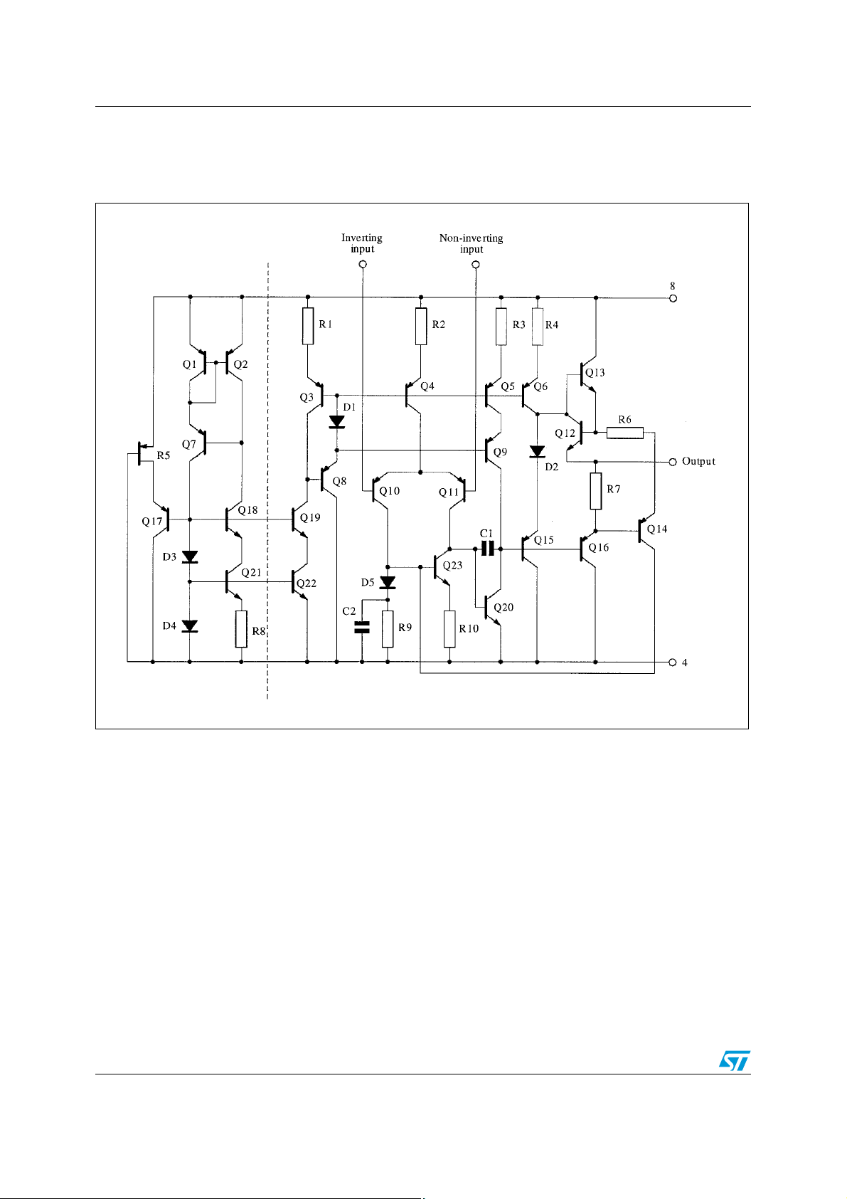
Circuit schematics LS204
1 Circuit schematics
Figure 1. Schematic diagram (1/2 LS204)
2/16
LS204 Absolute maximum ratings and operating conditions
2 Absolute maximum ratings and operating conditions
Table 1. Absolute maximum ratings
Symbol Parameter Value Unit
(2)
(1)
(7)
(3)
(6)
(5)
(8)
(4)
CC
(4)
+
and V
CC
±18 V
±V
CC
V
±(VCC-1) V
125
°C/W
85
40
°C/W
41
Infinite
2kV
200 V
1.5 kV
-
.
V
CC
V
i
V
id
Supply voltage
Input voltage
Differential input voltage
Thermal resistance junction to ambient
R
thja
SO-8
DIP8
Thermal resistance junction to case
R
thjc
SO-8
DIP8
Output short-circuit duration
T
j
T
stg
Junction temperature 150 °C
Storage temperature range -65 to +150 °C
HBM: human body model
ESD
MM: machine model
CDM: charged device model
1. All voltage values, except differential voltage, are with respect to the zero reference level (ground) of the supply voltages
where the zero reference level is the midpoint between V
2. The magnitude of the input voltage must never exceed the magnitude of the supply voltage or 15 volts, whichever is less.
3. Differential voltages are the non-inverting input terminal with respect to the inverting input terminal.
4. Short-circuits can cause excessive heating and destructive dissipation. Values are typical.
5. The output may be shorted to ground or to either supply. Temperature and/or supply voltages must be limited to ensure
that the dissipation rating is not exceeded.
6. Human body model: A 100 pF capacitor is charged to the specified voltage, then discharged through a 1.5 kΩ resistor
between two pins of the device. This is done for all couples of connected pin combinations while the other pins are floating.
7. Machine model: A 200 pF capacitor is charged to the specified voltage, then discharged directly between two pins of the
device with no external series resistor (internal resistor < 5 Ω). This is done for all couples of connected pin combinations
while the other pins are floating.
8. Charged device model: all pins and the package are charged together to the specified voltage and then discharged directly
to the ground through only one pin. This is done for all pins.
Table 2. Operating conditions
Symbol Parameter LS204C LS204I Unit
Supply voltage 6 to 30 V
CC
Common mode input voltage range VDD+1.5 to VCC-1.5 V
icm
Operating free-air temperature range 0 to +70 -40 to +105 °C
3/16
T
V
V
oper
Electrical characteristics LS204
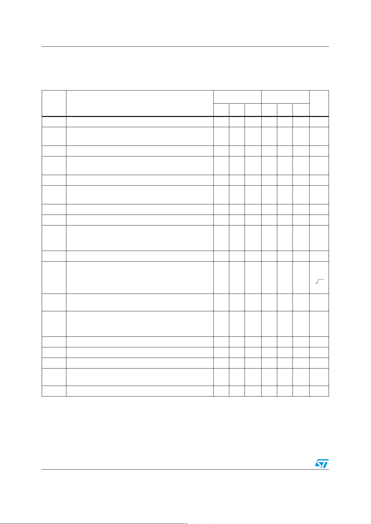
3 Electrical characteristics
Table 3. Electrical characteristics at VCC = ±15 V, T
= +25° C (unless otherwise specified)
amb
LS204I LS204C
Symbol Parameter
Min. Typ. Max. Min. Typ. Max.
Supply current 0.7 1.2 0.8 1.5 mA
I
CC
V
DV
DI
A
Input bias current
I
ib
R
T
< T
amb
< T
max
min
Input resistance (F = 1kHz) 1 1 MΩ
i
Input offset voltage (Rs ≤ 10kΩ)
io
io
I
io
io
I
os
vd
< T
T
min
Input offset voltage drift (Rs ≤ 10kΩ) T
amb
< T
max
min
< T
amb
< T
max
Input offset current
< T
T
min
Input offset current drift T
amb
< T
max
min
< T
amb
< T
max
Output short-circuit current 23 23 mA
Large signal voltage gain T
RL = 2kΩ, V
RL = 2kΩ, V
CC
CC
= ±15V
= ±4V
min
< T
amb
< T
max
50 150
300
0.5 2.5
3.5
100 300
700
0.5 3.5
5
55µV/°C
520
40
12 50
100
0.08 0.1 nA/°C
90 100
95
86 100
95
GBP Gain bandwidth product (F =100kHz) 1.8 3 1.5 2.5 MHz
Equivalent input noise voltage F = 1kHz, Rs = 100Ω
= 50Ω
R
e
n
s
Rs = 1kΩ
Rs = 10kΩ
10
18
8
10
12
20
Unit
nA
mV
nA
dB
nV
----------- Hz
THD
Total harmonic distortion (F = 1kHz, A
Vo= 2Vpp)
= 20dB, RL = 2kΩ,
v
0.03 0.03 %
Output voltage swing
±V
V
= 2kΩ, VCC = ±15V
opp
opp
R
L
= 2kΩ, V
R
L
CC
= ±4V
Large signal voltage swing RL = 10kΩ, F= 10kHz 28 28 V
±13
±3
±13
±3
SR Slew rate (RL = 2kΩ, unity gain) 0.8 1.5 1 V/µs
SVR Supply voltage rejection ratio T
CMR
Common mode rejection ratio V
T
< T
amb
< T
max
min
min
= ±10V
ic
amb
< T
max
90 86 dB
90 86 dB
< T
Vo1/Vo2Channel separation (F= 1 kHz) 100 120 120 dB
4/16
V
pp
LS204 Electrical characteristics
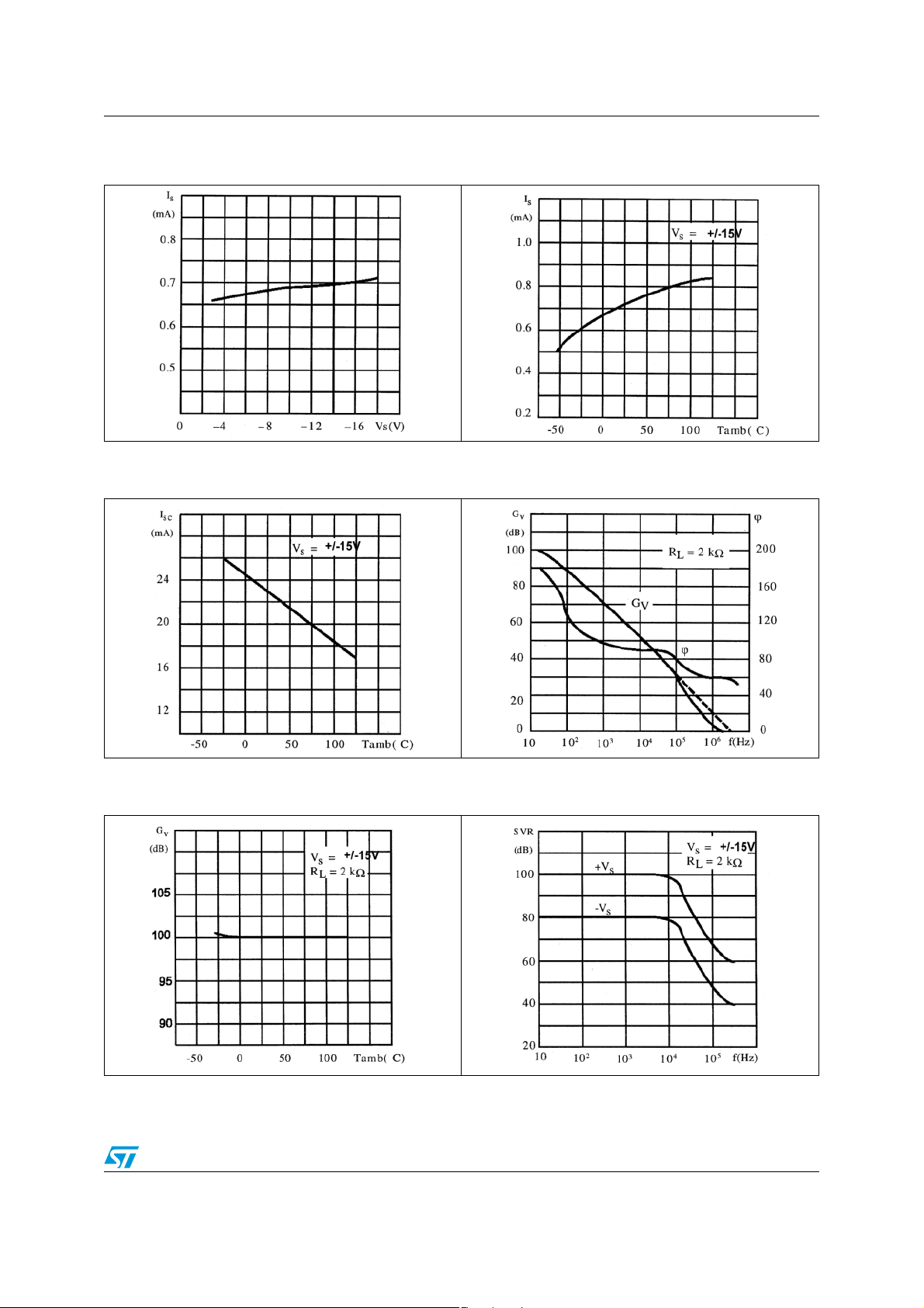
Figure 2. Supply current versus supply
voltage
Figure 4. Output short circuit current versus
ambient temperature
Figure 3. Supply current versus ambient
temperature
Figure 5. Open loop frequency and phase
response
Figure 6. Output loop gain versus ambient
temperature
Figure 7. Supply voltage rejection versus
frequency
5/16

Electrical characteristics LS204
Figure 8. Large signal frequency response Figure 9. Output voltage swing versus load
resistance
Figure 10. Total input noise versus frequency Figure 11. Amplitude response
Figure 12. Amplitude response ( ±1dB ripple)
6/16

LS204 Application information for active low-pass filters
4 Application information for active low-pass filters
4.1 Butterworth
The Butterworth is a "maximally flat" amplitude response filter (Figure 11).
Butterworth filters are used for filtering signals in data acquisition systems to prevent
aliasing errors in samples-data applications and for general purpose low-pass filtering.
The cut-off frequency, Fc, is the frequency at which the amplitude response is down 3 dB.
The attenuation rate be y o nd the cut- off fr equency is n6 dB per octave of frequency, where n
is the order (number of poles) of the filter.
Other characteristics:
● Flattest possible amplitude response
● Excellent gain accuracy at low frequency end of passband
4.2 Bessel
The Bessel is a type of “linear phase” filter.
Because of their linear phase characteristics , these filters appro ximate a consta nt time dela y
over a limited frequency range. Bessel filters pass transient waveforms with a minimum of
distortion. They are also used to provide time delays for low pass filtering of modulated
waveforms and as a “running average” type filter.
The maximum phase shift is radians,
where n is the order (number of poles) of the filter. The cut-off frequency, Fc, is defined as
the frequency at which the phase shift is one half of this value.
For accurate delay, the cut-off frequency should be twice the maximum signal frequency.
Table 4 can be used to obtain the -3 dB frequency of the filter.
Table 4. -3 dB frequency of the filter
-3 dB frequency 0.77 Fc 0.67
Other characteristics:
● Selectivity not as great as Chebyschev or Butterworth
● Very little overshoot response to step inputs
● Fast rise time
4.3 Chebyschev
nπ–
---------2
2 Poles 4 Poles 6 Poles 8 Poles
Fc 0.57 Fc 0.50 Fc
Chebyschev filters have greater selectivity than either Bessel or Butterworth at the expense
of ripple in the passband (Figure 12).
Chebyschev filters are normally designed with peak-to-peak ripple values from 0.2 dB to
2dB.
7/16

Application information for active low-pass filters LS204
Increased ripple in the passband allows increased attenuation above the cut-off frequency.
The cut-off frequency is defined as the frequency at which the amplitude response passes
through the specified maximum ripple band and enters the stop band.
Other characteristics:
● Greater selectivity
● Very non-linear phase resp on se
● High overshoot response to step inputs
Table 5 shows the typical overshoot and setting time response of the low pass filters to a
step input.
Table 5. Overshoot and setting time response of low pass filters to step input
Peak overshoot Settling time (% of final value)
% Overshoot ±1% ±0.1% ±0.01%
4
11
14
14
0.4
0.8
0.6
0.1
11
18
21
23
21
28
32
34
1.1Fc sec.
Fc
1.7/
2.4/Fc
3.1/Fc
Fc
0.8/
1.0/Fc
1.3/Fc
1.6/Fc
Fc
1.1/
3.0/Fc
5.9/Fc
8.4/Fc
Fc
1.6/
4.8/Fc
8.2/Fc
11.6/Fc
1.7Fc sec.
2.8/
3.9S/Fc
5.1/Fc
1.4/Fc
1.8/Fc
2.1/Fc
2.3/Fc
1.6/Fc
5.4/Fc
10.4/Fc
16.4/Fc
2.7/Fc
8.4/Fc
16.3/Fc
24.8/Fc
Fc
1.9Fc sec.
3.8/
5.0S/Fc
7.1/Fc
1.7/Fc
2.4/Fc
2.7/Fc
3.2/Fc
Butterworth
Bessel
Chebyschev (ripple ±0.25dB)
Chebyschev (ripple ±1dB)
Number of
poles
2
4
6
8
2
4
6
8
2
4
6
8
2
4
6
8
4.4 Design of 2nd order active low pass filter (Sallen and Key configuration unity gain op-amp)
Fc
-
-
-
-
-
-
-
For fixed R = R1 = R2, we have (see Figure 13):
1
--- R
1
--- R
ζ
-----ωc
1
-----------
ξ ωc
C1 =
C2 =
8/16

LS204 Application information for active low-pass filters
Figure 13. Filter configuration
C2
R2R1
Vin
C1
Vout
Three parameters are needed to characterize the frequency and phase response of a 2nd
order active filter:
● the gain (Gv),
● the damping factor (ξ ) or the Q factor (Q = 2 ξ )1),
● the cut-off frequency (Fc).
The higher order response is obtained with a series of 2nd order sections. A simple RC
section is introduced when an odd filter is required.
The choice of ξ (or Q factor) determines the filter response (see Table 6).
Table 6. Filter response to ξ or Q factor
Filter response ξ Q Cut-off frequency (Fc)
Bessel Frequency at which phase shift is -90°C
Butterworth Frequency at which Gv = -3 dB
Chebyschev
-------
-------
-------
3
2
2
2
2
2
1
------3
1
------2
Frequency at which the amplitude response passes through
1
-------
specified max. ripple band and enters the stop bank.
2
9/16

Application information for active low-pass filters LS204
4.5 Example
Figure 14. 5th order low-pass filter (Butterworth) with unity gain configuration
C2
Ri
Ci
R2R1
C1
R4R3
C4
C3
In the circuit of Figure 14, for Fc = 3.4 kHz and Ri = R1 = R2 = R3 = 10 kW, we obtain:
1
1
Ci = 1.354
C1 = 0.421
C2 = 1.753
C3 = 0.309
C4 = 3.325
------------ = 6 .33nF
--- -
2π fc
R
1
1
--- -
------------ = 1.97nF
R
2π fc
1
1
--- -
------------ = 8.20nF
R
2π fc
1
1
--- -
------------ = 1.45nF
R
2π fc
1
1
--- -
------------ = 15. 14nF
R
2π fc
The attenuation of the filter is 30 dB at 6.8 kHz and better than 60 dB at 15 kHz.
The same method, referring to Table 7 and Figure 15 is used to design high-pass filters.
In this case the damping factor is found by taking the reciprocal of the num bers in Table 7.
For Fc = 5 kHz and Ci = C1 = C2 = C3 = 1 nF we obtain:
1
1
Ri =
R1 =
R2 =
R3 =
R4 =
-------------- -
0.354
1
-------------- -
0.421
1
-------------- -
1.753
-------------- -
0.309
-------------- -
3.325
--- C
1
--- C
1
--- C
1
1
--- C
1
1
--- C
1
------------ = 2 5. 5k Ω
2π fc
1
------------ = 75.6kΩ
2π fc
1
------------ = 18.2kΩ
2π fc
1
------------ = 103kΩ
2π fc
1
------------ = 9.6kΩ
2π fc
Figure 15. 5th order high-pass filter (Butterworth) with unity gain configuration
R2
Ci
Ri
C1
C2
R1
10/16
C3
C4
R4
R3

LS204 Application information for active low-pass filters
Table 7. Damping factor for low-pass Butterworth filter s
Order CiC1C2C3C4C5C6C7C8
2 0.707 1.41
3 1.392 0.202 3.54
4 0.92 1.08 0.38 2.61
5 1.354 0.421 1.75 0.309 3.235
6 0.966 1.035 0.707 1.414 0.259 3.86
7 1.336 0.488 1.53 0.623 1.604 0.222 4.49
8 0.98 1.02 0.83 1.20 0.556 1.80 0.195 5.125
11/16

Package information LS204
5 Package information
In order to meet environmental requirements, STMicroelectronics offers these devices in
ECOPACK
category of second level interconnect is marke d on the pa ckage and on the inner box label,
in compliance with JEDEC Standard JESD97. The maximum ratings related t o soldering
conditions are also marked on the inner box label. ECOPACK is an STMicroelectronics
trademark. ECOPACK specifications are available at: www.st.com
®
packages. These packages have a lead-free second level interconnect. The
.
12/16

LS204 Package information
5.1 DIP8 package information
Figure 16. DIP8 package mechanical drawing
Table 8. DIP8 package mechanical data
Dimensions
Ref.
Min. Typ. Max. Min. Typ. Max.
A5.330.210
A1 0.38 0.015
A2 2.92 3.30 4.95 0.115 0.130 0.195
b 0.36 0.46 0.56 0.014 0.018 0.022
b2 1.14 1.52 1.78 0.045 0.060 0.070
c 0.20 0.25 0.36 0.008 0.010 0.014
D 9.02 9.27 10.16 0.355 0.365 0.400
E 7.62 7.87 8.26 0.300 0.310 0.325
E1 6.10 6.35 7.11 0.240 0.250 0.280
e 2.54 0.100
eA 7.62 0.300
eB 10.92 0.430
L 2.92 3.30 3.81 0.115 0.130 0.150
Millimeters Inches
13/16

Package information LS204
5.2 SO-8 package information
Figure 17. SO-8 package mechanical drawing
Table 9. SO-8 package mechanical data
Dimensions
Ref.
Min. Typ. Max. Min. Typ. Max.
A1.750.069
A1 0.10 0.25 0.004 0.010
A2 1.25 0.049
b 0.28 0.48 0.011 0.019
c 0.17 0.23 0.007 0.010
D 4.80 4.90 5.00 0.189 0.193 0.197
E 5.80 6.00 6.20 0.228 0.236 0.244
E1 3.80 3.90 4.00 0.150 0.154 0.157
e 1.27 0.050
h 0.25 0.50 0.010 0.020
L 0.40 1.27 0.016 0.050
k1°8°1°8°
ccc 0.10 0.004
Millimeters Inches
14/16

LS204 Ordering information
6 Ordering information
Table 10. Order codes
Order code
Temperature
range
LS204CN
LS204CD
0°C, +70°C
LS204CDT
LS204IN
LS204ID
LS204IDT
LS204IYD
LS204IYDT
1. Qualification and characterization according to AEC Q100 and Q003 or equivalent, advanced screening
(1)
(1)
according to AEC Q001 & Q 002 or equivalent are on-going.
-40°C, +105°C
7 Revision history
Table 11. Document revision history
Date Revision Changes
29-Nov-2001 1 Initial release.
4-Jun-2008 2
Package Packing Marking
DIP8 Tape LS204CN
SO-8
DIP8 Tape LS204IBN
SO-8
SO-8
(Automotive grade)
Updated document format.
Added automotive grade order codes.
Tape or
Tape & reel
Tape or
Tape & reel
Tape or
Tape & reel
204C
204I
204IYD
15/16

LS204
Please Read Carefully:
Information in this document is provided solely in connection with ST products. STMicroelectronics NV and its subsidiaries (“ST”) reserve the
right to make changes, corrections, modifications or improvements, to this document, and the products and services described herein at any
time, without notice.
All ST products are sold pursuant to ST’s terms and conditions of sale.
Purchasers are solely res ponsibl e fo r the c hoic e, se lecti on an d use o f the S T prod ucts and s ervi ces d escr ibed he rein , and ST as sumes no
liability whatsoever relati ng to the choice, selection or use of the ST products and services described herein.
No license, express or implied, by estoppel or otherwise, to any intellectual property rights is granted under this document. If any part of this
document refers to any third pa rty p ro duc ts or se rv ices it sh all n ot be deem ed a lice ns e gr ant by ST fo r t he use of su ch thi r d party products
or services, or any intellectua l property c ontained the rein or consi dered as a warr anty coverin g the use in any manner whats oever of suc h
third party products or servi ces or any intellectual property contained therein.
UNLESS OTHERWISE SET FORTH IN ST’S TERMS AND CONDITIONS OF SALE ST DISCLAIMS ANY EXPRESS OR IMPLIED
WARRANTY WITH RESPECT TO THE USE AND/OR SALE OF ST PRODUCTS INCLUDING WITHOUT LIMITATION IMPLIED
WARRANTIES OF MERCHANTABILITY, FITNESS FOR A PARTICUL AR PURPOS E (AND THEIR EQUIVALE NTS UNDER THE LAWS
OF ANY JURISDICTION), OR INFRINGEMENT OF ANY PATENT, COPYRIGHT OR OTHER INTELLECTUAL PROPERTY RIGHT.
UNLESS EXPRESSLY APPROVED IN WRITING BY AN AUTHORIZED ST REPRESENTATIVE, ST PRODUCTS ARE NOT
RECOMMENDED, AUTHORIZED OR WARRANTED FOR USE IN MILITARY, AIR CRAFT, SPACE, LIFE SAVING, OR LIFE SUSTAINING
APPLICATIONS, NOR IN PRODUCTS OR SYSTEMS WHERE FAILURE OR MALFUNCTION MAY RESULT IN PERSONAL INJ URY,
DEATH, OR SEVERE PROPERTY OR ENVIRONMENTAL DAMAGE. ST PRODUCTS WHICH ARE NOT SPECIFIED AS "AUTOMOTIVE
GRADE" MAY ONLY BE USED IN AUTOMOTIVE APPLICATIONS AT USER’S OWN RISK.
Resale of ST products with provisions different from the statements and/or technical features set forth in this document shall immediately void
any warranty granted by ST fo r the ST pro duct or serv ice describe d herein and shall not cr eate or exten d in any manne r whatsoever , any
liability of ST.
ST and the ST logo are trademarks or registered trademarks of ST in vari ous countries.
Information in this document su persedes and replaces all information previously supplied.
The ST logo is a registered trademark of STMicroelectronics. All other names are the property of their respective owners.
© 2008 STMicroelectronics - All rights reserved
STMicroelectronics group of compan ie s
Australia - Belgium - Brazil - Canada - China - Czech Republic - Finland - Fran ce - Germany - Hong Kong - India - Israel - Italy - Japan -
Malaysia - Malta - Morocco - Singapore - Spain - Sweden - Switzerland - United Kingdom - United States of America
www.st.com
16/16
 Loading...