

Page 1

AN4450
Application note
Hardware and software guidelines for use of LPS25H pressure
sensor
By Raffaele Di Vaio
Introduction
The LPS25H is an ultra-compact absolute piezoresistive pressure sensor with enhanced
digital features in a small package footprint.
Unless specifically noted, all recommendations in this document apply only to the LPS25H.
Please refer to the LPS25H datasheet (available at www.st.com) for device and feature
definitions.
April 2014 DocID025978 Rev 1 1/26
www.st.com
Page 2

Contents AN4450
Contents
1 Pressure sensor evaluation boards . . . . . . . . . . . . . . . . . . . . . . . . . . . . 4
2 Hardware (designing PCB schematics and layout) . . . . . . . . . . . . . . . . 6
2.1 LPS25H device package, interconnect and polarization . . . . . . . . . . . . . . 6
2.1.1 Package drawings . . . . . . . . . . . . . . . . . . . . . . . . . . . . . . . . . . . . . . . . . . 6
2.1.2 Pin mapping . . . . . . . . . . . . . . . . . . . . . . . . . . . . . . . . . . . . . . . . . . . . . . . 7
2.1.3 Typical application circuit . . . . . . . . . . . . . . . . . . . . . . . . . . . . . . . . . . . . . 8
2.2 Pressure sensor PCB layout and soldering recommendations . . . . . . . . . 9
2.2.1 PCB design rules . . . . . . . . . . . . . . . . . . . . . . . . . . . . . . . . . . . . . . . . . . . 9
2.2.2 Stencil design and solder paste application . . . . . . . . . . . . . . . . . . . . . . 10
2.2.3 Process consideration . . . . . . . . . . . . . . . . . . . . . . . . . . . . . . . . . . . . . . 10
2.2.4 Manual soldering . . . . . . . . . . . . . . . . . . . . . . . . . . . . . . . . . . . . . . . . . . 11
3 Power supply: consumption estimation and optimization . . . . . . . . . 12
3.1 Common rules for low power consumption . . . . . . . . . . . . . . . . . . . . . . . 14
4 Using the device step-by-step, from basic to advanced . . . . . . . . . . . 15
4.1 First time bring-up (I²C example) . . . . . . . . . . . . . . . . . . . . . . . . . . . . . . . 15
4.2 Quick troubleshooting guide . . . . . . . . . . . . . . . . . . . . . . . . . . . . . . . . . . . 15
4.3 One-shot mode measurement sequence . . . . . . . . . . . . . . . . . . . . . . . . . 16
5 Using FIFO modes . . . . . . . . . . . . . . . . . . . . . . . . . . . . . . . . . . . . . . . . . . 17
5.1 Effective use of the FIFO . . . . . . . . . . . . . . . . . . . . . . . . . . . . . . . . . . . . . 17
5.1.1 Accessing the FIFO data . . . . . . . . . . . . . . . . . . . . . . . . . . . . . . . . . . . . 17
5.1.2 Bypass mode (F_MODE[2..0]="000" in FIFO_CTRL (0x2E)) . . . . . . . . 18
5.1.3 FIFO mode (F_MODE[2..0]="001" in FIFO_CTRL (0x2E)) . . . . . . . . . . 18
5.1.4 Stream mode (F_MODE[2..0]="010" in FIFO_CTRL (0x2E)) . . . . . . . . 18
5.1.5 FIFO mean mode (F_MODE[2..0]="110" in FIFO_CTRL (0x2E)) . . . . . 18
5.1.6 Hardware digital filter . . . . . . . . . . . . . . . . . . . . . . . . . . . . . . . . . . . . . . . 19
5.2 Extra FIFO modes . . . . . . . . . . . . . . . . . . . . . . . . . . . . . . . . . . . . . . . . . . 20
5.2.1 Stream to FIFO mode (F_MODE[2..0]="011" in FIFO_CTRL (0x2E)) . . 20
5.2.2 Bypass to Stream mode (F_MODE[2..0]="100" in FIFO_CTRL (0x2E)) 20
5.2.3 Bypass to FIFO mode (F_MODE[2..0]="111" in FIFO_CTRL (0x2E)) . . 21
2/26 DocID025978 Rev 1
Page 3

AN4450 Contents
6 Software . . . . . . . . . . . . . . . . . . . . . . . . . . . . . . . . . . . . . . . . . . . . . . . . . . 22
6.1 Hints . . . . . . . . . . . . . . . . . . . . . . . . . . . . . . . . . . . . . . . . . . . . . . . . . . . . . 22
6.2 One-shot mode conversion time estimation . . . . . . . . . . . . . . . . . . . . . . . 22
6.3 Reference SW to get started with LPS25H . . . . . . . . . . . . . . . . . . . . . . . 22
6.4 Pressure to altitude conversion . . . . . . . . . . . . . . . . . . . . . . . . . . . . . . . . 22
6.5 SW filtering & internal FIFO . . . . . . . . . . . . . . . . . . . . . . . . . . . . . . . . . . . 23
6.6 Reset the device to power-on configuration . . . . . . . . . . . . . . . . . . . . . . . 23
6.7 Absolute accuracy drift due to soldering . . . . . . . . . . . . . . . . . . . . . . . . . 24
6.7.1 Correcting soldering drift (one-point calibration) . . . . . . . . . . . . . . . . . . 24
7 Revision history . . . . . . . . . . . . . . . . . . . . . . . . . . . . . . . . . . . . . . . . . . . 25
DocID025978 Rev 1 3/26
26
Page 4
Pressure sensor evaluation boards AN4450
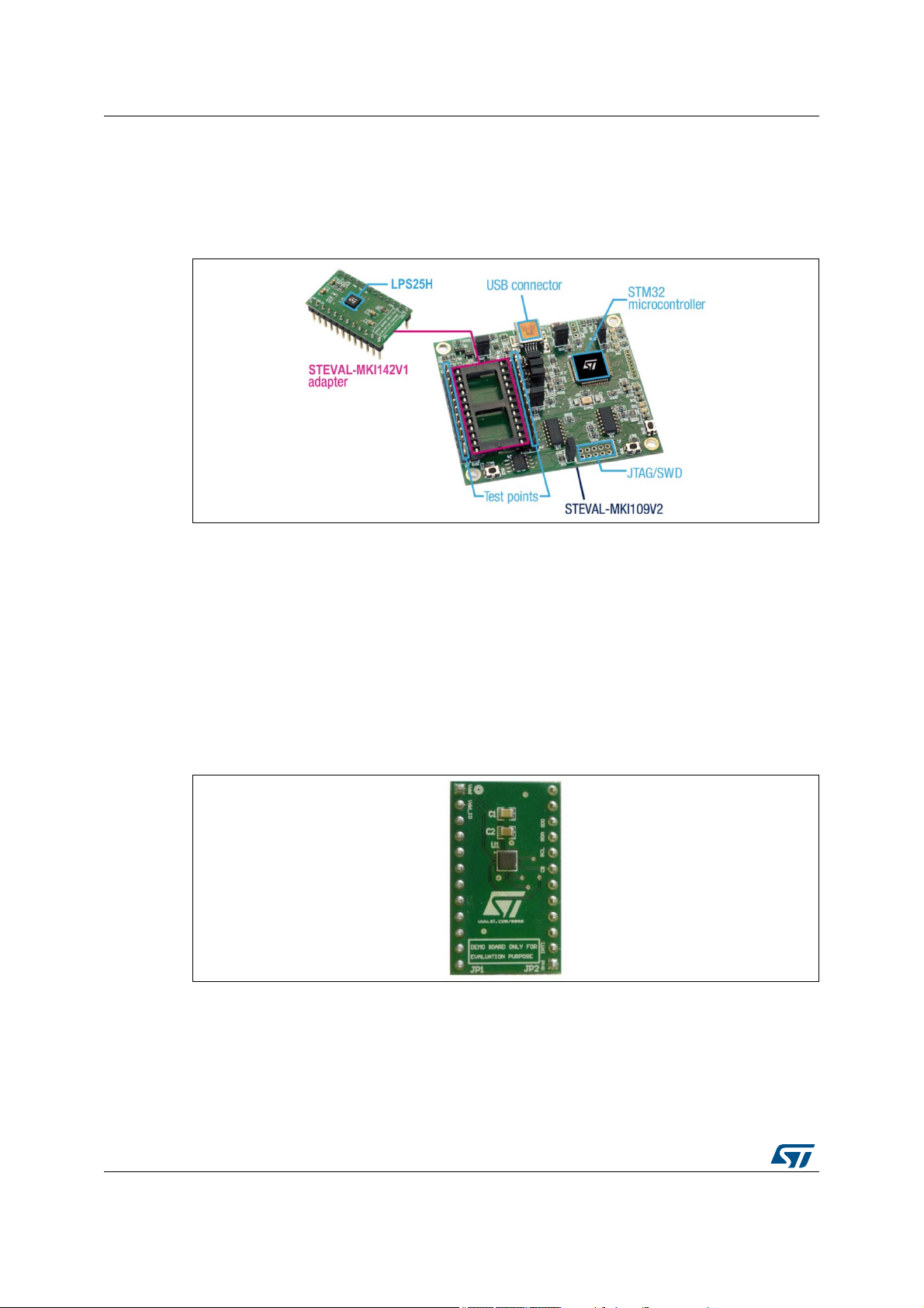
1 Pressure sensor evaluation boards
UNICO/eMotion evaluation system: [STEVAL-MKI109V2] + [STEVAL-MKI142V1 or V2].
Figure 1. STEVAL-MKI142V1 LPS25H adapter, STEVAL-MKI109V2 MEMS motherboard
The STEVAL-MKI109V2 is a motherboard designed to provide users with a complete,
ready-to-use platform for the demonstration of STMicroelectronics MEMS products. The
board features a DIL 24 socket to mount all available adapters for both digital and analog
output MEMS devices.
The motherboard includes a high-performance 32-bit microcontroller, which functions as a
bridge between the sensor and a PC, on which it is possible to use the downloadable
graphical user interface (GUI) from ST (Unico SW), or dedicated software routines for
customized applications.
A plain terminal (such as MS windows hyper-terminal (C)) can also be used to access the
sensor registers by text read/write commands.
Figure 2. STEVAL-MKI142V1 - LPS25H adapter
The STEVAL-MKI142V1 adapter board is designed to facilitate the demonstration of the
LPS25H product. The board offers an effective solution for fast system prototyping and
device evaluation directly within the user’s own application.
The STEVAL-MKI142V1 can be plugged into a standard DIL 24 socket. The adapter
provides the complete LPS25H pin-out and comes ready-to-use with the recommended
decoupling capacitors on the VDD power supply line. No pull-ups are provided.
4/26 DocID025978 Rev 1
Page 5

AN4450 Pressure sensor evaluation boards
The STEVAL-MKI109V2 MEMS (aka eMotion board, shipped with pre-loaded eMotion FW)
is completed by a MS Windows™-based SW application called Unico. This tool may be
used as a simple real-time demonstrator or to verify device performance.
It also allows easy monitoring of the register status and allows changes to them based on
the intended scenario.
Recommended FW/SW revisions fully supporting the STEVAL-MKI142V1 are:
eMotion V3.0.6
Unico Rev. 3.0.1.0 beta
or newer.
DocID025978 Rev 1 5/26
26
Page 6
Hardware (designing PCB schematics and layout) AN4450
2 Hardware (designing PCB schematics and layout)
2.1 LPS25H device package, interconnect and polarization
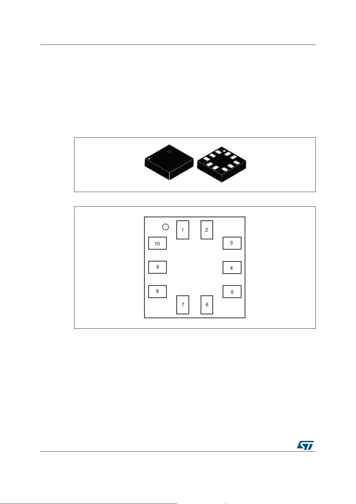
2.1.1 Package drawings
Pressure sensor LPS25H is available in a holed LGA package: HCLGA-10L (1mm
thickness).
Figure 3. HCLGA-10L 2.5x2.5x1.0 mm
Figure 4. Pin mapping (bottom view)
6/26 DocID025978 Rev 1
Page 7

AN4450 Hardware (designing PCB schematics and layout)
2.1.2 Pin mapping
Table 1. LPS25H pin mapping details
Pin # Name Function What to do
1 VDD_IO Power supply for I/O pins I/O supply voltage (1.7V ~ 3.6V)
2
3 Reserved Reserved Connect to PCB ground
4
5
6CS
7 INT1 Interrupt 1 (or data ready) Leave unconnected if unused
8 GND_IO I/O pins ground Connect to PCB ground
9 GND Ground Connect to PCB ground
10 VDD Power supply Supply voltage (1.7V ~ 3.6V)
SCL
SPC
SDA
SDI
SDIO
SA0
SDO
I²C serial clock (SCL)
SPI serial port clock (SPC)
I²C serial data (SDA)
4-wire SPI serial data input (SDI)
3-wire SPI serial data input/output (SDIO)
I²C slave address select (SA0)
4-wire SPI serial data output (SDO)
I²C/SPI mode selection
SPI chip select
Optional pull-up resistor, connected to VDD_IO,
could be required for I²C (see I²C standard for
recommended value)
Optional pull-up resistor, connected to VDD_IO,
could be required for I²C (see I²C standard for
recommended value)
SA0=1: 0xBA/BB I²C slave address + R/W
SA0=0: 0xB8/B9 I²C slave address + R/W
CS=1: I²C mode
CS=ChipSelect in SPI mode
DocID025978 Rev 1 7/26
26
Page 8
Hardware (designing PCB schematics and layout) AN4450
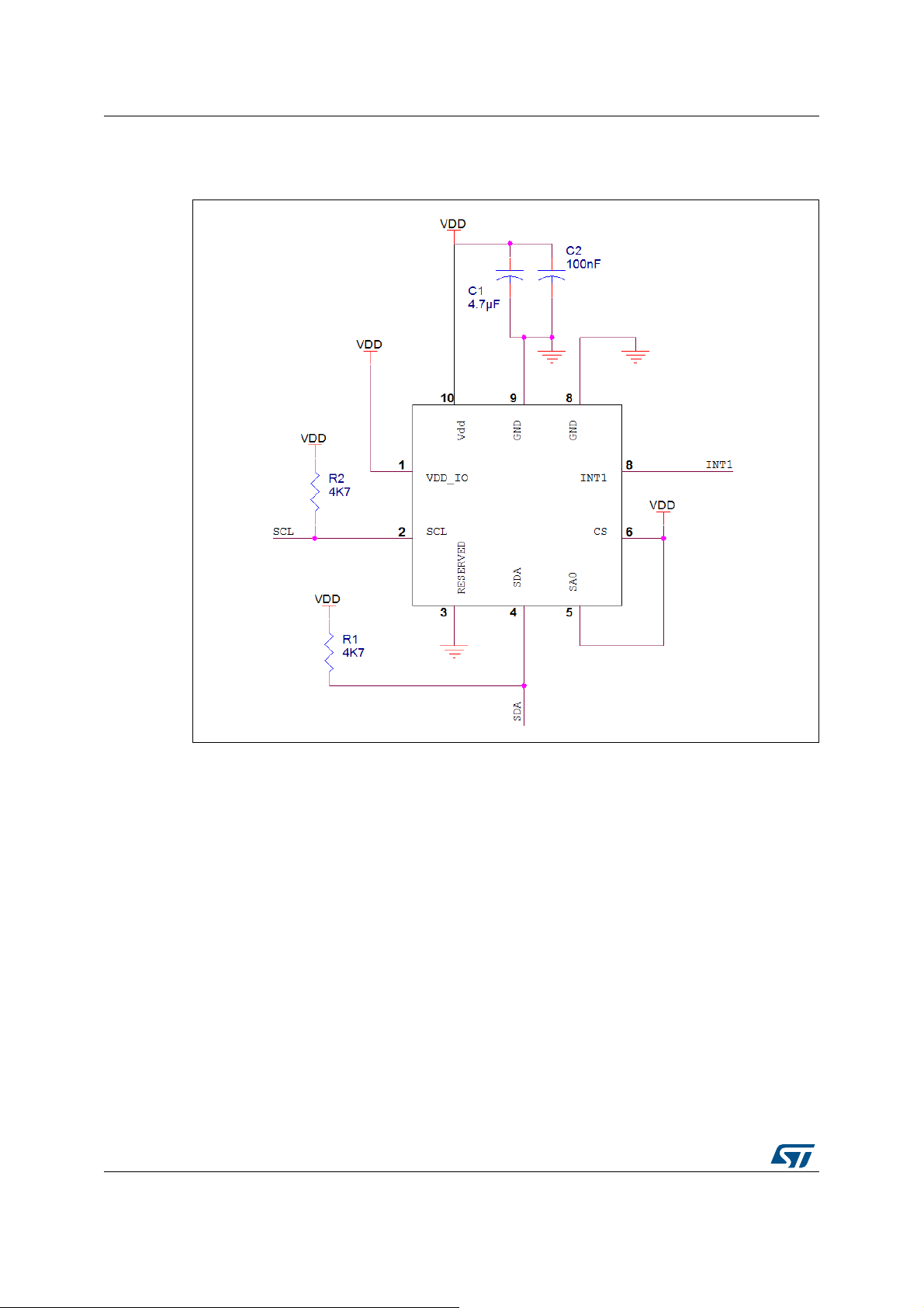
2.1.3 Typical application circuit
Figure 5. LPS25H electrical connection (I²C communication example w/SA0=1)
Key notes:
The device core is supplied through the VDD line. Power supply decoupling capacitors
(100 nF and at least 4.7 µF) must be placed as near as possible to the supply pads of the
device.
VDD_IO should match the one requested by the host controller. In any case VDD_IO must
be the same or lower than VDD. In the example shown here, VDD_IO is connected to VDD.
Please note that the LPS25H does not have an internal pull-up on the I²C lines (SCL and
SDA). They must be added externally according to the I²C bus speed and load, and
connected to VDD_IO.
In I²C mode, SA0 =1 (pin directly connected to VDD_IO) sets the slave address to 0xBA for
write and 0xBB for read. A pull-up resistor could be a better choice if there is a need to
communicate alternatively in I²C or SPI 4-wires, since pin 5 is SDO for SPI 4-wires and of
course it cannot function if hard-connected to VDD_IO.
The I²C interface is compliant with fast mode (400 kHz) I²C standards as well as with normal
mode.
8/26 DocID025978 Rev 1
Page 9

AN4450 Hardware (designing PCB schematics and layout)
In SPI the CS pin is the chip select and it is controlled by SPI master. It goes low at the start
of the communication and returns high at the end.
SPI communication can work in 2 different modes: 3-wires and 4-wires. In the first case the
pins used are: CS, SPC and SDIO; in the latter: CS, SPC, SDI and SDO. SPI mode
selection is done through bit 0 of register CTRL_REG1: 0=4-wires; 1=3-wires.
Both SPI and I²C interfaces are active by default. In case of SPI use only, I²C interface can
optionally be disabled by programming the corresponding bit in a control register
(CTRL_REG2[3]=1).
2.2 Pressure sensor PCB layout and soldering recommendations
The LPS25H has an aperture on top of the package, so special care is required since
sensor performance could be compromised by:
Mechanical stress coming from the PCB board
– The whole package surface + air should have minimum temperature gradient
– Avoid placement in long and narrow PCB area, warp-free area
Temperature gradients (non-uniform/rapidly changing temperature around sensor)
Strong electrical field / light source
Localized air pressure stability (unwanted fast air pressure variation, fans)
Dust and water exposure/condensation (GORE-TEX
The HCLGA package is compliant with the ECOPACK
soldering heat resistance according to JEDEC J-STD-020.
®
protection, etc.)
®
standard and is qualified for
2.2.1 PCB design rules
The pressure sensor is affected by mechanical stress coming from the PCB board, hence it
should be minimized. A typical suggestion is to place the pressure sensor at the edge of the
PCB where warping is minimal.
PCB land and solder masking general recommendations are shown below. Refer to the
LPS25H datasheet for pad count, size and pitch.
It is recommended to open a solder mask external to PCB land.
The area below the sensor (on the same side of the board) must be defined as a keep-
out area. It is strongly recommended not to place any structure on the top metal layer
underneath the sensor.
This means that it is possible to place the ground plane in the PCB middle layer under
the LPS25H, but not in the plane immediately under the LPS25H.
Traces connected to pads should be as symmetrical as possible. Symmetry and
balance for pad connection will help component self-alignment and will lead to better
control of solder paste reduction after reflow.
For better performance over temperature, it is strongly recommended not to place large
insertion components like buttons or shielding boxes at distances less than 2 mm from
the sensor.
The pin 1 indicator must be left unconnected to ensure proper device operation.
DocID025978 Rev 1 9/26
26
Page 10

Hardware (designing PCB schematics and layout) AN4450
Figure 6. Recommended land and solder mask design for *LGA packages
A = Clearance from PCB land edge to solder mask opening
solder mask is opened externally to device area
B = PCB land length = *LGA solder pad length + 0.1 mm
C = land width = *LGA solder pad width + 0.1 mm
D = Solder mask opening length = PCB land length + 0.3 mm: design 0.05 mm inside
and 0.25 mm outside
E = Solder mask opening width = PCB land width + 0.1 mm
2.2.2 Stencil design and solder paste application
The soldering paste thickness and pattern are important for a proper pressure sensor
mounting process.
Stainless steel stencils are recommended
Stencil thickness of 90 - 150 µm (3.5 - 6 mils) is recommended for screen printing
The final soldering paste thickness should allow proper cleaning of flux residues and
clearance between sensor package and PCB
Stencil aperture should have a rectangular shape with dimensions up to 25 µm (1 mil)
smaller than PCB land
The openings of the stencil for the signal pads should be between 70 - 80% of the PCB
pad area
Optionally, for better solder paste release, the aperture walls should be trapezoidal and
the corners rounded
The fine IC leads pitch requires accurate alignment of the stencil to the PCB. The
stencil and printed circuit assembly should be aligned to within 25 µm (1 mil) prior to
application of the solder paste
≥ 0.25 mm to ensure that
2.2.3 Process consideration
In using non self-cleaning solder paste, proper board washing after soldering must be
carried out to remove any possible sources of leakage between pads due to flux residues.
However, take care not to perform the cleaning process on top of the pressure sensor.
10/26 DocID025978 Rev 1
Page 11

AN4450 Hardware (designing PCB schematics and layout)
The PCB soldering profile depends on the number, size and placement of components on
the board. The soldering profile should be defined by experience, rather than the pressure
sensor soldering profile only.
The JEDEC reflow profile is provided below.
Figure 7. High temperature lead-free soldering profile 260 °C max
No solder material reflow on the side of the package is allowed since *LGA packages show
metal trace out of package side.
No need to use any tape to cover the hole on the CAP of the LPS25H during reflow. The
cleaning of the PCB is not a general task, as it should be cleaned only when the PCB is
contaminated during reflow. ST does not ship the LPS25H covered.
2.2.4 Manual soldering
Apply solder paste (e.g. ALPHA® OM-338-T) on the PCB solder pads using a syringe (air,
bubble free), and position the *LGA accordingly. Then press it to ensure it is flat on the PCB,
and heat it in an oven using the 260 °C JDEC profile (the one shown in Figure 7 ).
Take care that hand soldering is within spec. In any case, in an emergency situation, coat
the solder pad with tin-lead, and use solder wick to flatten the solder ball. Then put the
soldering iron on the *LGA land marks to deposit solder on the *LGA pads. Then position it,
and use a hot air gun to melt both sides and obtain eutectic bonding (350 °C). However, this
is not recommended. Hot air from the gun must be spread around the package dynamically;
keep moving the air gun around the *LGA.
Solder heat resistance and environmental specification
The second level interconnect category on ST ECOPACK® lead-free package is marked on
the inner box label, in compliance with JEDEC standard JESD97. Soldering condition
maximum ratings are also marked on the same label.
HCLGA/HLGA packages for pressure sensors are qualified for soldering heat resistance
according to JEDEC J-STD-020, in MSL3 condition.
DocID025978 Rev 1 11/26
26
Page 12

Power supply: consumption estimation and optimization AN4450
3 Power supply: consumption estimation and
optimization
There are 2 supply voltages in the LPS25H: VDD and VDD_IO.
VDD is the core voltage used to supply to the internal circuits, power on reset, and the
sensor.
VDD_IO is the supply for the I
In order to prevent possible leakage in the operational condition, it is necessary to ensure
VDD_IO <= VDD.
The operating voltage for both VDD_IO and VDD is 1.7 V to 3.6 V.
The LPS25H can also be powered directly by a small lithium coin battery like the CR2032.
This type of battery has a current capability of 220 mAh, enough to sustain the sensor peak
current (less than 1 mA).
Provided that the battery fluctuation, which could be in the range of 0.4 V, is within the
“normal operating voltage conditions” (even with an aged battery) and the recommended
decoupling capacitors are placed near the sensor, our tests with batteries and switched
resistive loads show that the sensor functions correctly even with fast slew rates.
2
C / SPI blocks and interface signals.
During the main power-on transition, the system will initialize the internal registers according
to the factory-stored information (such as sensor calibration data).
This is triggered by VDD increasing above 1.6 V.
Current consumption during the device initialization peaks around 200 µA (for a duration of
about 600 µs).
After these steps, the LPS25H will enter a power-down state. The LPS25H is ready in
power-down from power-off in about 2.5 ms.
The LPS25H runs in normal mode from power-down state (toggling PD bit[7] in
CTRL_REG1, 0x20) in a few microseconds. Depending on register RES_CONF (0x10)
settings, the first valid measurement is ready after about 2 ms (minimum resolution, with
AVGT[1:0]=00; AVGP[1:0]=00, i.e. 8+8 samples) or about 37 ms (maximum resolution, with
AVGT[1:0]=11; AVGP[1:0]=11, i.e. 64+512 samples).
The typical conversion time (with +/-3% accuracy at room temperature) is given by the
formula:
Equation 1
Tconversion in µs = 62 * (Tavg + Pavg) + 975
where Tavg and Pavg are the values, respectively, for temperature and for pressure
measurements, selected in register RES_CONF as the number of averaged samples per
measurement.
– Example: Tavg = 64; Pavg = 512; Typ. conversion time 36687 µs
The LPS25H has been designed to have a very low power consumption. The majority of the
internal blocks are switched-on only during the acquisition time. In one-shot mode the
device automatically goes into standby when the measurement is completed.
The minimum power consumption occurs when the device is in power-down (PD=0 bit[7] of
the CTRL_REG1 (0x20)) AND the interrupt pin is not configured to drain current. In normal
12/26 DocID025978 Rev 1
Page 13

AN4450 Power supply: consumption estimation and optimization
operating mode the power consumption depends on HW-averaging (resolution) and output
data rate (auto-refresh frequency) settings. The following formula gives an indication of the
current consumption in relation to average and ODR. This can be used to find the best
compromise, for a given application, between consumption, update speed and filtering.
Equation 2
Idd = [(3uA/Hz +42nA/Hz*Pavg) + 30nA/Hz*Tavg]*ODR
where:
Pavg = value set by AVGP[1:0] (8, 32, 128, 512)
Tavg = value set by AVGT[1:0] (8,16, 32, 64)
ODR = rates according to ODR[2:0] (1, 7, 12.5, 25Hz)
Table 2. ODR, AVGT and AVGP correspondence
ODR[6..4]@0x20 ODR AVGT[3..2]@0x10 Tavg AVGP[1..0]@0 x10 Pavg
11Hz 0 8 0 8
27Hz 1 16 1 32
3 12.5Hz 2 32 2 128
4 25Hz 3 64 3 512
a) Example 1:
– ODR= 25 Hz
– Pavg= pressure average=512
– Tavg= temperature average=64
– Idd= 661 µA (Vdd independent at first approximation)
b) Example 2:
– ODR=1 Hz
– Pavg= pressure average=512
– Tavg= temperature average=64
– Idd= 26.4 µA
c) Example 3:
– ODR= 1 Hz
– Pavg= pressure average=8
– Tavg= temperature average=8
– Idd= 3.6 µA
In order to improve system power saving, the LPS25H embeds a FIFO buffer capable of
storing up to 32 pressure output values. Since the host processor does not need to
continuously poll data from the sensor, it can wake up (on programmable interrupt from the
sensor) only when requested and burst the significant data out from the buffer.
The FIFO can alternatively be configured as moving average to reduce the noise figure (or
to reduce the ODR rate while keeping the same noise figure, traded for delay).
DocID025978 Rev 1 13/26
26
Page 14

Power supply: consumption estimation and optimization AN4450
3.1 Common rules for low power consumption
Here are some notes about possible sources of power leakage:
– Do not leave any input pin un-terminated (floating). This may leave the internal
circuit in undefined state, creating/introducing extra power consumption. Connect
unused input pins (such as CS, and SA0 if a single sensor is used on the I
to VDD_IO. Use a pull-up resistor where needed.
– Do not connect a push-pull output pin directly to GND or VDD_IO (unless it can be
ensured that no change on that pin status will be made by SW).
– Select the proper I
2
C pull-up resistor (to VDD_IO) according to the bus load and
working frequency.
2
C bus)
14/26 DocID025978 Rev 1
Page 15

AN4450 Using the device step-by-step, from basic to advanced
4 Using the device step-by-step, from basic to
advanced
4.1 First time bring-up (I²C example)
1. Start by using the same supply for VDD_IO and VDD to check device functionality.
2. Check supply impedances and ensure that all the pins voltages are in static condition.
3. The device is a slave with 1 byte sub-address which MSB should be ‘1’ to enable the
multiple data read/write at increasing addresses (bit 7 = 1 enables I²C sub-address
multi-byte auto-increment)
4. Use a normal I²C bus speed (<400 kHz)
5. Read the chip ID byte (sub address 0x0F, or 0x8F in case of auto-increment option):
0xBD should be read
4.2 Quick troubleshooting guide
If the device is not communicating properly on the I²C bus:
1. If the I²C slave address is not acknowledged, check:
– Power supply is present and matches the I²C master VDD_IO
– I²C line pull-ups are present and with the correct values
– The slave address is correctly selected
– There are no other slaves with same address on the I²C bus lines.
– Make sure the maximum I²C speed is driven by the slowest slave on the same I²C
bus.
– Use an oscilloscope to check that the device acknowledges its slave address.
2. If the device responds and the pressure is always fixed and out of range (e.g. 760 mb),
make sure that AVGT and AVGP are in line with the specs and wait for the data ready
bit flag before reading the pressure registers.
3. If the device is reporting a value with a small offset compared to the expected one, a
single point calibration may be needed in order to compensate the post soldering
package stress (see Section 6.7)
DocID025978 Rev 1 15/26
26
Page 16

Using the device step-by-step, from basic to advanced AN4450
4.3 One-shot mode measurement sequence
1. Power down the device (clean start)
– WriteByte(CTRL_REG1_ADDR = 0x00); // @0x20=0x00
2. Turn on the pressure sensor analog front end in single shot mode
– WriteByte(CTRL_REG1_ADDR = 0x84); // @0x20=0x84
3. Run one-shot measurement (temperature and pressure), the set bit will be reset by the
sensor itself after execution (self-clearing bit)
– WriteByte(CTRL_REG2_ADDR = 0x01); // @0x21=0x01
4. Wait until the measurement is completed
– ReadByte(CTRL_REG2_ADDR = 0x00); // @0x21=0x00
5. Read the temperature measurement (2 bytes to read)
– Read((u8*)pu8, TEMP_OUT_ADDR, 2); // @0x2B(OUT_L)~0x2C(OUT_H)
– Temp_Reg_s16 = ((u16) pu8[1]<<8) | pu8[0]; // make a SIGNED 16 bit variable
– Temperature_DegC = 42.5 + Temp_Reg_s16 / 480; // offset and scale
6. Read the pressure measurement
– Read((u8*)pu8, PRESS_OUT_ADDR, 3); //
@0x28(OUT_XL)~0x29(OUT_L)~0x2A(OUT_H)
– Pressure_Reg_s32 = ((u32)pu8[2]<<16)|((u32)pu8[1]<<8)|pu8[0]; // make a
SIGNED 32 bit
– Pressure_mb = Pressure_Reg_s32 / 4096; // scale
7. Check the temperature and pressure values make sense
– Reading fixed 760 hPa, means the sensing element is damaged.
Example of register measurements and conversion:
P = 0x3FF58D means 4191629 / 4096 = 1023.347 hPa
T = 0xE07C means 42.5 + (-8068/480) = 25.7 °C
{ as reference: 0x6BD0 = 100°C; 0xB050=0 °C }
The value read from the PRESS_OUT registers is always the difference of the sensor
measured pressure (after averaging) and a base value, that can be either the value copied
in the RPDS register (reference pressure after soldering, to correct the pressure offset due
to mechanical stress, 16-bit value corresponding to the MSB part of the pressure value) by
default after power-up, or the value written in the REF_P registers (24-bit value).
To select REF_P as base value, and hence enable differential mode, bit AUTOZERO (bit[1]
of CTRL_REG2, (0x21), which is a self-clearing bit) must be set: the current PRESS_OUT
value is copied into REF_P registers, and from the next available measurement, the
PRESS_OUT value is the difference between the current measure and the “frozen”
reference value. In case the application requires to switch back to default mode, the bit
RESET_AZ (bit[1] of CTRL_REG1 (0x20), which is a self-clearing bit) must be set.
PRESS_OUT is then computed using RPDS registers value as reference.
RPDS_L and RPDS_H calibration values can be written on the volatile memory by the
microcontroller after sensor power-on: the value shall be permanently stored in the
application memory during manufacturing (see Section 6.7).
In special cases, there’s also the possibility to store the RPDS calibration value inside the
LPS25H non-volatile memory.
16/26 DocID025978 Rev 1
Page 17

AN4450 Using FIFO modes
5 Using FIFO modes
5.1 Effective use of the FIFO
The LPS25H embeds a 32-slot x 24 bit FIFO for pressure data coming from the registers
that normally feed PRESS_OUT (@ 0x28/0x29/0x2A). It allows lower frequency of serial
bus transactions and provides more time to collect all measurements taken.
The FIFO buffer is enabled by setting FIFO_EN to 1 (bit[6] in CTRL_REG2) and can work in
4 different main modes: Bypass Mode, FIFO Mode, Stream Mode and FIFO Mean Mode.
Each mode is selected by the 3 FIFO_MODE bits in FIFO_CTRL register.
Watermark level (P1_WTM), FIFO_empty (P1_EMPTY), FIFO_full (P1_Overrun) or
DATA_Ready (P1_DRDY) events can be enabled (in register CTRL_REG4 (0x23)) to
generate dedicated interrupts on the INT1 pin (provided that bit[1:0] of register CTRL_REG3
(0x22) are configured “00” to select Data Signal).
When FIFO is enabled temperature data must be read separately from pressure data. The
temperature readout is always referred to the last pressure data in the FIFO, as no FIFO is
available for temperature data. The register auto-increment “rounding” is then different
depending on FIFO_EN status, as shown in the picture below.
Figure 8. Auto-increment rounding depending on FIFO_EN
To switch FIFO on/off, the bypass mode must be used. Switching the FIFO on/off only using
the FIFO_en bit of register CTRL_REG2 would cause a wrong FIFO behavior.
5.1.1 Accessing the FIFO data
FIFO data is read through PRESS_OUT registers (0x28/0x29/0x2A). When FIFO is in
stream, trigger (i.e. state change on trigger) or FIFO mode, a read operation to the
PRESS_OUT registers provides the data stored in the FIFO. When in FIFO mean mode it is
not possible to read the data in the buffer, only the final averaged value will be available in
PRESS_OUT registers at the end of the process done with the selected speed (see
Section 5.1.5).
Each time data is read from the FIFO, the oldest entry is placed in the PRESS_OUT
registers and both single read and multiple read operations can be used.
DocID025978 Rev 1 17/26
26
Page 18

Using FIFO modes AN4450
The whole FIFO content can be read by reading 3x32 bytes from PRESS_OUT_XL location
in a single I²C read transaction. Internally the reading address will automatically roll back
from 0x2A down to 0x28 when FIFO is active to allow a quick read of its content.
5.1.2 Bypass mode (F_MODE[2..0]="000" in FIFO_CTRL (0x2E))
The FIFO is not operational and for this reason the buffer remains empty. The pressure
value is sent directly to PRESS_OUT registers.
5.1.3 FIFO mode (F_MODE[2..0]="001" in FIFO_CTRL (0x2E))
The measurement from the sensor are sent to FIFO buffer, the FIFO content is read using
the registers PRESS_OUT_XL (0x28), PRESS_OUT_L (0x29) and PRESS_OUT_H (0x2A).
An interrupt can be enabled (WTM_EN bit[5] in CTRL_REG2 (0x21) in order to be raised
when the FIFO is filled to the level specified by the WTM_POINT[4..0] bits[4..0] in the
FIFO_CTRL (0x2E) register. The FIFO continues filling until it is full (32 slots of data for XL,
L and H). When full, the FIFO stops collecting incoming pressure measurements.
5.1.4 Stream mode (F_MODE[2..0]="010" in FIFO_CTRL (0x2E))
Like in FIFO mode the measurements are stored in the buffer before being available in
PRESS_OUT_XL, PRESS_OUT_L and PRESS_OUT_H. On the contrary of FIFO mode,
when full, the FIFO discards the older data as the new arrive. An interrupt can be enabled
and set as in FIFO mode though the same register FIFO_CTRL (0x2E).
Stream mode can be used to implement a digital filter averaging the samples stored in the
FIFO.
5.1.5 FIFO mean mode (F_MODE[2..0]="110" in FIFO_CTRL (0x2E))
This mode is used in order to enable the “low noise mode”. In this mode the pressure data
are stored in the FIFO after being averaged depending on AVGP[1..0] bit in register
RES_CONF (0x10).
Pressure data stored in the FIFO buffer are further averaged, to implement a moving
average, using a number of samples defined by WTM_POINT[3..0] in register FIFO_CTRL
(0x2E) and with the speed defined by ODR[2..0] in register CTRL_REG1 (0x20) the result is
placed in PRESS_OUT registers.
There are two possible ways to provide data output pressure averaged by FIFO:
1. Same data rate (ODR setting) of data coming from sensor when the FIFO_MEAN_DEC
bit[4] of register CTRL_REG2 (0x21) is reset (0=Disable)
2. Decimated output at 1 Hz when the FIFO_MEAN_DEC bit[4] of register CTRL_REG2
(0x21) is set (1=Enable)
In case 1, we will have the output data averaged by the last samples defined by
WTM_POINT[4..0] in register FIFO_CTRL (0x2E)
18/26 DocID025978 Rev 1
Page 19

AN4450 Using FIFO modes
Table 3. Number of averaged samples vs WTM_POINT setting
WTM_POINT[4..0] Number of averaged samples
00001 2
00011 4
00 111 8
01111 16
11111 32
While the speed of new averaged output is the one defined by ODR[2..0] in register
CTRL_REG1 (0x20).
25Hz for ODR=4
12.5Hz for ODR=3
7Hz for ODR=2
1Hz for ODR=1
In case 2, the number of samples is not selected by WTM_POINT[4..0] but is automatically
set from ODR value.
Table 4. ODR setting in FIFO Mean mode decimated
ODR[2..0]
4 25 Hz 32 1 Hz 25
3 12.5 Hz 16 1 Hz 12
27 Hz81 Hz7
Data rate from
sensor
It is important to note that FIFO Mean mode with decimated output is not possible for
ODR=1 (data rate at 1 Hz).
As soon as FIFO Mean mode is set, the buffer is cleaned.
5.1.6 Hardware digital filter
To achieve the final averaging, an HW digital filter is used.
Number of samples Output data rate
Data ready every
samples
DocID025978 Rev 1 19/26
26
Page 20

Using FIFO modes AN4450
Figure 9. Hardware digital filter
The digital filter reduces the pressure noise level to 0.010 hPa rms (1 Pa at 1 sigma) and
allows to reduce the internal ADC HW average, reducing power consumption while keeping
the same pressure noise level.
Filter enabling and suggested configuration
To reduce power consumption while keeping a low noise figure, the recommendation is to
reduce the pressure and temperature averaging, reduce ODR to minimum and enable the
digital filter (FIFO).
For example:
RES_CONF(0x10) = 0x05 (set AVGT=16, AVGP=32, or less)
FIFO_CTRL (0x2E) = 0xC1 (Set FIFO Mean mode with average on 2 samples or more,
up to 0xDF)
CTRL_REG2 (0x21) = 0x40 (FIFO enabled, decimation disabled)
CTRL_REG1 (0x20) = 0x90 (ODR = 1 Hz, power-on device)
In this way, the power consumption at 1 Hz is reduced from the typical 26.4 µA to about 4.5
µA with a pressure noise of 0.01 hPa rms.
20/26 DocID025978 Rev 1
Page 21

AN4450 Using FIFO modes
5.2 Extra FIFO modes
For all the following modes the trigger signal is the IA bit[2] of register INT_SOURCE (0x25)
which is configured by register INTERRUPT_CFG (0x24).
5.2.1 Stream to FIFO mode (F_MODE[2..0]="011" in FIFO_CTRL (0x2E))
The FIFO works in Stream mode till a trigger event occurs, then it changes to FIFO mode.
5.2.2 Bypass to Stream mode (F_MODE[2..0]="100" in FIFO_CTRL (0x2E))
The FIFO is in Bypass mode, so it stays empty because it is not operational, till a trigger
event occurs, then the FIFO enters in Stream mode.
5.2.3 Bypass to FIFO mode (F_MODE[2..0]="111" in FIFO_CTRL (0x2E))
The FIFO is in Bypass mode, so it stays empty because it is not operational, till a trigger
event occurs, then the FIFO mode starts.
DocID025978 Rev 1 21/26
26
Page 22

Software AN4450
6 Software
A detailed register list is reported in the LPS25H datasheet. In This section we collect useful
information on how to handle possible exceptions on the communication bus and how to
properly use the information coming from the device.
6.1 Hints
1. If the I2C line has glitches and slaves are holding SDA low, a simple I2C error recovery
would be to send 9 stop bits (which will flush the bus). This is usually done by SW using
2
the I
C GPIOs resources of the host device. A good practice would be to check that
SDA is high prior to generating a START bit.
2. The serial bus power consumption can be reduced by reducing the data traffic:
– Using built-in HW averaging instead of SW averaging
– Reduce the polling rate when waiting for the one-shot measurement completion
(Section 4.3)
– The INT1 pin can be used as event to minimize serial bus polling
6.2 One-shot mode conversion time estimation
Typical conversion time 62*(Pavg+Tavg) + 975 µs
ex: Tavg = 64; Pavg = 512; Typ. conversation time
ODT=25 Hz)
ex: Tavg = 32; Pavg = 128; Typ. conversation time
The formula is accurate within +/- 3% at room temperature
36.7 ms (compatible with
10.9 ms
6.3 Reference SW to get started with LPS25H
There are some examples of C source files that provide the baseline in initializing,
configuring and performing measurements with the pressure sensor.
6.4 Pressure to altitude conversion
The simplest and widely used barometer (altitude) formula used in most watches comes
from the US Standard Atmosphere, for example the 1976 edition.
Example of the source code is shown below:
void From_Pressure_mb_To_Altitude_US_Std_Atmosphere_1976_ft(double*
Pressure_mb, double* Altitude_ft) {
//=(1-(Pressure/1013.25)^0.190284)*145366.45
*Altitude_ft = (1-pow(*Pressure_mb/1013.25,0.190284))*145366.45;
}
void From_ft_To_m(double* ft, double* m) {
22/26 DocID025978 Rev 1
Page 23

AN4450 Software
//=feet/3.280839895
*m = *ft/3.280839895;
}
Terminology is very delicate for altitude. There is not one definition of altitude:
1. Absolute pressure sensor measures the air pressure at the sensing point. The base
rule of thumb is that the pressure drops by 1 hPa every 8.3 meters.
2. The “sea level pressure average” is 1013.25 hPa (standard altitude measurement done
in most digital barometer wrist watches)
3. The “instant sea level pressure” is weather and location dependent and can vary by
more than 5 hPa (compare SFO and SIN airports on the web)
4. Also beware that pressure altitude may be different than GPS altitude, which may also
be different than density altitude.
Aircraft flying between airports use the ISA altitude which is based on yearly/earth-wide sea
level pressure average value (as shown above) to avoid plane collision; this is the altimeter
reference.
When aircraft approach an airport, local equivalent sea level and airfield temperature are
wirelessly shared from airport to plane to compute local instant airfield altitude. This is
known as QNH, using METAR data.
6.5 SW filtering & internal FIFO
If higher precision is required, or if the air pressure/flow is unstable, a SW filter could be
implemented on the sensor measurements.
The internal FIFO buffer and HW filter can also be used, as indicated in previous sections;
this is strongly suggested since it reduces the level of pressure noise and in the meantime
decreases the power consumption.
For indoor navigation when sub meter detection is required, a special recursive filter could
be used. Tailoring the SW filter for the sensor characteristic and the application requirement
is usually recommended. Sensor fusion is the most advanced filtering which uses all
available information and uses them to reduce the positioning noise.
6.6 Reset the device to power-on configuration
If there are any doubts regarding the register content, there is the possibility to reset the
configuration of the device at the power-on condition setting both BOOT bit and SWRESET
bit in CTRL_REG2 (0x21).
The bit[2] SWRESET resets all the non-trimming registers to their reset values and stops
any internal state machines.
The bit[7] BOOT can be used, when the device is enabled, to reinitialize the volatile
registers with the content of the internal non-volatile trimming memory. These values are
factory trimmed and are different for every device. They permit good behavior of the device
and normally they should not be changed. If, for any reason, the content of the trimming
registers is modified, it is sufficient to use the BOOT bit to restore the correct values.
DocID025978 Rev 1 23/26
26
Page 24

Software AN4450
Follow this sequence:
1. Turn on BOOT bit (bit[7] =1 of CTRL_REG2 (0x21))
2. Wait for the BOOT bit to reset (BOOT bit is self-clearing, it is set again to '0' by
hardware at the end of the process)
3. Wait an additional 5 ms
4. Configure the registers
5. Power on the device for normal use
6.7 Absolute accuracy drift due to soldering
Reflow soldering may cause a spread of the device population accuracy. The spread is PCB
construction, assembly and layout specific.
Beware that board warping may cause additional drift in the accuracy.
If very good absolute accuracy is required, a one-point calibration in the production line
could be implemented.
6.7.1 Correcting soldering drift (one-point calibration)
The following is a brief guideline to reduce the impact of soldering.
1. Soldering drift is a complex process and it is not easy to identify the single root cause of
soldering stress.
2. We define the soldering drift as the difference between the accuracy of the pressure
sensor before and after soldering.
3. Soldering temperature profile is one of the major contributors to soldering shift.
4. A well-controlled temperature soldering profile, that avoids peak temperature over the
max JEDEC spec can reduce the accuracy drift.
Here some hints on how to minimize post-soldering drift in SW:
1. Be sure to re-hydrate the device package by keeping it at 70%RH for 12 h or waiting a
minimum of 36 h at ambient humidity.
2. After point 1, if a residual drift is still present and above the application intended limits,
perform a one-point calibration by following these steps:
a) During board final test use a precision barometer to get the reference value and
calculate the difference with respect to the sensor measurements (taken at
maximum resolution)
b) Store the difference (offset) in the application non-volatile memory
c) Use the offset value to correct all measurements from the sensor
d) Correction can be performed entirely by SW, or the offset value (upper 16-bit only)
can be written in dedicated registers of the sensor (RPDSx), at each power-on, so
that the values read from the sensor are already corrected
e) When the device is calibrated after soldering as proposed above, thanks to the
embedded quadratic compensation, the absolute accuracy is within +/-1 hPa
f) The SW offset correction could also take into account for sensor aging test results.
24/26 DocID025978 Rev 1
Page 25

AN4450 Revision history
7 Revision history
Table 5. Document revision history
Date Revision Changes
29-Apr-2014 1 Initial release.
DocID025978 Rev 1 25/26
26
Page 26

AN4450
Please Read Carefully:
Information in this document is provided solely in connection with ST products. STMicroelectronics NV and its subsidiaries (“ST”) reserve the
right to make changes, corrections, modifications or improvements, to this document, and the products and services described herein at any
time, without notice.
All ST products are sold pursuant to ST’s terms and conditions of sale.
Purchasers are solely responsible for the choice, selection and use of the ST products and services described herein, and ST assumes no
liability whatsoever relating to the choice, selection or use of the ST products and services described herein.
No license, express or implied, by estoppel or otherwise, to any intellectual property rights is granted under this document. If any part of this
document refers to any third party products or services it shall not be deemed a license grant by ST for the use of such third party products
or services, or any intellectual property contained therein or considered as a warranty covering the use in any manner whatsoever of such
third party products or services or any intellectual property contained therein.
UNLESS OTHERWISE SET FORTH IN ST’S TERMS AND CONDITIONS OF SALE ST DISCLAIMS ANY EXPRESS OR IMPLIED
WARRANTY WITH RESPECT TO THE USE AND/OR SALE OF ST PRODUCTS INCLUDING WITHOUT LIMITATION IMPLIED
WARRANTIES OF MERCHANTABILITY, FITNESS FOR A PARTICUL AR PURPOS E (AND THEIR E QUIVALENTS UNDER THE LAWS
OF ANY JURISDICTION), OR INFRINGEMENT OF ANY PATENT, COPYRIGHT OR OTHER INTELLECTUAL PROPERTY RIGHT.
ST PRODUCTS ARE NOT DESIGNED OR AUTHORIZED FOR USE IN: (A) SAFETY CRITICAL APPLICATIONS SUCH AS LIFE
SUPPORTING, ACTIVE IMPLANTED DEVICES OR SYSTEMS WITH PRODUCT FUNCTIONAL SAFETY REQUIREMENTS; (B)
AERONAUTIC APPLICATIONS; (C) AUTOMOTIVE APPLICATIONS OR ENVIRONMENTS, AND/OR (D) AEROSPACE APPLICATIONS
OR ENVIRONMENTS. WHERE ST PRODUCTS ARE NOT DESIGNED FOR SUCH USE, THE PURCHASER SHALL USE PRODUCTS AT
PURCHASER’S SOLE RISK, EVEN IF ST HAS BEEN INFORMED IN WRITING OF SUCH USAGE, UNLESS A PRODUCT IS
EXPRESSLY DESIGNATED BY ST AS BEING INTENDED FOR “AUTOMOTIVE, AUTOMOTIVE SAFETY OR MEDICAL” INDUSTRY
DOMAINS ACCORDING TO ST PRODUCT DESIGN SPECIFICATIONS. PRODUCTS FORMALLY ESCC, QML OR JAN QUALIFIED ARE
DEEMED SUITABLE FOR USE IN AEROSPACE BY THE CORRESPONDING GOVERNMENTAL AGENCY.
Resale of ST products with provisions different from the statements and/or technical features set forth in this document shall immediately void
any warranty granted by ST for the ST product or service described herein and shall not create or extend in any manner whatsoever, any
liability of ST.
ST and the ST logo are trademarks or registered trademarks of ST in various countries.
Information in this document supersedes and replaces all information previously supplied.
The ST logo is a registered trademark of STMicroelectronics. All other names are the property of their respective owners.
© 2014 STMicroelectronics - All rights reserved
STMicroelectronics group of companies
Australia - Belgium - Brazil - Canada - China - Czech Republic - Finland - France - Germany - Hong Kong - India - Israel - Italy - Japan -
Malaysia - Malta - Morocco - Philippines - Singapore - Spain - Sweden - Switzerland - United Kingdom - United States of America
www.st.com
26/26 DocID025978 Rev 1
 Loading...