How it Works
Log In / Sign Up
Buy Points
How it Works
FAQ
Contact Us
Questions and Suggestions
Users
ST
Loading...
L
LM4041CELT-1.2
LM4041CICT-1.2
LM4041CILT-1.2
LM4041DECT-1.2
LM4041DELT-1.2
LM4041DICT-1.2
LM4041DILT-1.2
LM723
LM833
LMV321
LMV321L
LMV324
LMV324L
LMV331
LMV339
LMV358
LMV358L
LMV393
LMV820
LMV820A
LMV821
LMV821A
LMV822
LMV822A
LMV823
LMV823A
LMV824
LMV824A
LMV825
LMV825A
LMX321
LMX324
LMX358
LNBH21
LNBH23
LNBH23L
LNBH24
LNBH24L
LNBH25
LNBH25L
LNBH26L
LNBH26S
LNBK20D2
LNBP10L
LNBP11L
LNBP1X
LNBP20
LNBP21
LNBP8L
LNBP9L
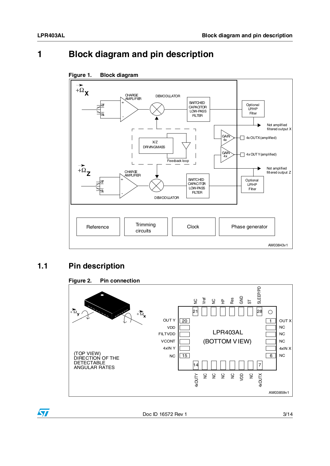
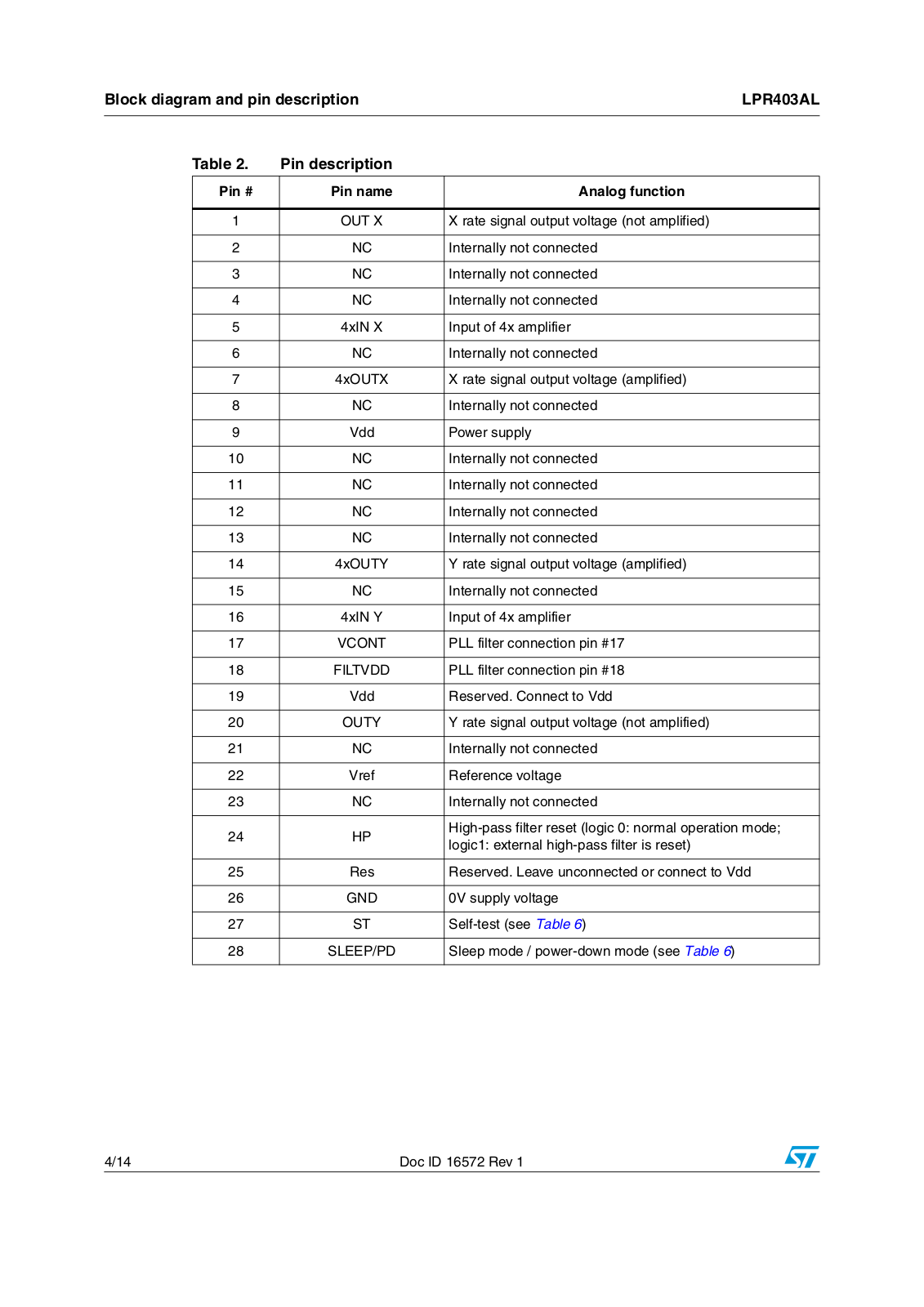
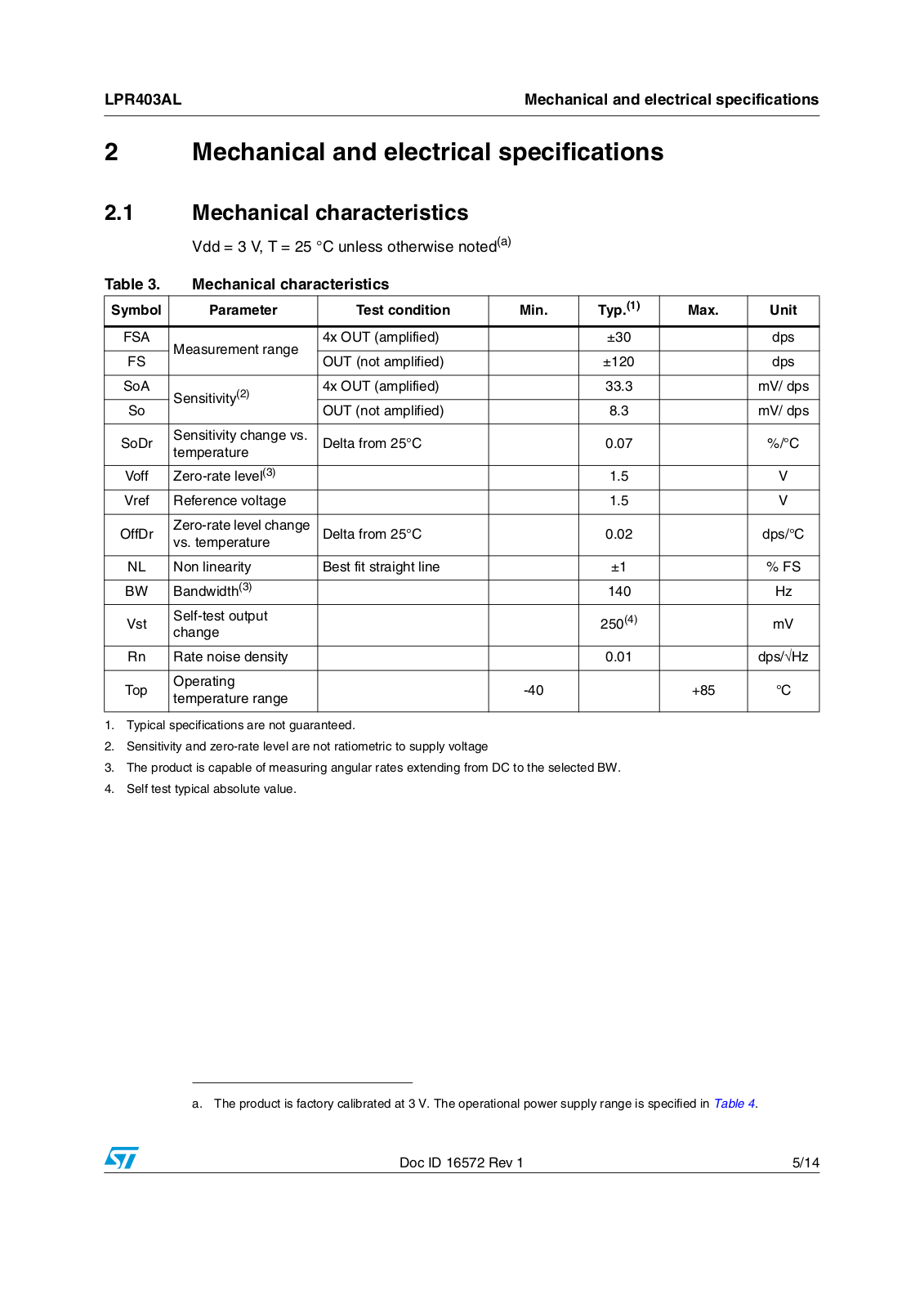
LPR403AL
LPS22HB
LPS25H
LPS25HB
LPS331AP
2
LPY4150AL
LPY450AL
LRI1K
LRI2K
LRIS2K
LRIS64K
LS204
LS404
LSM303D
LSM303DLHC
LSM303DLM
LSM320DL
LSM320HAY30
LSM330
LSM330D
LSM330DL
LSM330DLC
LSM333D
LY3100ALH
LY3200ALH
LY330ALH
M
M1
M22100
M24128-125
M24128-B
M24128-BF
M24128-BR
2
M24128-BW
2
M24128-DF
M24164
M24256-125
M24256-A
M24256-B
M24256-BF
M24256-BR
2
M24256-BW
2
M24256-DF
M24256-DR
M24512
M24512-125
M24512-DF
M24512-DR
M24512-R
M24512-W
M24C01
3
Loading...
Loading...
Nothing found
LPR403AL
User Manual
14 pgs
263.22 Kb
0
Table of contents
Loading...
ST LPR403AL User Manual
...
ST User Manual
Download
Specifications and Main Features
Frequently Asked Questions
User Manual
Download
Loading...
+
9
hidden pages
Unhide
You need points to download manuals.
1 point = 1 manual.
You can buy points or you can get point for every manual you upload.
Buy points
Upload your manuals
 Loading...