

LNB supply and control voltage regulator
Features
■ Simplest integrated solution for LNB remote
supply and control
■ 500 mA guaranteed output current
■ Dual input supply for reducing power
dissipation (DFN package)
■ 3-state function to enable/disable and select
the output voltage level through a single pin
■ Fast oscillator startup for DiSEq™ encoding
(LNBP9L/11L versions)
■ External 22 kHz modulation input pin
(LNBP8L/10L versions)
■ Cable length compensation, LLC pin
(LNBP10L, LNBP11L versions)
■ Short-circuit and over-temperature protection
■ LNB overload and short-circuit dynamic
protection (LNBP10L, LNBP11L versions)
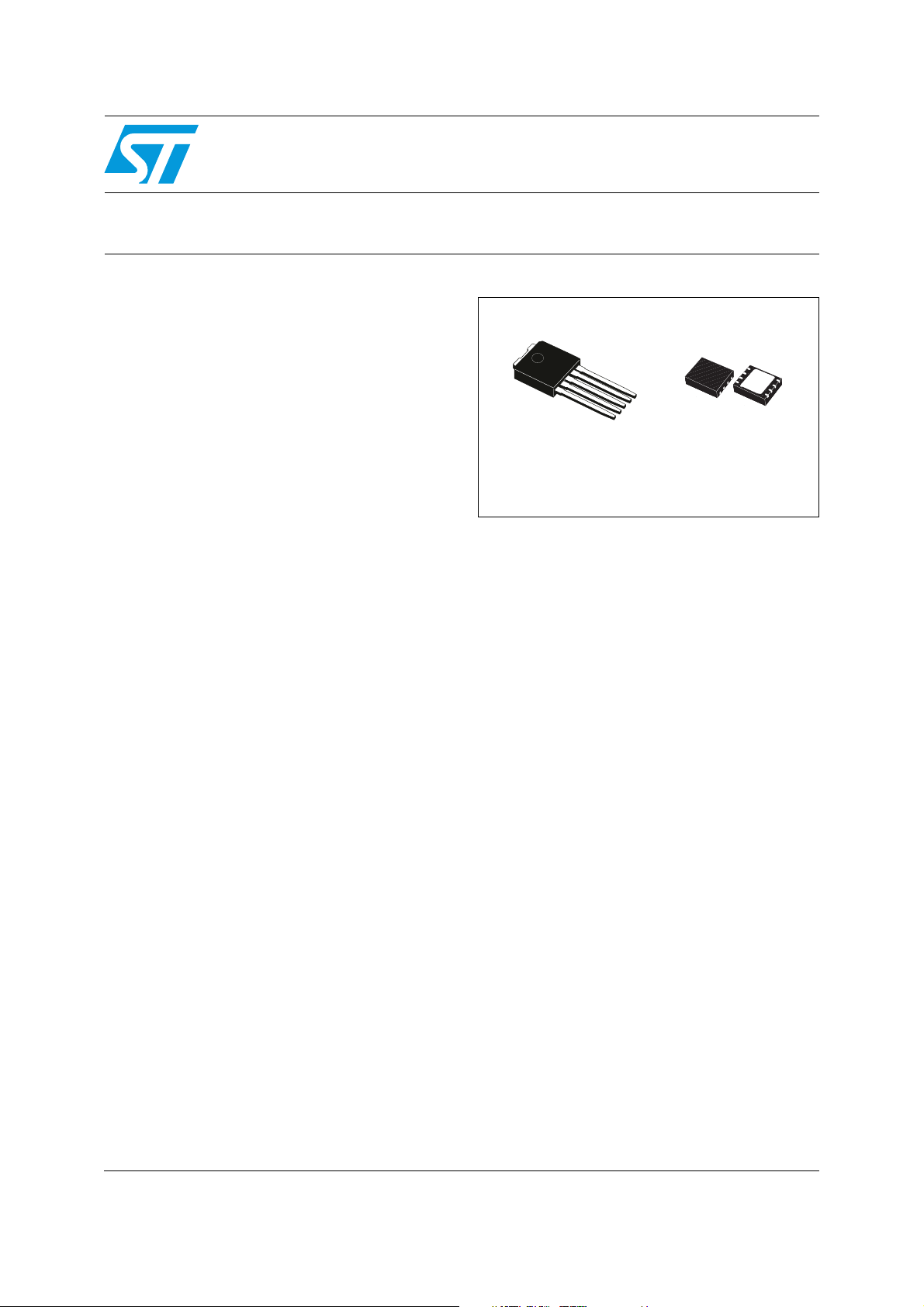
■ Available in DFN8 (5 x 6 mm) and IPPAK
packages
Description
Intended for analog and digital satellite receivers,
the LNBP is a monolithic linear voltage regulator,
assembled in the DFN8 (5 x 6) and IPPAK
packages, specifically designed to provide the
powering voltages and the interfacing signals to
the LNB down-converter. The regulator output
can be logic controlled for 13 V or 18 V (typ.) by
means of the EN/VSEL 3-state pin for remotely
controlling the LNB. When the IC is powered and
put in standby (EN/VSEL pin at high impedance),
the regulator output is disabled. In order to reduce
power dissipation, the LNBP10L/11L versions (on
DFN package) feature 2 supply inputs: V
V
. These pins must be powered, respectively,
CC2
at 15 V (min.) and 22 V (min.), and an internal
switch will automatically select the appropriate
supply voltage according to the selected output
voltage. The LNBP8L/9L versions (in the IPPAK
package) have only one supply input pin, which
CC1
and
LNBP8L, LNBP9L
LNBP10L, LNBP11L
IPPAK
must be supplied at 22 V (min.). Additionally, the
LNBP10L/11L versions have the LLC pin to
increment the selected output voltage value by 1
V (typ.) to compensate for the excess voltage
drop along the coaxial cable (LLC pin HIGH). An
analog 22 kHz modulation input pin (EXTM) is
available in the LNBP8L and LNBP10L versions.
An appropriate DC blocking capacitor must be
used to couple the modulating signal source to
the EXTM pin. The LNBP10L/11L versions are
also equipped with over-current dynamic
protection: as soon as an overload is detected the
output is shut down for the time T
determined by the capacitor connected between
the CEXT pin and GND. After the time has
elapsed, the output is resumed for a time T
(1/12)*T
(typ.). If the overload is still present,
OFF
the protection circuit will cycle again through T
and T
T
ON+TOFF
until the overload is removed. A typical
ON
value is 1100 ms when a 4.7 µF
external capacitor is used on the C
dynamic operation can greatly reduce the power
dissipation in short-circuit condition, while
ensuring excellent power-on startup even with
highly capacitive loads on the LNB outputs. The
device is packaged in the IPPAK for through-hole
mounting and in the DFN8 (5 x 6) for surface
mounting. Both package solutions are offered in
two versions: with ten pins (LNBP9L/11L) to use
with the integrated 22 kHz tone generator, or with
the EXTM pin (LNBP8L/10L) to use external 22
kHz sources. All versions have built-in thermal
protection to prevent overheating damage.
DFN8 (5 x 6 mm)
which is
OFF,
ON
. This
EXT
=
OFF
August 2010 Doc ID 15153 Rev 2 1/21
www.st.com
21

Contents LNBP8L, LNBP9L, LNBP10L, LNBP11L
Contents
1 Diagram . . . . . . . . . . . . . . . . . . . . . . . . . . . . . . . . . . . . . . . . . . . . . . . . . . . 3
2 Pin configuration . . . . . . . . . . . . . . . . . . . . . . . . . . . . . . . . . . . . . . . . . . . . 4
3 Maximum ratings . . . . . . . . . . . . . . . . . . . . . . . . . . . . . . . . . . . . . . . . . . . . 5
4 Electrical characteristics . . . . . . . . . . . . . . . . . . . . . . . . . . . . . . . . . . . . . 6
5 Typical application circuits . . . . . . . . . . . . . . . . . . . . . . . . . . . . . . . . . . . 8
6 Detailed description and application hints . . . . . . . . . . . . . . . . . . . . . . . 9
6.1 Input voltage protection . . . . . . . . . . . . . . . . . . . . . . . . . . . . . . . . . . . . . . 10
6.2 Single supply for the DFN package . . . . . . . . . . . . . . . . . . . . . . . . . . . . . 10
6.3 IPPAK mounting and thermal considerations . . . . . . . . . . . . . . . . . . . . . . 11
7 Typical performance characteristics . . . . . . . . . . . . . . . . . . . . . . . . . . . 13
8 Package mechanical data . . . . . . . . . . . . . . . . . . . . . . . . . . . . . . . . . . . . 16
9 Ordering information . . . . . . . . . . . . . . . . . . . . . . . . . . . . . . . . . . . . . . . 19
10 Revision history . . . . . . . . . . . . . . . . . . . . . . . . . . . . . . . . . . . . . . . . . . . 20
2/21 Doc ID 15153 Rev 2
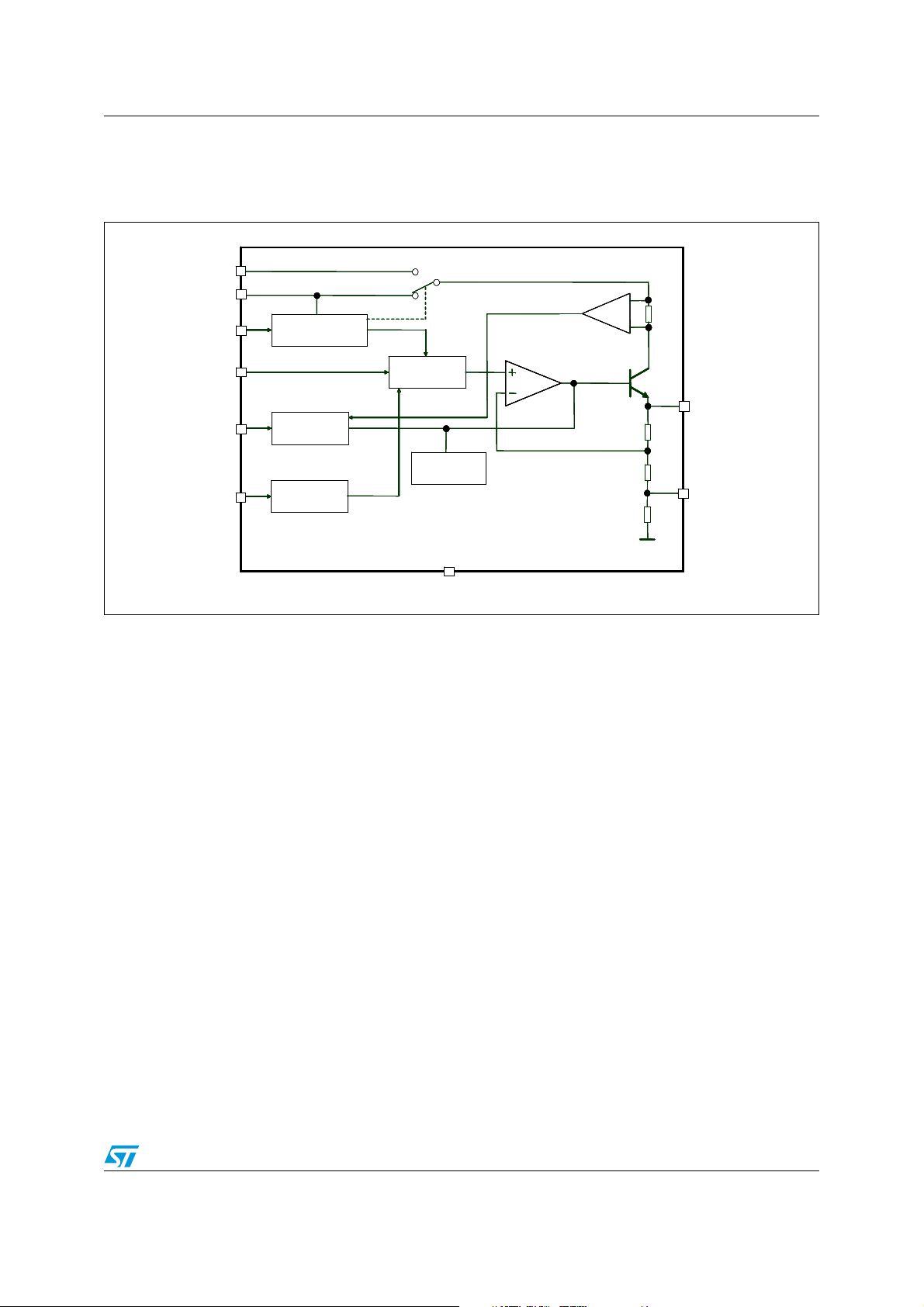
LNBP8L, LNBP9L, LNBP10L, LNBP11L Diagram
1 Diagram
Figure 1. Block diagram
VCC1
VCC1
VCC1
VCC1
VCC2
VCC2
VCC2
VCC2
R
R
R
R
SENSE
SENSE
SENSE
EN/VSEL
EN/VSEL
EN/VSEL
EN/VSEL
LLC
LLC
LLC
LLC
CEXT
CEXT
CEXT
CEXT
TEN
TEN
TEN
TEN
TRISTATE ENABLE &
TRISTATE ENABLE &
TRISTATE ENABLE &
TRISTATE ENABLE &
VOUT SELECTION
VOUT SELECTION
VOUT SELECTION
VOUT SELECTION
DYNAMIC
DYNAMIC
DYNAMIC
DYNAMIC
CURRENT LIMIT
CURRENT LIMIT
CURRENT LIMIT
CURRENT LIMIT
22KHz
22kHz
22KHz
22kHz
OSCILLATOR
OSCILLATOR
OSCILLATOR
OSCILLATOR
VOLTAGE
VOLTAGE
VOLTAGE
VOLTAGE
VOLTAGE
VOLTAGE
REFERENCE
REFERENCE
REFERENCE
REFERENCE
REFERENCE
REFERENCE
THERMAL
THERMAL
THERMAL
THERMAL
PROTECTION
PROTECTION
PROTECTION
PROTECTION
SENSE
OUTPUT
OUTPUT
OUTPUT
OUTPUT
EXTM
EXTM
EXTM
EXTM
LNBP8L/9L/10L/11L
LNBP8L/9L/10L/11L
LNBP8L/9L/10L/11L
LNBP8L/9L/10L/11L
GND
GND
GND
GND
Doc ID 15153 Rev 2 3/21
Pin configuration LNBP8L, LNBP9L, LNBP10L, LNBP11L
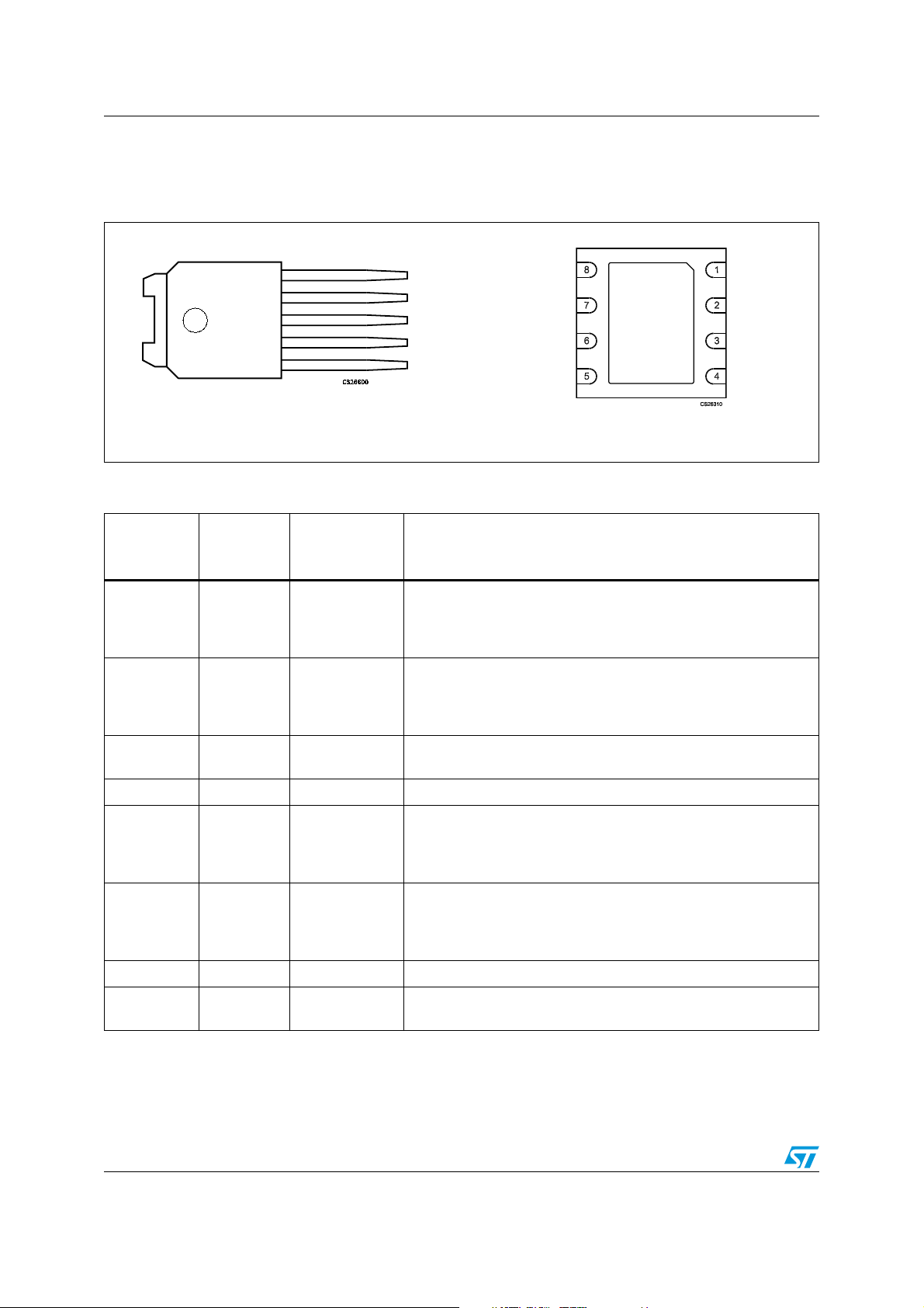
2 Pin configuration
Figure 2. Pin connections (top view for IPPAK, bottom view for DFN8)
IPPAK
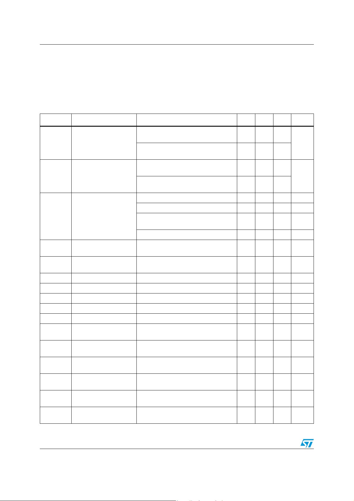
Table 1. Pin description
Pin n° (DFN)
LNBP10/11L
1-
21
32OUTPUT
4, ePAD 3, ePAD GROUND GROUND
64EN/VSEL
55EXTM/TEN
Pin n°
(IPPAK)
LNBP8/9L
Name Pin function
VCC1
(not available for
IPPAK)
VCC2
pin for
(V
CC
IPPAK)
Supply input 1: 15 V to 25 V supply. For DFN package it is
automatically selected when V
V
supplied at 22 V min.
Supply input 2: 22 V to 25 V supply. For DFN package it is
automatically selected when V
V
supplied at 22 V min.
Output: regulator output. It is 13 V typ when EN/VSEL LOW and
18 V typ when EN/VSEL HIGH.
Enable and output voltage selection 3-state pin: logic control
input 3-state pin for the remote controlling of the LNB; if LOW
V
IC is set in shut down mode (V
Tone enable (LNBP9-11): logic control input to enable internal
tone generator.
External modulation (LNBP8-10): Needs DC decoupling to the
AC source. If not used can be left floating.
and V
CC1
and V
CC1
= 13 V, when HIGH V
OUT
are internally connected together to pin 1 to be
CC2
are internally connected together to the pin 1 to be
CC2
DFN8 (5 x 6 mm)
= 13 V. For IPPAK package
OUT
= 18 V. For IPPAK package
OUT
= 18 V, if left at high impedance the
OUT
OUT
= 0 V)
8 NA LLC LLC: logic control input to add 1 V typ.
C
: timing capacitor used by the dynamic overload protection.
7NAC
EXT
EXT
Typical application is 4.7 µF for a 1100 ms cycle
4/21 Doc ID 15153 Rev 2
LNBP8L, LNBP9L, LNBP10L, LNBP11L Maximum ratings
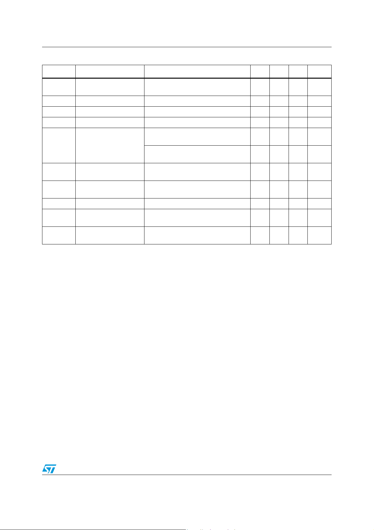
3 Maximum ratings
Table 2. Absolute maximum ratings
Symbol Parameter Value Unit
VCC1, VCC2 Input voltages -0.3 to 28 V
VCC1-OUTPUT VCC1 voltage with respect to OUTPUT voltage
VCC2-OUTPUT VCC2 voltage with respect to OUTPUT voltage
EN/VSEL, TEN,
LLC
EXTM External modulation input voltage -0.3 to 1 V
OUTPUT Output voltage -0.3 to 25 V
T
STG
ESD
DFN package
Logic input voltage -0.3 to 7 V
Storage temperature range -50 to 150 °C
ESD rating with human body model (HBM) for all pins except 1, 2, 6 2 kV
ESD rating with human body model (HBM) for pins 1, 2, 6 1.5
(1)
(1)
-0.3 to 25 V
-0.3 to 25 V
ESD
IPPAK package
1. Exposure beyond the VCC1 and VCC2 with respect to OUTPUT absolute-maximum-rated voltages during OUTPUT pin
overload or short-circuit to GROUND may cause permanent damage to the device.
ESD rating with human body model (HBM) for all pins except 1, 4 2 kV
ESD rating with human body model (HBM) for pins 1, 4 1.5
Note: Absolute maximum ratings are those values beyond which damage to the device may occur.
These are stress ratings only and functional operation of the device at these conditions is
not implied. Exposure to absolute-maximum-rated conditions for extended periods may
affect device reliability. All voltage values are with respect to network ground terminal unless
otherwise stated.
Table 3. Operating ratings
Symbol Parameter Value Unit
T
J
VCC1 Input voltage 15 to 25 V
VCC2 Input voltage 22 to 25 V
Operating junction temperature range 0 to 125 °C
Table 4. Thermal data
Symbol Parameter IPPAK DFN8 Unit
R
R
Thermal resistance junction-ambient
thJA
Thermal resistance junction-case 8 °C/W
thJC
Doc ID 15153 Rev 2 5/21
(mounted on PCB 2s2p)
35
°C/W
Electrical characteristics LNBP8L, LNBP9L, LNBP10L, LNBP11L
4 Electrical characteristics
Refer to the typical application circuits in Figure 3 and Figure 4, V
V
= 23 V
CC2
T
= 0 °C to 85 °C, unless otherwise stated. Typical values are referred to TJ = 25 °C.
J
Table 5. Electrical characteristics
(1)
, EN/VSEL = LOW, TEN = LLC = LOW, EXTM = FLOATING, I
CC1
= 16 V,
OUT
= 50 mA,
Symbol Parameter Test conditions Min. Typ. Max. Unit
I
= 500 mA, TEN=HIGH,
V
V
V
ΔV
ΔV
I
F
A
D
G
V
Z
CC1
CC2
OUT
OUT
OUT
MAX
TONE
TONE
TONE
, t
t
r
EXTM
EXTM
EXTM
OUT
VCC supply input 1
(1)
EN/VSEL=LOW, LLC=LOW
I
= 500 mA, TEN=HIGH,
OUT
EN/VSEL=LOW, LLC= HIGH
I
= 500 mA, TONE=HIGH,
OUT
VCC supply input 2
(1)
EN/VSEL=HIGH, LLC=LOW
= 500 mA, TONE=HIGH,
I
OUT
EN/VSEL=HIGH, LLC= HIGH
I
= 500 mA, EN/VSEL=LOW 12.5 13.25 14 V
OUT
= 500 mA, EN/VSEL=HIGH 17 18 19 V
I
OUT
Output voltage
Line regulation
Load regulation
(1)
I
= 500 mA, EN/VSEL=LOW,
OUT
LLC=HIGH
I
OUT
V
CC1
(2)
= 500 mA, EN/VSEL=LLC=HIGH
from 15 V to 18 V, EN/VSEL=LOW
or HIGH
V
CC1
= V
CC2
= 22 V, I
from 50 mA to
OUT
500 mA, EN/VSEL=LOW or HIGH
Output current limiting 550 700 850 mA
Tone frequency TEN=High 20 22 24 kHz
Tone amplitude TEN=High 0.4 0.65 0.9 V
Tone duty cycle TEN=High 40 50 60 %
/Δ V
(3)
, freq. from 10 kHz to 40
EXTM
Tone Rise and Fall Time TEN=High
f
External modulation Gain
External modulation input
voltage
External modulation
impedance
Δ V
OUT
kHz
AC Coupling 400 mV
Freq. from 10 kHz to 40 kHz 400 Ω
15 25
16 25
22 25
23 25
14.25 V
(2)
19 V
540mV
50 150 mV
51015µs
4.5 5.5 6.5
V
V
PP
PP
V
ILT
V
IHT
I
IHT
Control input logic LOW
threshold for 3-state pin
Control input logic HIGH
threshold for 3-state pin
3-state control pin input
current HIGH
EN/VSEL 0.8 1 1.2 V
EN/VSEL 1.8 2 2.2 V
V
= 5 V, EN/VSEL -400 µA
IHT
6/21 Doc ID 15153 Rev 2
LNBP8L, LNBP9L, LNBP10L, LNBP11L Electrical characteristics
Table 5. Electrical characteristics (continued)
Symbol Parameter Test conditions Min. Typ. Max. Unit
I
ILT
V
V
I
IH
I
CC
T
OFF
T
ON
I
OBK
T
SHDN
ΔT
SHDN
1. For IPPAK package V
25 V
2. Only DFN package
3. Guaranteed by design
3-state control pin input
current LOW
Control input logic LOW TEN, LLC 0.8 V
IL
Control input logic HIGH TEN, LLC 2.5 V
IH
Control pins input current V
Supply current
Dynamic overload
protection OFF time
Dynamic overload
protection ON time
Output backward current Output forced to 21 V 6 mA
Thermal shutdown
threshold
Thermal shutdown
hysteresis
CC1
and V
= 0 V, EN/VSEL +180 µA
V
ILT
= 5 V, TEN, LLC 20 µA
IH
Output disabled EN/VSEL=High
impedance (floating)
Output enabled EN/VSEL=HIGH,
TEN=HIGH, I
Output shorted, C
Output shorted, C
OUT
= 500 mA
= 4.7 µF
EXT
= 4.7 µF
EXT
(2)
(2)
1.7 2.4 mA
3.7 6.3 mA
1000 ms
T
OFF
/12
165 °C
25 °C
are internally connected to the pin 1 (VCC) to be supplied in the range from 22 V up to
CC2
ms
Doc ID 15153 Rev 2 7/21

Typical application circuits LNBP8L, LNBP9L, LNBP10L, LNBP11L
5 Typical application circuits
Figure 3. Single input supply voltage solution for IPPAK package versions
D1
D1
D1
C1
C1
C1
C1
10µF
10µF
10µF
10µF
C4
C4
C4
C4
10µF
10µF
10µF
10µF
D1
1N4001
1N4001
1N4001
1N4001
MCU I/Os
MCU I/Os
MCU I/Os
MCU I/Os
D3 1N4001
D3 1N4001
D3 1N4001
D3 1N4001
MCU I/Os
MCU I/Os
MCU I/Os
MCU I/Os
C2
C2
C2
C2
220nF
220nF
220nF
220nF
D1 1N4001
D1 1N4001
D1 1N4001
D1 1N4001
C2
C2
C2
C2
220nF
220nF
220nF
220nF
C5
C5
C5
C5
220nF
220nF
220nF
220nF
VCC
VCC
VCC
VCC
LNBP8/9L
LNBP8/9L
LNBP8/9L
LNBP8/9L
EN/VSEL (Tristate )
EN/VSEL (Tristate)
EN/VSEL (Tristate )
EN/VSEL (Tristate)
EXTM or TEN
EXTM or TEN
EXTM or TEN
EXTM or TEN
GND
GND
GND
GND
VCC1
VCC1
VCC1
VCC1
VCC2
VCC2
VCC2
VCC2
LNBP10/11L
LNBP10/11L
LNBP10/11L
LNBP10/11L
LLC
LLC
LLC
LLC
EN/VSEL (Tristate)
EN/VSEL (Tristate
EN/VSEL (Tristate)
EN/VSEL (Tristate
EXTM or TEN
EXTM or TEN
EXTM or TEN
EXTM or TEN
GND
GND
GND
GND
OUTPUT
OUTPUT
OUTPUT
OUTPUT
OUTPUT
OUTPUT
OUTPUT
OUTPUT
CEXT
CEXT
CEXT
CEXT
D2
D2
D2
D2
1N5818
1N5818
1N5818
1N5818
D2
D2
D2
D2
1N5818
1N5818
1N5818
1N5818
23V
23V
23V
23V
C1
C1
C1
C1
10µF
10µF
10µF
10µF
Figure 4. Dual input supply voltage solution for DFN8 (5 x 6 mm) package versions
16V
16V
16V
16V
23V
23V
23V
23V
LNB OUTPUT
LNB OUTPUT
LNB OUTPUT
LNB OUTPUT
C3
C3
C3
C3
100nF
100nF
100nF
100nF
LNB OUTPUT
LNB OUTPUT
LNB OUTPUT
LNB OUTPUT
C3
C3
C3
C3
100nF
100nF
100nF
100nF
C6
C6
C6
C6
4.7µF
4.7µF
4.7µF
4.7µF
Figure 5. Single input supply voltage solution for DFN8 (5 x 6 mm) package versions
D1
D1
D1
23V
23V
23V
23V
C1
C1
C1
C1
10µF
10µF
10µF
10µF
D1
1N4001
1N4001
1N4001
1N4001
R1
R1
R1
R1
15 Ohm >3W
15 Ohm >3W
15 Ohm >3W
15 Ohm >3W
MCU I/Os
MCU I/Os
MCU I/Os
MCU I/Os
C2
C2
C2
C2
220nF
220nF
220nF
220nF
C4
C4
C4
C4
220nF
220nF
220nF
220nF
VCC1
VCC1
VCC1
VCC1
VCC2
VCC2
VCC2
VCC2
LNBP10/11L
LNBP10/11L
LNBP10/11L
LNBP10/11L
LLC
LLC
LLC
LLC
EN/VSEL (Tristate )
EN/VSEL (Tristate )
EN/VSEL (Tristate )
EN/VSEL (Tristate )
EXTM or TEN
EXTM or TEN
EXTM or TEN
EXTM or TEN
GND
GND
GND
GND
OUTPUT
OUTPUT
OUTPUT
OUTPUT
CEXT
CEXT
CEXT
CEXT
D2
D2
D2
D2
1N5818
1N5818
1N5818
1N5818
LNB OUTPUT
LNB OUTPUT
LNB OUTPUT
LNB OUTPUT
C3
C3
C3
C3
100nF
100nF
100nF
100nF
C5
C5
C5
C5
4.7µF
4.7µF
4.7µF
4.7µF
Note: In a single supply configuration with the DFN package, an R1 resistor in the 12-15 Ω range
is recommended to reduce device power dissipation during the 13 V output condition. The
resistor can be omitted, but the power dissipation will increase.
8/21 Doc ID 15153 Rev 2

LNBP8L, LNBP9L, LNBP10L, LNBP11L Detailed description and application hints
6 Detailed description and application hints
The LNBPxx is made up of several functional blocks (see Figure 1 on page 3), as described
below:
1. The oscillator is activated by setting the ENT pin (enable tone) = H, and is factorytrimmed at 22 kHz ± 2 kHz, eliminating the need to use external trimming. The rising
and falling edges are maintained in the 5 to 15 µs range (10 µs typ.), to avoid RF
pollution of the receiver. The duty cycle is 50% typ. It modulates the DC output with a ±
0.325 V typ. amplitude and 0 V average. The presence of this signal usually gives the
LNB information about the band to be received.
2. The 3-state enable & V
IC to shutdown mode, depending on the voltage applied on the EN/VSEL pin.
When EN/VSEL is set high (EN/VSEL > 2.2 V), an 18 V output voltage is selected;
when the EN/VSEL is set low (EN/VSEL < 0.8 V), a 13 V output voltage is selected.
If the EN/VSEL pin is left floating (high impedance) or if the pin is set in a range from
1.2 V to 1.8 V (1.5 V typ.), the IC goes into shutdown mode and the output voltage will
be set to 0 V.
This feature changes the LNB polarization type. The LNB switches to horizontal or
vertical polarization depending on the supply voltage it gets from the receiver.
3. For the DFN package, in order to keep the power dissipation of the device as low as
possible, the input selector automatically selects V
when 13 V output is selected (i.e. EN/VSEL is low). If the 18 V output is selected (i.e.
EN/VSEL is high), the V
I
= 350 mA is:
OUT
P
= (23 - 18) x 0.35 = 1.75 W
D
with V
P
= (16 - 13) x 0.35 = 1.05 W
D
with V
For IPPAK package, V
= 23 V (voltage on the V
CC2
= 16 V (voltage on the V
CC1
CC1
single input voltage line (22 V min.) to the V
dissipation is 13 V output. For example: at I
V
pin):
CC
P
= (23 - 13) x 0.35 = 3.5 W
D
4. The line length compensation function is useful when the antenna is connected to the
receiver by a long coaxial cable that adds a considerable DC voltage drop. When the
LCC pin is H, the output voltage selected is increased by about 1 V. This function is
available for the DFN package only.
5. The reference drives all the internal blocks that require a high-precision thermally
compensated voltage source.
6. The LNBPxx has two different protection features, and both turn off the outputs. The
first one protects against overheating (i.e. for T
overload conditions (i.e. for output current > 550 mA) or short-circuit:
a) In the thermal protection case the output is disabled until the chip temperature has
fallen below 140 °C typ. and the LNBPxx output is restored.
b) The overload protection case occurs when output current request is ≥ 500 mA. For
the DFN package only, the IC features dynamic overload and short-circuit
protection. When an overload occurs the device limits the output current for the
selection block, selects the two output voltages or sets the
OUT
; that is, the lowest input voltage,
CC1
input pin is selected. For example, power dissipation at
CC2
and V
pin) and V
CC2
pin) and V
CC1
are internally connected and must be supplied from a
CC2
pin. In this case the worst case power
CC
OUT
= 18 V, and
OUT
= 13 V
OUT
= 350 mA and V
≥ 150 °C), and the second against
J
= 23 V (voltage on the
CC
Doc ID 15153 Rev 2 9/21

Detailed description and application hints LNBP8L, LNBP9L, LNBP10L, LNBP11L
time TON depending on the C
has elapsed, the output goes low for a time of T
power dissipated by the device low in overload conditions, and avoids the need for
an oversized heat sink in this condition. For the IPPAK package, when the
overload or the short-circuit occurs, the device clamps the output current in a
range between 550 mA and 850 mA.
7. EXTM modulates the V
The following equation is used to calculate the peak-to-peak voltage of V
Equation 1
V
(AC) = V
OUT
where V
V
EXTM
Figure 6. EXTM application circuit
23V
C1
10µF
. G
OUT
EXTM
D1
1N4001
(AC) and V
C2
220nF
(AC) x G
EXTM
EXTM
is the external modulation gain.
value (see Figure 24 and Figure 25). When TON
EXT
by means of a capacitor connected in series (see Figure 6).
OUT
EXTM
(AC) are, respectively, the peak-to-peak voltage of V
VCC
OUTPUT
LNBP8/9L
= 12 x TON. This keeps the
OFF
OUT
LNB OUTPUT
D2
1N5818
C3
100nF
:
OUT
and
EN/VSEL (Tristate)
Vextm
C4
1µF
EXTM
GND
6.1 Input voltage protection
In some cases two or more receivers share the same coaxial cable, rendering their outputs
hard-paralleled, so the same voltage is present at the outputs of the receivers. If a receiver
is not disconnected at the mains, a current will flow from the OUTPUT to the V
pins, depending the EN/VSEL pin setting. To avoid this, two diodes (only one for the IPPAK
package) in series are recommended at input pins V
diodes do not cause a change at V
, but only a voltage drop, which can be minimized by
OUT
using Schottky diodes. Diodes used in Figure 4 and Figure 5 must withstand a continuous
current of almost 1 A and a breakdown voltage of 30 V (suggested type is 1N4001 or
BYV10-30). Be aware that the minimum voltage needed at the V
considering the voltage drop across the input diodes).
6.2 Single supply for the DFN package
If only one power supply source is available, the V
same power source without affecting the performance of other circuits, at the cost of higher
power losses in the device and higher heat sink surface. Also, in order to reduce the power
dissipation in the device, an appropriate-value resistor can be inserted in series with the
CC1
and V
CC1
and V
or V
CC1
(see Figure 3). These
CC2
pins must be respected,
CC
pins can be powered by the
CC2
CC2
10/21 Doc ID 15153 Rev 2
LNBP8L, LNBP9L, LNBP10L, LNBP11L Detailed description and application hints
V
line (see Figure 5). This resistor must be dimensioned considering that the minimum
CC1
voltage on the V
For example, with I
pin must be >= 16 V (15 V if LLC is not used).
CC1
= 500 mA:
OUT
Equation 2
--
--
16)(23
16)(23
V
V
f
≤
≤
R
R
f
10x500
10x500
≅
≅
12 Ω
-3
-3
12 Ω
Where V
is the forward voltage of the input diode D1 (see Figure 5).
f
Power dissipated in this resistor is:
Equation 3
2
2
-
-
32
32
===
RP
RP
D
D
It is recommended to bypass the V
I
I
OUT
OUT
CC1
and V
()
()
pins using 220 nF electrolytic capacitors.
CC2
===
3 W10*500*12*
3 W10*500*12*
6.3 IPPAK mounting and thermal considerations
First, it should be noted that the tab is directly connected to the GND pin, so care must be
taken when the device is connected to a heat-sink. If the heat sink is at a different voltage
than the ground, an electrical insulator must be added between the tab and the heat sink at
the cost of an increase in the thermal resistance. For better thermal performance, an
isolated heat sink or connection to ground is recommended.
Several clips can be used depending on the heat sink type:
● Saddle clips (Figure 7) for slim heat sinks
● U-clips (Figure 8) for thick heat sinks
● Dedicated clips for special shaped heat sinks
Figure 7. IPPAK mounted with a saddle clip
Doc ID 15153 Rev 2 11/21

Detailed description and application hints LNBP8L, LNBP9L, LNBP10L, LNBP11L
Figure 8. IPPAK mounted with a U-clip
Note that the thickness of the IPPAK package (2.3 +/- 0.1 mm) is similar to that of the SOT32 and SOT-82 (2.55 +/- 0.15 mm). The same clips can also be used for these packages.
The junction-to-ambient thermal resistance for the IPPAK can be calculated as follows:
Equation 4
R
= R
TH-JA
where: R
data
), R
TH-JC
TH-CH
+ R
TH-JC
TH-CH
is the junction-to-case thermal resistance of the IPPAK (see Ta bl e 4 : Th er ma l
is the case-to-heat sink thermal resistance and the R
air thermal resistance.
+ R
TH-HA
is the heat sink-to-
TH-HA
12/21 Doc ID 15153 Rev 2

LNBP8L, LNBP9L, LNBP10L, LNBP11L Typical performance characteristics
7 Typical performance characteristics
Refer to the typical application circuit, TJ from 0 to 85 °C. Typical values are referred to
T
= 25 °C.
J
Figure 9. Output voltage vs. temperature Figure 10. Output voltage vs. temperature
14
14
V
= 15 V
V
= 15 V
13.8
13.8
CC1
CC1
= 23 V
= 23 V
V
V
CC2
CC2
13.6
13.6
= 50 mA
= 50 mA
I
I
OUT
OUT
13.4
13.4
= 13 V
= 13 V
V
V
OUT
OUT
13.2
13.2
[V]
[V]
13
13
OUT
OUT
12.8
12.8
V
V
12.6
12.6
12.4
12.4
EN/VSEL=L
EN/VSEL=L
12.2
12.2
TEN=L, LLC=L
TEN=L, LLC=L
12
12
-10 0 102030 405060708090
-10 0 102030 405060708090
T [°C]
T [°C]
Figure 11. Output voltage vs. temperature Figure 12. Output voltage vs. temperature
H = Logic High = 5 V
H = Logic High = 5 V
L = Logic Low = 0 V
L = Logic Low = 0 V
14
14
V
= 15 V
V
= 15 V
13.8
13.8
CC1
CC1
= 23 V
= 23 V
V
V
CC2
CC2
13.6
13.6
I
I
= 500 mA
= 500 mA
OUT
OUT
13.4
13.4
V
V
= 13 V
= 13 V
OUT
OUT
13.2
13.2
[V]
[V]
13
13
OUT
OUT
12.8
12.8
V
V
12.6
12.6
12.4
12.4
EN/VSEL=L
EN/VSEL=L
12.2
12.2
TEN=L, LLC=L
TEN=L, LLC=L
12
12
-10 0 10 20 30 40 50 60 70 80 90
-10 0 10 20 30 40 50 60 70 80 90
T [°C]
T [°C]
H = Logic High = 5 V
H = Logic High = 5 V
L = Logic Low = 0 V
L = Logic Low = 0 V
19
19
V
= 15 V
V
= 15 V
CC1
CC1
18.8
18.8
18.6
18.6
18.4
18.4
18.2
18.2
[V]
[V]
OUT
OUT
17.8
17.8
V
V
17.6
17.6
17.4
17.4
17.2
17.2
Figure 13. Line regulation vs. temperature Figure 14. Load regulation vs. temperature
Line Reg. [mV]
Line Reg. [mV]
= 23 V
= 23 V
V
V
CC2
CC2
= 50 mA
= 50 mA
I
I
OUT
OUT
= 18 V
= 18 V
V
V
OUT
OUT
18
18
H = Logic High = 5 V
EN/VSEL=H
EN/VSEL=H
TEN=L, LLC=L
TEN=L, LLC=L
17
17
-10 0 10 20 30 40 50 60 70 80 90
-10 0 10 20 30 40 50 60 70 80 90
T [°C]
T [°C]
50
50
V
= 16 V to 25 V
V
= 16 V to 25 V
CC1
CC1
40
40
V
V
= 23 V
= 23 V
CC2
CC2
= 50 mA
= 50 mA
I
I
30
30
OUT
OUT
V
V
= 13 V
= 13 V
OUT
OUT
20
20
10
10
0
0
-10
-10
-20
-20
-30
-30
EN/VSEL=L
EN/VSEL=L
-40
-40
TEN=L, LLC=L
TEN=L, LLC=L
-50
-50
-10 0 10 20 30 40 50 60 70 80 90
-10 0 10 20 30 40 50 60 70 80 90
T [°C]
T [°C]
H = Logic High = 5 V
L = Logic Low = 0 V
L = Logic Low = 0 V
H = Logic High = 5 V
H = Logic High = 5 V
L = Logic Low = 0 V
L = Logic Low = 0 V
19
19
V
= 15 V
V
= 15 V
CC1
CC1
18.8
18.8
18.6
18.6
18.4
18.4
18.2
18.2
[V]
[V]
OUT
OUT
17.8
17.8
V
V
17.6
17.6
17.4
17.4
17.2
17.2
Load [mV]
Load [mV]
-100
-100
-150
-150
-200
-200
-250
-250
= 23 V
= 23 V
V
V
CC2
CC2
= 500 mA
= 500 mA
I
I
OUT
OUT
= 18 V
= 18 V
V
V
OUT
OUT
18
18
EN/VSEL=H
EN/VSEL=H
TEN=L, LLC=L
TEN=L, LLC=L
17
17
-10 0 10 20 30 40 5 0 60 70 80 90
-10 0 10 20 30 40 5 0 60 70 80 90
T [°C]
T [°C]
250
250
V
= 15 V
V
= 15 V
CC1
CC1
200
200
150
150
100
100
= 23 V
= 23 V
V
V
CC2
CC2
= from 50 mA to 500 mA
= from 50 mA to 500 mA
I
I
OUT
OUT
V
V
= 13 V
= 13 V
OUT
OUT
50
50
0
0
-50
-50
EN/VSEL=L
EN/VSEL=L
TEN=L, LLC=L
TEN=L, LLC=L
-10 0 10 20 30 40 50 60 70 80 90
-10 0 10 20 30 40 50 60 70 80 90
T [°C]
T [°C]
H = Logic High = 5 V
H = Logic High = 5 V
L = Logic Low = 0 V
L = Logic Low = 0 V
H = Logic High = 5 V
H = Logic High = 5 V
L = Logic Low = 0 V
L = Logic Low = 0 V
Doc ID 15153 Rev 2 13/21

Typical performance characteristics LNBP8L, LNBP9L, LNBP10L, LNBP11L
Figure 15. Load regulation vs. temperature Figure 16. Output current limiting vs.
250
250
V
= 15 V
V
= 15 V
CC1
CC1
200
200
150
150
100
100
Load [mV]
Load [mV]
-100
-100
-150
-150
= 23 V
= 23 V
V
V
CC2
CC2
= from 50 mA to 500 mA
= from 50 mA to 500 mA
I
I
OUT
OUT
= 18 V
= 18 V
V
V
OUT
OUT
50
50
0
0
-50
-50
EN/VSEL=H
EN/VSEL=H
TEN=L, LLC=L
TEN=L, LLC=L
-10 0 10 20 30 40 50 60 70 80 90
-10 0 10 20 30 40 50 60 70 80 90
T [°C]
T [°C]
H = Logic High = 5 V
H = Logic High = 5 V
L = Logic Low = 0 V
L = Logic Low = 0 V
900
900
850
850
800
800
750
750
700
700
[mA]
[mA]
650
650
LIM
LIM
I
I
600
600
550
550
500
500
450
450
400
400
-10 0 10 20 30 40 50 60 70 80 90
-10 0 10 20 30 40 50 60 70 80 90
temperature
V
= 15 V
V
= 15 V
CC1
CC1
V
V
= 23 V
= 23 V
CC2
CC2
V
V
= 13 V
= 13 V
OUT
OUT
EN/VSEL=L
EN/VSEL=L
TEN=L, LLC=L
TEN=L, LLC=L
T [°C]
T [°C]
H = Logic High = 5 V
H = Logic High = 5 V
L = Logic Low = 0 V
L = Logic Low = 0 V
Figure 17. Output current limiting vs.
900
900
850
850
800
800
750
750
700
700
[mA]
[mA]
650
650
LIM
LIM
I
I
600
600
550
550
500
500
450
450
400
400
-10 0 10 20 30 40 50 60 70 80 90
-10 0 10 20 30 40 50 60 70 80 90
temperature
V
= 15 V
V
= 15 V
CC1
CC1
= 23 V
= 23 V
V
V
CC2
CC2
= 18 V
= 18 V
V
V
OUT
OUT
EN/VSEL=H
EN/VSEL=H
TEN=L, LLC=L
TEN=L, LLC=L
T [°C]
T [°C]
H = Logic High = 5 V
H = Logic High = 5 V
L = Logic Low = 0 V
L = Logic Low = 0 V
Figure 19. Dynamic overload protection OFF
1200
1200
1100
1100
1000
1000
[ms]
[ms]
900
900
OFF
OFF
T
T
800
800
700
700
600
600
time vs. temperature
V
= 15 V
V
= 15 V
CC1
CC1
= 23 V
= 23 V
V
V
CC2
CC2
C
C
= 4.7 µF
= 4.7 µF
ext
ext
V
V
= 13 V
= 13 V
OUT
OUT
EN/VSEL=L
EN/VSEL=L
TEN=L, LLC=L
TEN=L, LLC=L
-10 0 10 20 30 40 50 60 70 80 90
-10 0 10 20 30 40 50 60 70 80 90
T [°C]
T [°C]
H = Logic High = 5 V
H = Logic High = 5 V
L = Logic Low = 0 V
L = Logic Low = 0 V
Figure 18. Dynamic overload protection ON
time vs. temperature
210
210
V
= 16 V
V
= 16 V
CC1
CC1
190
190
170
170
150
150
130
130
[ms]
[ms]
110
110
ON
ON
T
T
= 23 V
= 23 V
V
V
CC2
CC2
C
C
= 4.7 µF
= 4.7 µF
ext
ext
= 13 V
= 13 V
V
V
OUT
OUT
90
90
70
70
50
50
EN/VSEL=L
EN/VSEL=L
30
30
TEN=L, LLC=L
TEN=L, LLC=L
10
10
-10 0 10 20 30 40 50 60 70 80 90
-10 0 10 20 30 40 50 60 70 80 90
T [°C]
T [°C]
H = Logic High = 5 V
H = Logic High = 5 V
L = Logic Low = 0 V
L = Logic Low = 0 V
Figure 20. Tone enable
= 23 V
= 23 V
V
V
CC1
CC1
V
V
= 23 V
= 23 V
CC2
CC2
I
I
= 50 mA
= 50 mA
OUT
OUT
= 13 V
= 13 V
V
V
OUT
OUT
EN/VSEL=L
EN/VSEL=L
TEN=H, LLC=L
TEN=H, LLC=L
14/21 Doc ID 15153 Rev 2

LNBP8L, LNBP9L, LNBP10L, LNBP11L Typical performance characteristics
Figure 21. Tone disable Figure 22. External modulation gain vs.
V
= 15 V
V
= 15 V
CC1
CC1
= 23 V
= 23 V
V
V
CC2
CC2
= 50 mA
= 50 mA
I
I
OUT
OUT
V
V
= 13 V
= 13 V
OUT
OUT
f = 22 kHz
f = 22 kHz
EN/VSEL=L
EN/VSEL=L
TEN=L, LLC=L
TEN=L, LLC=L
temperature
T [°C]
T [°C]
H = Logic High = 5 V
H = Logic High = 5 V
L = Logic Low = 0 V
L = Logic Low = 0 V
= 23 V
= 23 V
V
V
CC1
CC1
V
V
= 23 V
= 23 V
CC2
CC2
I
I
= 50 mA
= 50 mA
OUT
OUT
= 13 V
= 13 V
V
V
OUT
OUT
EN/VSEL=L
EN/VSEL=L
TEN=H, LLC=L
TEN=H, LLC=L
8
8
7.5
7.5
7
7
6.5
6.5
6
6
5.5
5.5
5
5
Gain
Gain
4.5
4.5
4
4
3.5
3.5
3
3
2.5
2.5
2
2
-10 0 10 20 30 40 50 60 70 80 90
-10 0 10 20 30 40 50 60 70 80 90
Figure 23. External modulation gain vs.
7
7
6.5
6.5
6
6
5.5
5.5
Gain
Gain
5
5
4.5
4.5
4
4
3.5
3.5
1000 10000 100000
1000 10000 100000
Figure 25. T
4000
4000
3500
3500
3000
3000
2500
2500
[ms]
[ms]
2000
2000
OFF
OFF
1500
1500
T
T
1000
1000
500
500
frequency
V
= 15 V
V
= 15 V
CC1
CC1
= 23 V
= 23 V
V
V
CC2
CC2
= 50 mA
= 50 mA
I
I
OUT
OUT
= 13 V
= 13 V
V
V
OUT
OUT
H = Logic High = 5 V
EXT
EXT
H = Logic High = 5 V
L = Logic Low = 0 V
L = Logic Low = 0 V
[µF]
[µF]
EN/VSEL=L
EN/VSEL=L
TEN=L, LLC=L
TEN=L, LLC=L
F [Hz]
F [Hz]
time vs. C
OFF
0
0
0 5 10 15
0 5 10 15
CAPACITOR C
CAPACITOR C
EXT
Figure 24. TON time vs. C
400
400
350
350
300
300
250
250
200
200
[ms]
[ms]
ON
ON
150
150
T
T
100
100
50
50
0
0
0 5 10 15
0 5 10 15
CAPACITOR C
CAPACITOR C
EXT
EXT
EXT
[µF]
[µF]
Doc ID 15153 Rev 2 15/21

Package mechanical data LNBP8L, LNBP9L, LNBP10L, LNBP11L
8 Package mechanical data
In order to meet environmental requirements, ST offers these devices in different grades of
ECOPACK
specifications, grade definitions and product status are available at:
ECOPACK
Figure 26. IPPAK package dimensions
®
packages, depending on their level of environmental compliance. ECOPACK®
®
is an ST trademark.
www.st.com.
16/21 Doc ID 15153 Rev 2
0075222

LNBP8L, LNBP9L, LNBP10L, LNBP11L Package mechanical data
Table 6. IPPAK mechanical data
(mm.)
Dim.
Min. Typ. Max.
A2.20 2.40
A1 0.90 1.10
B0.40 0.60
B2 5.20 5.40
B3 0.70
B5 0.30
B6 1
C0.45 0.60
C2 0.48 0.60
D 6 6.20
E6.40 6.60
e1.27
G4.90 5.25
G1 2.38 2.70
H 15.90 16.30
L 9 9.40
L1 0.80 1.20
L2 0.80 1
V1 10°
Note: 1 Controlling dimensions: millimeter.
2 Burrs larger than 0.25 mm are not allowed on the upper surface of the dissipater (FRONT)
on the lower surface (REAR) the maximum allowed is: 0.05 mm.
3 The side of the dissipater to be connected to the external dissipater must be flat within 30 µ
4 The leads size is comprehensive of the thickness of the leads finishing material.
5 Package outline exclusive of any mold flashes dimensions and metal burrs.
6 Max resin gate protrusion: 0.5 mm.
7 Max resin protrusion: 0.25 mm.
8 The maximum bent leads allowed, in any direction, is: # 2° if the devices are packed in tube.
Doc ID 15153 Rev 2 17/21

Package mechanical data LNBP8L, LNBP9L, LNBP10L, LNBP11L
DFN8 (5x6 mm) mechanical data
mm. inch.
Dim.
Min. Typ. Max. Min. Typ. Max.
A0.800.90 1.00 0.032 0.035 0.039
A1 0.02 0.05 0.001 0.002
A3 0.20 0.008
b 0.35 0.40 0.47 0.014 0.016 0.018
D 5.00 0.197
D2 4.15 4.2 4.25 0.163 0.165 0.167
E 6.00 0.236
E2 3.55 3.6 3.65 0.140 0.142 0.144
e 1.27 0.049
F1.99 0.078
G 2.20 0.086
H 0.40 0.015
I 0.219 0.0086
L 0.70 0.90 0.028 0.035
18/21 Doc ID 15153 Rev 2
7286463/C

LNBP8L, LNBP9L, LNBP10L, LNBP11L Ordering information
9 Ordering information
Table 7. Order codes
Order codes
Part numbers
DFN8 (5 x 6 mm) IPPAK
LNBP8L LNBP8LIT Tape and reel
LNBP9L LNBP9LIT Tape and reel
LNBP10L LNBP10LPUR Tape and reel
LNBP11L LNBP11LPUR Tape and reel
Packing
Doc ID 15153 Rev 2 19/21

Revision history LNBP8L, LNBP9L, LNBP10L, LNBP11L
10 Revision history
Table 8. Document revision history
Date Revision Changes
11-Nov-2008 1 Initial release.
25-Aug-2010 2 Document status promoted from preliminary data to datasheet.
20/21 Doc ID 15153 Rev 2

LNBP8L, LNBP9L, LNBP10L, LNBP11L
Please Read Carefully:
Information in this document is provided solely in connection with ST products. STMicroelectronics NV and its subsidiaries (“ST”) reserve the
right to make changes, corrections, modifications or improvements, to this document, and the products and services described herein at any
time, without notice.
All ST products are sold pursuant to ST’s terms and conditions of sale.
Purchasers are solely responsible for the choice, selection and use of the ST products and services described herein, and ST assumes no
liability whatsoever relating to the choice, selection or use of the ST products and services described herein.
No license, express or implied, by estoppel or otherwise, to any intellectual property rights is granted under this document. If any part of this
document refers to any third party products or services it shall not be deemed a license grant by ST for the use of such third party products
or services, or any intellectual property contained therein or considered as a warranty covering the use in any manner whatsoever of such
third party products or services or any intellectual property contained therein.
UNLESS OTHERWISE SET FORTH IN ST’S TERMS AND CONDITIONS OF SALE ST DISCLAIMS ANY EXPRESS OR IMPLIED
WARRANTY WITH RESPECT TO THE USE AND/OR SALE OF ST PRODUCTS INCLUDING WITHOUT LIMITATION IMPLIED
WARRANTIES OF MERCHANTABILITY, FITNESS FOR A PARTICULAR PURPOSE (AND THEIR EQUIVALENTS UNDER THE LAWS
OF ANY JURISDICTION), OR INFRINGEMENT OF ANY PATENT, COPYRIGHT OR OTHER INTELLECTUAL PROPERTY RIGHT.
UNLESS EXPRESSLY APPROVED IN WRITING BY AN AUTHORIZED ST REPRESENTATIVE, ST PRODUCTS ARE NOT
RECOMMENDED, AUTHORIZED OR WARRANTED FOR USE IN MILITARY, AIR CRAFT, SPACE, LIFE SAVING, OR LIFE SUSTAINING
APPLICATIONS, NOR IN PRODUCTS OR SYSTEMS WHERE FAILURE OR MALFUNCTION MAY RESULT IN PERSONAL INJURY,
DEATH, OR SEVERE PROPERTY OR ENVIRONMENTAL DAMAGE. ST PRODUCTS WHICH ARE NOT SPECIFIED AS "AUTOMOTIVE
GRADE" MAY ONLY BE USED IN AUTOMOTIVE APPLICATIONS AT USER’S OWN RISK.
Resale of ST products with provisions different from the statements and/or technical features set forth in this document shall immediately void
any warranty granted by ST for the ST product or service described herein and shall not create or extend in any manner whatsoever, any
liability of ST.
ST and the ST logo are trademarks or registered trademarks of ST in various countries.
Information in this document supersedes and replaces all information previously supplied.
The ST logo is a registered trademark of STMicroelectronics. All other names are the property of their respective owners.
© 2010 STMicroelectronics - All rights reserved
STMicroelectronics group of companies
Australia - Belgium - Brazil - Canada - China - Czech Republic - Finland - France - Germany - Hong Kong - India - Israel - Italy - Japan -
Malaysia - Malta - Morocco - Philippines - Singapore - Spain - Sweden - Switzerland - United Kingdom - United States of America
www.st.com
Doc ID 15153 Rev 2 21/21
 Loading...