

LNBP supply and control voltage regulator (parallel interface)
Feature summary
■ Complete interface for two LNBs remote supply
and control
■ LNB selection and stand-by function
■ Built-in tone oscillator factory trimmed at
22KHz
■ Fast oscillator start-up facilitates DiSEqC
encoding
■ Two supply inputs for lowest dissipation
■ Bypass function for slave operation
■ LNB short circuit protection and diagnostic
■ Auxiliary modulation input extends flexibility
■ Cable length compensation
■ Internal over temperature protection
■ Backward current protection
Description
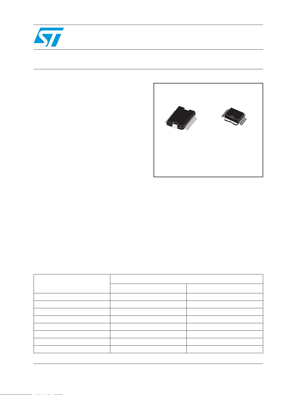
Intended for analog and digital satellite receivers,
the LNBP is a monolithic linear voltage regulator,
assembled in PowerSO-20 and PowerSO-10,
specifically designed to provide the powering
voltages and the interfacing signals to the LNB
downconverter situated in the antenna
TM
LNBP20 / LNBP1X series
10
1
PowerSO-20
via the coaxial cable. Since most satellite
receivers have two antenna ports, the output
voltage of the regulator is available at one of two
logic-selectable output pins (LNBA, LNBB). When
the IC is powered and put in Stand-by (EN pin
LOW), both regulator outputs are disabled to
allow the antenna downconverters to be
supplied/controlled by others satellite receivers
sharing the same coaxial lines. In this occurrence
the device will limit at 3 mA (max) the backward
current that could flow from LNBA and LNBB
output pins to GND. (See continuous description).
PowerSO-10
Order codes
Package
Part number
PowerSO-20 PowerSO-10
LNBP10 LNBP10SP-TR
LNBP11 LNBP11SP-TR
LNBP12 LNBP12SP-TR
LNBP13 LNBP13SP-TR
LNBP14 LNBP14SP-TR
LNBP15 LNBP15SP-TR
LNBP16 LNBP16SP-TR
LNBP20 LNBP20PD-TR
May 2007 Rev. 10 1/24
www.st.com
24

LNBP20 / LNBP1X series
Contents
1 Description (continued) . . . . . . . . . . . . . . . . . . . . . . . . . . . . . . . . . . . . . . 3
2 Pin configuration . . . . . . . . . . . . . . . . . . . . . . . . . . . . . . . . . . . . . . . . . . . 4
3 Maximum ratings . . . . . . . . . . . . . . . . . . . . . . . . . . . . . . . . . . . . . . . . . . . . 6
4 Diagram . . . . . . . . . . . . . . . . . . . . . . . . . . . . . . . . . . . . . . . . . . . . . . . . . . . 7
5 Electrical characteristics . . . . . . . . . . . . . . . . . . . . . . . . . . . . . . . . . . . . . 8
6 Typical characteristics . . . . . . . . . . . . . . . . . . . . . . . . . . . . . . . . . . . . . . 10
7 Typical application schematics . . . . . . . . . . . . . . . . . . . . . . . . . . . . . . . 14
8 Package mechanical data . . . . . . . . . . . . . . . . . . . . . . . . . . . . . . . . . . . . 18
9 Revision history . . . . . . . . . . . . . . . . . . . . . . . . . . . . . . . . . . . . . . . . . . . 23
2/24

LNBP20 / LNBP1X series Description (continued)
1 Description (continued)
For slave operation in single dish, dual receiver systems, the bypass function is
implemented by an electronic switch between the Master Input pin (MI) and the LNBA pin,
thus leaving all LNB powering and control functions to the Master Receiver. This electronic
switch is closed when the device is powered and EN pin is LOW.
The regulator outputs can be logic controlled to be 13 or 18 V (typ.) by mean of the VSEL
pin for remote controlling of LNBs. Additionally, it is possible to increment by 1V (typ.) the
selected voltage value to compensate the excess voltage drop along the coaxial cable (LLC
pin HIGH).
In order to reduce the power dissipation of the device when the lowest output voltage is
selected, the regulator has two Supply Input pins V
respectively at 16V (min) and 23V (min), and an internal switch automatically will select the
suitable supply pin according to the selected output voltage. If adequate heatsink is
provided and higher power losses are acceptable, both supply pins can be powered by the
same 23V source without affecting any other circuit performance.
The ENT (Tone Enable) pin activates the internal oscillator so that the DC output is
modulated by a ±0.3 V, 22KHz (typ.) square wave. This internal oscillator is factory trimmed
within a tolerance of ±2KHz, thus no further adjustments neither external components are
required.
CC1
and V
. They must be powered
CC2
A burst coding of the 22KHz tone can be accomplished thanks to the fast response of the
ENT input and the prompt oscillator start-up. This helps designers who want to implement
the DiSEqC
TM
protocols
(a)
.
In order to improve design flexibility and to allow implementation of newcoming LNB remote
control standards, an analogic modulation input pin is available (EXTM). An appropriate DC
blocking capacitor must be used to couple the modulating signal source to the EXTM pin.
When external modulation is not used, the relevant pin can be left open.
Two pins are dedicated to the overcurrent protection/monitoring: CEXT and OLF. The
overcurrent protection circuit works dynamically: as soon as an overload is detected in
either LNB output, the output is shut-down for a time t
determined by the capacitor
off
connected between CEXT and GND. Simultaneously the OLF pin, that is an open collector
diagnostic output flag, from HIGH IMPEDANCE state goes LOW.
After the time has elapsed, the output is resumed for a time t
=1/15t
on
(typ.) and OLF goes
off
in HIGH IMPEDANCE. If the overload is still present, the protection circuit will cycle again
through t
and ton until the overload is removed. Typical ton+t
off
value is 1200ms when a
off
4.7µF external capacitor is used.
This dynamic operation can greatly reduce the power dissipation in short circuit condition,
still ensuring excellent power-on start up even with highly capacitive loads on LNB outputs.
The device is packaged in PowerSO-20 for surface mounting. When a limited functionality in
a smaller package matches design needs, a range of cost-effective PowerSO-10 solutions
is also offered. All versions have built-in thermal protection against overheating damage.
a. External components are needed to comply to level 2.x and above (bidirectional) DiSEqCTM bus hardware
requirements. DiSEqC
TM
is a trademark or EUTELSAT.
3/24
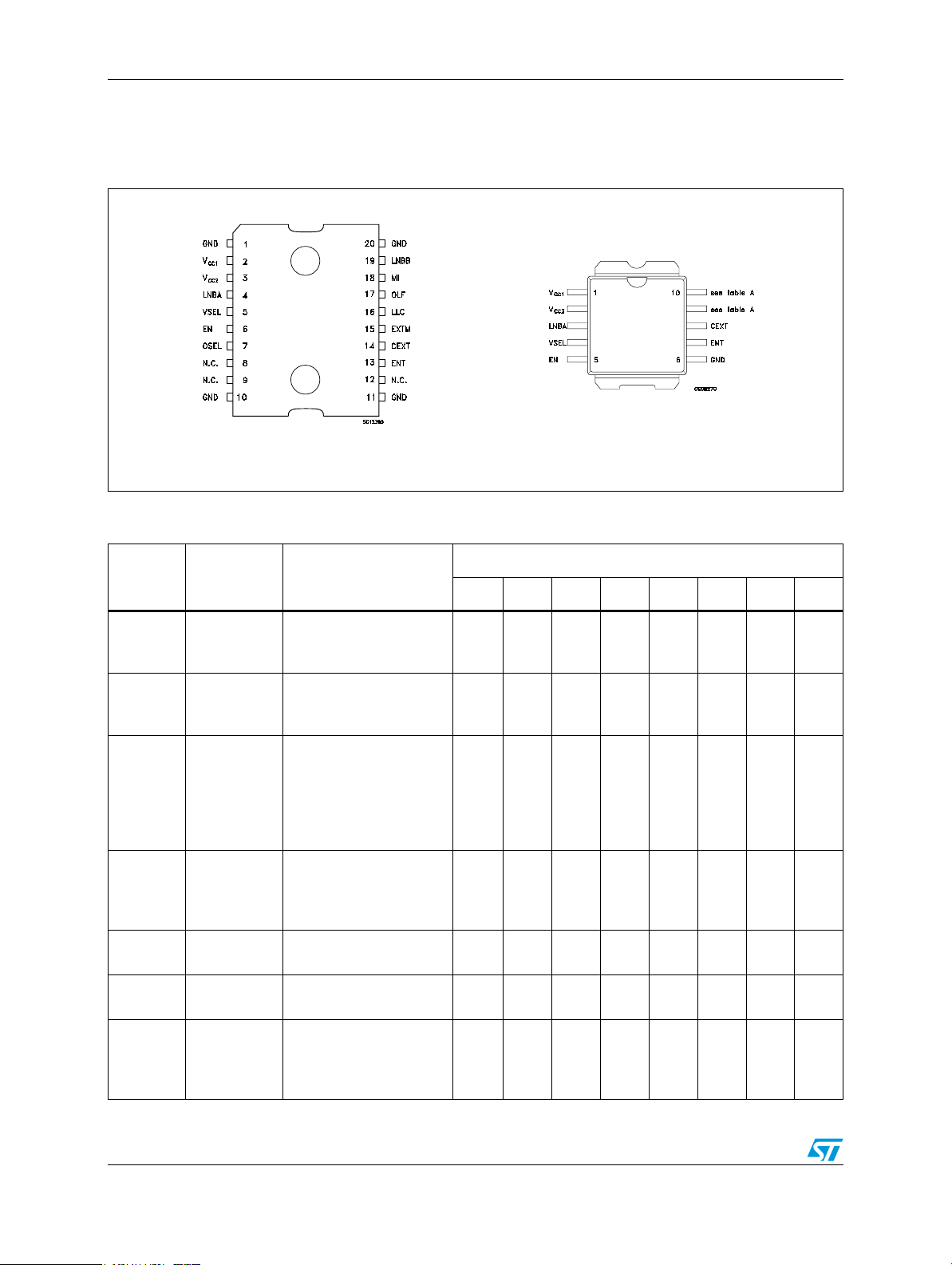
Pin configuration LNBP20 / LNBP1X series
2 Pin configuration
Figure 1. Pin connections (top view)
PowerSO-20
Table 1. Pin Description
SYMBOL NAME FUNCTION
V
V
CC1
CC2
Supply input
1
Supply input
2
LNBA Output port
Output
V
SEL
voltage
selection:13
or 18V (typ)
EN Port enable
15V to 25V supply. It is
automatically selected
when V
= 13 or 14V
OUT
22V to 25V supply. It is
automatically selected
when V
= 18 or 19V
OUT
See truth table voltage
and port selection. In
stand-by mode this port
is powered by the MI pin
via the internal bypass
switch
Logic control input: see
truth table
Logic control input: see
truth table
PowerSO-10
PIN NUMBER vs SALES TYPE (LNBP)
20PD 10SP 11SP 12SP 13SP 14SP 15SP 16SP
2111 111
32222222
43333333
54444444
65555555
OSEL Port selection
GND Ground
4/24
Logic control input: see
truth table
Circuit ground. It is
internally connected to
the die frame
7 9 NA NA NA NA NA NA
1
10
11
6666666
20

LNBP20 / LNBP1X series Pin configuration
Table 1. Pin Description
PIN NUMBER vs SALES TYPE (LNBP)
SYMBOL NAME FUNCTION
20PD 10SP 11SP 12SP 13SP 14SP 15SP 16SP
ENT
CEXT
EXTM
LLC
OLF
MI Master input
22KHz tone
enable
External
capacitor
External
modulator
Line length
compens.
(1V typ)
Over load
flag
Logic control input: see
truth table
Timing capacitor used by
the dynamic overload
protection. Typical
application is 4.7μF for a
1200ms cycle
External modulation
input. Needs DC
decoupling to the AC
source. if not used, can
be left open.
Logic control input: see
truth table
Logic output (open
collector). Normally in
HIGH IMPEDANCE,
goes LOW when current
or thermal overload
occurs
In stand-by mode, the
voltage on MI is routed to
LNBA pin. Can be left
open if bypass function is
not needed
137777777
148888888
15 NA NA NA 9 NA 9 9
16 NA NA 9 NA 9 NA 10
17 NA 9 NA NA 10 10 NA
18 NA 10 10 10 NA NA NA
See truth tables for
LNBB Output port
voltage and port
selection
19 10 NA NA NA NA NA NA
Note: The limited pin availability of the PowerSO-10 package leads to drop some functions.
5/24
Maximum ratings LNBP20 / LNBP1X series
3 Maximum ratings
Table 2. Absolute maximum ratings
Symbol Parameter Value Unit
V
V
I
O
V
I
SW
P
T
stg
T
op
DC Input voltage (V
I
Output voltage -0.3 to 28 V
O
CC1
, V
, MI) 28 V
CC2
Output current (LNBA, LNBB) Internally Limited mA
Logic input voltage (ENT, EN OSEL, VSEL, LLC) -0.5 to 7 V
I
Bypass switch current 900 mA
Power dissipation at T
D
< 85°C 14 W
case
Storage temperature range -40 to +150 °C
Operating junction temperature range -40 to +125 °C
Note: Absolute Maximum Ratings are those values beyond which damage to the device may
occur. Functional operation under these condition is not implied
Table 3. Thermal data
Symbol Parameter PowerSO-20 PowerSO-10 Unit
R
thJC
Table 4. Logic Controls Truth Table
Thermal resistance junction-case 2 2 °C/W
CONTROL I/O PIN NAME L H
OUT OLF I
OUT
> I
or Tj > 150°C I
OMAX
OUT
< I
IN ENT 22KHz tone OFF 22KHz tone ON
IN EN See Table Below See Table Below
IN OSEL See Table Below See Table Below
IN VSEL See Table Below See Table Below
IN LLC See Table Below See Table Below
OMAX
EN OSEL VSEL LLCO V
LXXXV
LNBA
- 0.4V (typ.) Disabled
MI
H L L L 13V (typ.) Disabled
H L H L 18V (typ.) Disabled
H L L H 14V (typ.) Disabled
H L H H 19V (typ.) Disabled
H H L L Disabled 13V (typ.)
H H H L Disabled 18V (typ.)
H H L H Disabled 14V (typ.)
H H H H Disabled 19V (typ.)
Note: All logic input pins have internal pull-down resistor (typ. = 250KW)
6/24
V
LNBB
LNBP20 / LNBP1X series Diagram
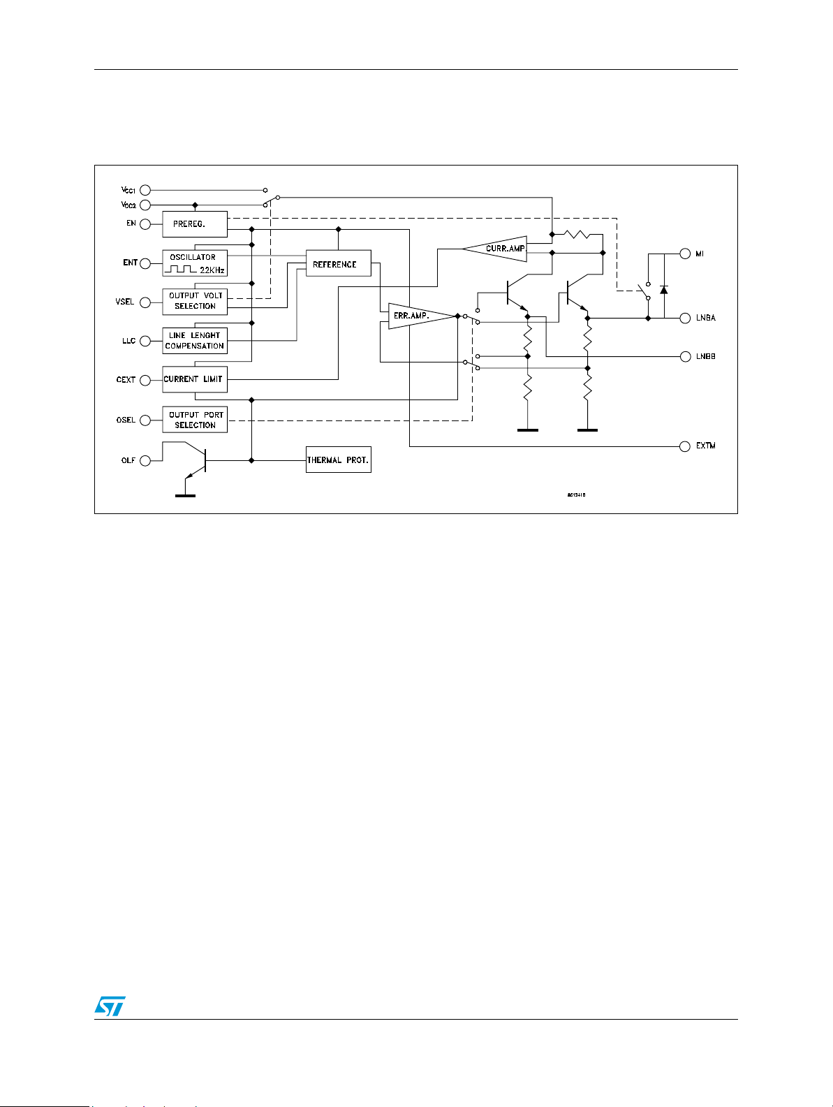
4 Diagram
Figure 2. Block diagram
7/24
Electrical characteristics LNBP20 / LNBP1X series
5 Electrical characteristics
Table 5. Electrical characteristics for LNBP Series (TJ = 0 to 85°C, CI = 0.22µF, CO = 0.1µF,
EN=H, ENT=L, LLC=L, V
Symbol Parameter Test conditions Min. Typ. Max. Unit
V
V
V
V
ΔV
ΔV
SVR Supply voltage rejection V
I
MAX
t
t
f
TONE
A
TONE
D
TONE
t
G
EXTM
V
EXTM
V
IN1
IN2
O1
O2
O
O
Supply voltage
CC1
V
Supply voltage
CC2
Output voltage
Output voltage
Line regulation
Load regulation
Output current limiting 500 650 800 mA
Dynamic overload
OFF
protection OFF time
Dynamic overload
ON
protection ON time
Tone frequency ENT=H 20 22 24 KHz
Tone amplitude ENT=H 0.55 0.72 0.9 V
Tone duty cycle ENT=H 40 50 60 %
, tfTone rise and fall time ENT=H 5 10 15 µs
r
External modulation gain ΔV
External modulation input
voltage
=16V, V
IN1
I
= 500 mA, ENT=H, VSEL=L, LLC=L 15 25 V
O
= 500 mA, ENT=H, VSEL=L, LLC=H 16 25 V
I
O
I
= 500 mA, ENT=H, VSEL=L, LLC=L 22 25 V
O
= 500 mA, VSEL=L, LLC=H 23 25 V
I
O
I
= 500 mA, VSEL=H, LLC=L 17.3 18 18.7 V
O
I
= 500 mA, VSEL=H, LLC=H 19 V
O
I
= 500 mA, VSEL=L, LLC=L 12.5 13 13.5 V
O
= 500 mA, VSEL=L, LLC=H 14 V
I
O
V
=15 to 18V, V
IN1
=22 to 25V, V
V
IN2
= V
=22V, V
IN2
V
IN1=VIN2
= 50 to 500mA
I
O
IN1
Output Shorted, C
Output Shorted, C
/ΔV
OUT
EXTM
IN2
=23V I
OUT
OUT
OUT
=50mA, unless otherwise specified.)
OUT
=13V 4 40 mV
=18V 4 40 mV
=13 or 18V
80 180 mV
= 23 ± 0.5Vac, fac = 120 Hz, 45 dB
= 4.7µF 1100 ms
EXT
= 4.7µF t
EXT
/15 ms
OFF
, f = 10Hz to 40KHz 5
AC Coupling 400 mV
PP
PP
Z
8/24
EXTM
V
SW
V
OL
I
OZ
V
IL
External modulation
impedance
Bypass switch voltage
drop (MI to LNBA)
Overload flag pin logic
LOW
Overload flag pin OFF
state leakage current
Control input pin logic
LOW
f = 10Hz to 40KHz 400 Ω
EN=L, I
I
=8mA 0.28 0.5 V
OL
V
OH
=300mA, V
SW
CC2-VMI
= 6V 10 µA
=4V 0.35 0.6 V
0.8 V
 Loading...