

ST LNBP8L, LNBP9L, LNBP10L, LNBP11L User Manual
LNB supply and control voltage regulator
Features
■ Simplest integrated solution for LNB remote
supply and control
■ 500 mA guaranteed output current
■ Dual input supply for reducing power
dissipation (DFN package)
■ 3-state function to enable/disable and select
the output voltage level through a single pin
■ Fast oscillator startup for DiSEq™ encoding
(LNBP9L/11L versions)
■ External 22 kHz modulation input pin
(LNBP8L/10L versions)
■ Cable length compensation, LLC pin
(LNBP10L, LNBP11L versions)
■ Short-circuit and over-temperature protection
■ LNB overload and short-circuit dynamic
protection (LNBP10L, LNBP11L versions)
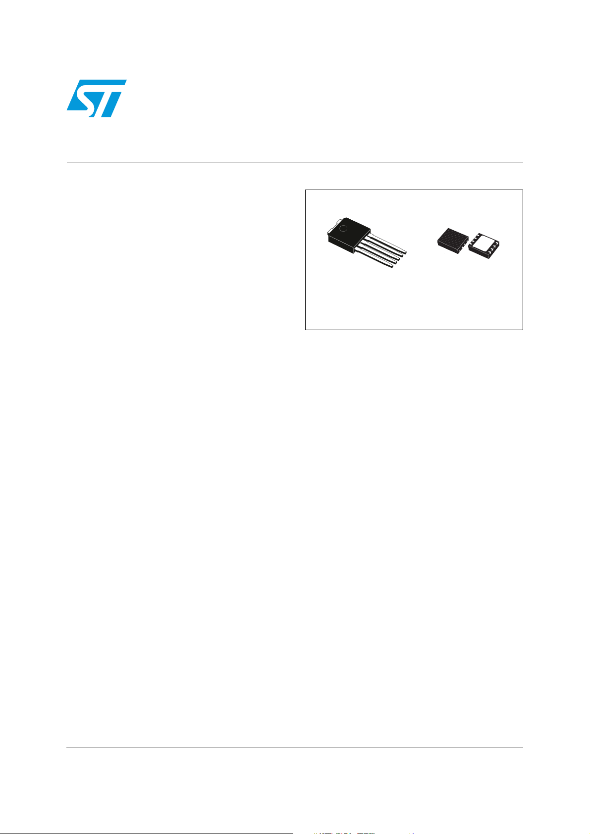
■ Available in DFN8 (5 x 6 mm) and IPPAK
packages
Description
Intended for analog and digital satellite receivers,
the LNBP is a monolithic linear voltage regulator,
assembled in the DFN8 (5 x 6) and IPPAK
packages, specifically designed to provide the
powering voltages and the interfacing signals to
the LNB down-converter. The regulator output
can be logic controlled for 13 V or 18 V (typ.) by
means of the EN/VSEL 3-state pin for remotely
controlling the LNB. When the IC is powered and
put in standby (EN/VSEL pin at high impedance),
the regulator output is disabled. In order to reduce
power dissipation, the LNBP10L/11L versions (on
DFN package) feature 2 supply inputs: V
V
. These pins must be powered, respectively,
CC2
at 15 V (min.) and 22 V (min.), and an internal
switch will automatically select the appropriate
supply voltage according to the selected output
voltage. The LNBP8L/9L versions (in the IPPAK
package) have only one supply input pin, which
CC1
and
LNBP8L, LNBP9L
LNBP10L, LNBP11L
IPPAK
must be supplied at 22 V (min.). Additionally, the
LNBP10L/11L versions have the LLC pin to
increment the selected output voltage value by 1
V (typ.) to compensate for the excess voltage
drop along the coaxial cable (LLC pin HIGH). An
analog 22 kHz modulation input pin (EXTM) is
available in the LNBP8L and LNBP10L versions.
An appropriate DC blocking capacitor must be
used to couple the modulating signal source to
the EXTM pin. The LNBP10L/11L versions are
also equipped with over-current dynamic
protection: as soon as an overload is detected the
output is shut down for the time T
determined by the capacitor connected between
the CEXT pin and GND. After the time has
elapsed, the output is resumed for a time T
(1/12)*T
(typ.). If the overload is still present,
OFF
the protection circuit will cycle again through T
and T
T
ON+TOFF
until the overload is removed. A typical
ON
value is 1100 ms when a 4.7 µF
external capacitor is used on the C
dynamic operation can greatly reduce the power
dissipation in short-circuit condition, while
ensuring excellent power-on startup even with
highly capacitive loads on the LNB outputs. The
device is packaged in the IPPAK for through-hole
mounting and in the DFN8 (5 x 6) for surface
mounting. Both package solutions are offered in
two versions: with ten pins (LNBP9L/11L) to use
with the integrated 22 kHz tone generator, or with
the EXTM pin (LNBP8L/10L) to use external 22
kHz sources. All versions have built-in thermal
protection to prevent overheating damage.
DFN8 (5 x 6 mm)
which is
OFF,
ON
. This
EXT
=
OFF
August 2010 Doc ID 15153 Rev 2 1/21
www.st.com
21

Contents LNBP8L, LNBP9L, LNBP10L, LNBP11L
Contents
1 Diagram . . . . . . . . . . . . . . . . . . . . . . . . . . . . . . . . . . . . . . . . . . . . . . . . . . . 3
2 Pin configuration . . . . . . . . . . . . . . . . . . . . . . . . . . . . . . . . . . . . . . . . . . . . 4
3 Maximum ratings . . . . . . . . . . . . . . . . . . . . . . . . . . . . . . . . . . . . . . . . . . . . 5
4 Electrical characteristics . . . . . . . . . . . . . . . . . . . . . . . . . . . . . . . . . . . . . 6
5 Typical application circuits . . . . . . . . . . . . . . . . . . . . . . . . . . . . . . . . . . . 8
6 Detailed description and application hints . . . . . . . . . . . . . . . . . . . . . . . 9
6.1 Input voltage protection . . . . . . . . . . . . . . . . . . . . . . . . . . . . . . . . . . . . . . 10
6.2 Single supply for the DFN package . . . . . . . . . . . . . . . . . . . . . . . . . . . . . 10
6.3 IPPAK mounting and thermal considerations . . . . . . . . . . . . . . . . . . . . . . 11
7 Typical performance characteristics . . . . . . . . . . . . . . . . . . . . . . . . . . . 13
8 Package mechanical data . . . . . . . . . . . . . . . . . . . . . . . . . . . . . . . . . . . . 16
9 Ordering information . . . . . . . . . . . . . . . . . . . . . . . . . . . . . . . . . . . . . . . 19
10 Revision history . . . . . . . . . . . . . . . . . . . . . . . . . . . . . . . . . . . . . . . . . . . 20
2/21 Doc ID 15153 Rev 2
LNBP8L, LNBP9L, LNBP10L, LNBP11L Diagram
1 Diagram
Figure 1. Block diagram
VCC1
VCC1
VCC1
VCC1
VCC2
VCC2
VCC2
VCC2
R
R
R
R
SENSE
SENSE
SENSE
EN/VSEL
EN/VSEL
EN/VSEL
EN/VSEL
LLC
LLC
LLC
LLC
CEXT
CEXT
CEXT
CEXT
TEN
TEN
TEN
TEN
TRISTATE ENABLE &
TRISTATE ENABLE &
TRISTATE ENABLE &
TRISTATE ENABLE &
VOUT SELECTION
VOUT SELECTION
VOUT SELECTION
VOUT SELECTION
DYNAMIC
DYNAMIC
DYNAMIC
DYNAMIC
CURRENT LIMIT
CURRENT LIMIT
CURRENT LIMIT
CURRENT LIMIT
22KHz
22kHz
22KHz
22kHz
OSCILLATOR
OSCILLATOR
OSCILLATOR
OSCILLATOR
VOLTAGE
VOLTAGE
VOLTAGE
VOLTAGE
VOLTAGE
VOLTAGE
REFERENCE
REFERENCE
REFERENCE
REFERENCE
REFERENCE
REFERENCE
THERMAL
THERMAL
THERMAL
THERMAL
PROTECTION
PROTECTION
PROTECTION
PROTECTION
SENSE
OUTPUT
OUTPUT
OUTPUT
OUTPUT
EXTM
EXTM
EXTM
EXTM
LNBP8L/9L/10L/11L
LNBP8L/9L/10L/11L
LNBP8L/9L/10L/11L
LNBP8L/9L/10L/11L
GND
GND
GND
GND
Doc ID 15153 Rev 2 3/21
Pin configuration LNBP8L, LNBP9L, LNBP10L, LNBP11L
2 Pin configuration
Figure 2. Pin connections (top view for IPPAK, bottom view for DFN8)
IPPAK
Table 1. Pin description
Pin n° (DFN)
LNBP10/11L
1-
21
32OUTPUT
4, ePAD 3, ePAD GROUND GROUND
64EN/VSEL
55EXTM/TEN
Pin n°
(IPPAK)
LNBP8/9L
Name Pin function
VCC1
(not available for
IPPAK)
VCC2
pin for
(V
CC
IPPAK)
Supply input 1: 15 V to 25 V supply. For DFN package it is
automatically selected when V
V
supplied at 22 V min.
Supply input 2: 22 V to 25 V supply. For DFN package it is
automatically selected when V
V
supplied at 22 V min.
Output: regulator output. It is 13 V typ when EN/VSEL LOW and
18 V typ when EN/VSEL HIGH.
Enable and output voltage selection 3-state pin: logic control
input 3-state pin for the remote controlling of the LNB; if LOW
V
IC is set in shut down mode (V
Tone enable (LNBP9-11): logic control input to enable internal
tone generator.
External modulation (LNBP8-10): Needs DC decoupling to the
AC source. If not used can be left floating.
and V
CC1
and V
CC1
= 13 V, when HIGH V
OUT
are internally connected together to pin 1 to be
CC2
are internally connected together to the pin 1 to be
CC2
DFN8 (5 x 6 mm)
= 13 V. For IPPAK package
OUT
= 18 V. For IPPAK package
OUT
= 18 V, if left at high impedance the
OUT
OUT
= 0 V)
8 NA LLC LLC: logic control input to add 1 V typ.
C
: timing capacitor used by the dynamic overload protection.
7NAC
EXT
EXT
Typical application is 4.7 µF for a 1100 ms cycle
4/21 Doc ID 15153 Rev 2
LNBP8L, LNBP9L, LNBP10L, LNBP11L Maximum ratings
3 Maximum ratings
Table 2. Absolute maximum ratings
Symbol Parameter Value Unit
VCC1, VCC2 Input voltages -0.3 to 28 V
VCC1-OUTPUT VCC1 voltage with respect to OUTPUT voltage
VCC2-OUTPUT VCC2 voltage with respect to OUTPUT voltage
EN/VSEL, TEN,
LLC
EXTM External modulation input voltage -0.3 to 1 V
OUTPUT Output voltage -0.3 to 25 V
T
STG
ESD
DFN package
Logic input voltage -0.3 to 7 V
Storage temperature range -50 to 150 °C
ESD rating with human body model (HBM) for all pins except 1, 2, 6 2 kV
ESD rating with human body model (HBM) for pins 1, 2, 6 1.5
(1)
(1)
-0.3 to 25 V
-0.3 to 25 V
ESD
IPPAK package
1. Exposure beyond the VCC1 and VCC2 with respect to OUTPUT absolute-maximum-rated voltages during OUTPUT pin
overload or short-circuit to GROUND may cause permanent damage to the device.
ESD rating with human body model (HBM) for all pins except 1, 4 2 kV
ESD rating with human body model (HBM) for pins 1, 4 1.5
Note: Absolute maximum ratings are those values beyond which damage to the device may occur.
These are stress ratings only and functional operation of the device at these conditions is
not implied. Exposure to absolute-maximum-rated conditions for extended periods may
affect device reliability. All voltage values are with respect to network ground terminal unless
otherwise stated.
Table 3. Operating ratings
Symbol Parameter Value Unit
T
J
VCC1 Input voltage 15 to 25 V
VCC2 Input voltage 22 to 25 V
Operating junction temperature range 0 to 125 °C
Table 4. Thermal data
Symbol Parameter IPPAK DFN8 Unit
R
R
Thermal resistance junction-ambient
thJA
Thermal resistance junction-case 8 °C/W
thJC
Doc ID 15153 Rev 2 5/21
(mounted on PCB 2s2p)
35
°C/W
Electrical characteristics LNBP8L, LNBP9L, LNBP10L, LNBP11L
4 Electrical characteristics
Refer to the typical application circuits in Figure 3 and Figure 4, V
V
= 23 V
CC2
T
= 0 °C to 85 °C, unless otherwise stated. Typical values are referred to TJ = 25 °C.
J
Table 5. Electrical characteristics
(1)
, EN/VSEL = LOW, TEN = LLC = LOW, EXTM = FLOATING, I
CC1
= 16 V,
OUT
= 50 mA,
Symbol Parameter Test conditions Min. Typ. Max. Unit
I
= 500 mA, TEN=HIGH,
V
V
V
ΔV
ΔV
I
F
A
D
G
V
Z
CC1
CC2
OUT
OUT
OUT
MAX
TONE
TONE
TONE
, t
t
r
EXTM
EXTM
EXTM
OUT
VCC supply input 1
(1)
EN/VSEL=LOW, LLC=LOW
I
= 500 mA, TEN=HIGH,
OUT
EN/VSEL=LOW, LLC= HIGH
I
= 500 mA, TONE=HIGH,
OUT
VCC supply input 2
(1)
EN/VSEL=HIGH, LLC=LOW
= 500 mA, TONE=HIGH,
I
OUT
EN/VSEL=HIGH, LLC= HIGH
I
= 500 mA, EN/VSEL=LOW 12.5 13.25 14 V
OUT
= 500 mA, EN/VSEL=HIGH 17 18 19 V
I
OUT
Output voltage
Line regulation
Load regulation
(1)
I
= 500 mA, EN/VSEL=LOW,
OUT
LLC=HIGH
I
OUT
V
CC1
(2)
= 500 mA, EN/VSEL=LLC=HIGH
from 15 V to 18 V, EN/VSEL=LOW
or HIGH
V
CC1
= V
CC2
= 22 V, I
from 50 mA to
OUT
500 mA, EN/VSEL=LOW or HIGH
Output current limiting 550 700 850 mA
Tone frequency TEN=High 20 22 24 kHz
Tone amplitude TEN=High 0.4 0.65 0.9 V
Tone duty cycle TEN=High 40 50 60 %
/Δ V
(3)
, freq. from 10 kHz to 40
EXTM
Tone Rise and Fall Time TEN=High
f
External modulation Gain
External modulation input
voltage
External modulation
impedance
Δ V
OUT
kHz
AC Coupling 400 mV
Freq. from 10 kHz to 40 kHz 400 Ω
15 25
16 25
22 25
23 25
14.25 V
(2)
19 V
540mV
50 150 mV
51015µs
4.5 5.5 6.5
V
V
PP
PP
V
ILT
V
IHT
I
IHT
Control input logic LOW
threshold for 3-state pin
Control input logic HIGH
threshold for 3-state pin
3-state control pin input
current HIGH
EN/VSEL 0.8 1 1.2 V
EN/VSEL 1.8 2 2.2 V
V
= 5 V, EN/VSEL -400 µA
IHT
6/21 Doc ID 15153 Rev 2
LNBP8L, LNBP9L, LNBP10L, LNBP11L Electrical characteristics
Table 5. Electrical characteristics (continued)
Symbol Parameter Test conditions Min. Typ. Max. Unit
I
ILT
V
V
I
IH
I
CC
T
OFF
T
ON
I
OBK
T
SHDN
ΔT
SHDN
1. For IPPAK package V
25 V
2. Only DFN package
3. Guaranteed by design
3-state control pin input
current LOW
Control input logic LOW TEN, LLC 0.8 V
IL
Control input logic HIGH TEN, LLC 2.5 V
IH
Control pins input current V
Supply current
Dynamic overload
protection OFF time
Dynamic overload
protection ON time
Output backward current Output forced to 21 V 6 mA
Thermal shutdown
threshold
Thermal shutdown
hysteresis
CC1
and V
= 0 V, EN/VSEL +180 µA
V
ILT
= 5 V, TEN, LLC 20 µA
IH
Output disabled EN/VSEL=High
impedance (floating)
Output enabled EN/VSEL=HIGH,
TEN=HIGH, I
Output shorted, C
Output shorted, C
OUT
= 500 mA
= 4.7 µF
EXT
= 4.7 µF
EXT
(2)
(2)
1.7 2.4 mA
3.7 6.3 mA
1000 ms
T
OFF
/12
165 °C
25 °C
are internally connected to the pin 1 (VCC) to be supplied in the range from 22 V up to
CC2
ms
Doc ID 15153 Rev 2 7/21
 Loading...