

查询LMV358IYD供应商
Features
■ Operating range from V
■ Rail-to-rail input and output
■ Extended V
(VDD - 0.2 V to VCC + 0.2 V)
icm
■ Low supply current (145 µA)
■ Gain bandwidth product (1 MHz)
■ ESD tolerance (2 kV)
■ Latch-up immunity
■ Available in SOT23-5 micropackage
= 2.7 V to 6 V
CC
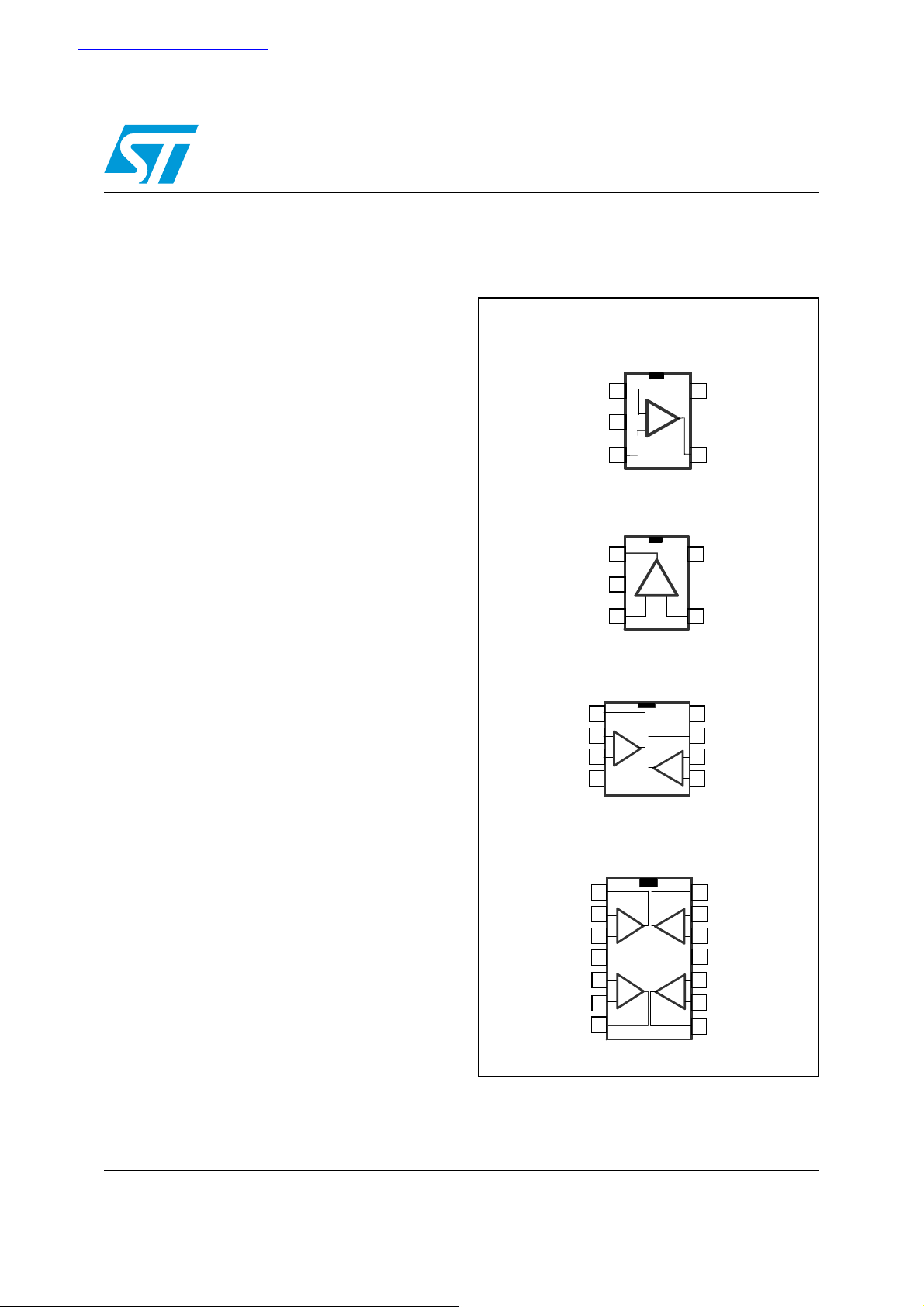
LMV321-LMV358-LMV324
Low cost low power input/output rail-to-rail
operational amplifiers
LMV321ILT
(SOT23-5)
Non Inverting Input
Non Inverting Input
Non Inverting Input
VDD
VDD
VDD
Inverting Input
Inverting Input
Inverting Input
1
1
1
2
2
2
3
3
3
LMV321RILT
(SOT23-5)
5
5
5
VCC
VCC
VCC
+
+
_
_
Output
Output
Output
4
4
4
Applications
■ Two-cell battery-powered systems
■ Battery-powered electronic equipment
■ Cordless phones
■ Personal medical care (glucose meter)
■ Laptops
■ PDAs
Description
The LMV321/358/324 family (single, dual and
quad) answers the need for low cost, general
purpose operational amplifiers. They oper ate with
voltages as low as 2.7 V and feature both input
and output rail-to-rail, 145 µA con sumption
current and 1 MHz gain bandwidth product
(GBP).
With a such low consumption and a sufficient
GBP for many applications, these op-amps are
very well-suited for any kind of battery-supplied
and portable equipment ap plic ation.
The LMV321 is housed in the space-saving 5-pin
SOT23-5 package which simplifies the board
design (overall dimensio ns are 2.8 mm x 2.9 mm).
The SOT23-5 has two pinning configurations to
answer all application requirements.
VCC
Output
Output
Non Inverting Input Inverting Input
Non Inverting Input Inverting Input
VDD
VDD
1
1
2
2
3
3
VCC
5
5
4
4
LMV358ID/IDT-LMV358IPT
(SO-8, TSSOP-8)
Output 1
Output 1
Inverting Input 1
Inverting Input 1
Non Inverting Input 1
Non Inverting Input 1
VDD
VDD
1
1
_
_
2
2
+
+
3
3
4
4
VCC
VCC
8
8
7
7
Output 2
Output 2
_
_
Inverting Input 2
Inverting Input 2
6
6
+
+
Non Inverting Input 2
Non Inverting Input 2
5
5
LMV324ID/IDT-LMV324IPT
(SO-14, TSSOP-14)
Output 4
Output 1
Output 1
Inverting Input 1
Inverting Input 1
Non Inverting Input 1
Non Inverting Input 1
Non Inverting Input 2
Non Inverting Input 2
Inverting Input 2
Inverting Input 2
Output 2
Output 2
VCC
VCC
1
1
_
_
2
2
+
+
3
3
4
4
5
5
+
+
_
_
6
6
7
7
Output 4
14
14
_
_
13
13
Inverting Input 4
Inverting Input 4
+
+
Non Inverting Input 4
Non Inverting Input 4
12
12
VDD
VDD
11
11
10
10
Non Inverting Input 3
Non Inverting Input 3
+
+
_
_
Inverting Input 3
Inverting Input 3
9
9
Output 3
Output 3
8
8
February 2008 Rev 3 1/14
www.st.com
14
Absolute maximum ratings and operating conditions LMV321-LMV358-LMV324
1 Absolute maximum ratings and operating conditions
Table 1. Absolute maximum ratings
Symbol Parameter Value Unit
V
T
T
V
V
oper
T
Supply voltage
CC
Differential input voltage
id
Input voltage VDD-0.3 to VCC+0.3 V
in
Operating free air temperature range -40 to + 125 °C
Storage temperature -65 to +150 °C
stg
Maximum junction temperature 150 °C
j
Thermal resistance junction to ambient
SOT23-5
R
thja
SO-8
SO-14
TSSOP8
TSSOP14
Thermal resistance junction to case
SOT23-5
R
thjc
SO-8
SO-14
TSSOP8
TSSOP14
HBM: human body model
ESD
MM: machine model
CDM: charged device model
Lead temperature (soldering, 10sec) 250 °C
Output short-circuit duration see note
1. All voltage values, except differential voltage are with respect to network terminal.
2. Differential voltages are the non-inverting input terminal with respect to the inverting input terminal. If
V
> ±1 V, the maximum input current must not exceed ±1 mA. In this case (Vid > ±1 V), an input series
id
resistor must be added to limit input current.
3. Short-circuits can cause excessive heating. Destructive dissipation can result from simultaneous shortcircuits on all amplifiers. All values are typical.
4. Human body model: A 100 pF capacitor is charged to the specified voltage, then discharged through a
1.5 k
Ω resistor between two pins of the device. This is done for all couples of connected pin combinations
while the other pins are floating.
5. Machine model: A 200pF capacitor is charged to the specified voltage, then discharged directly between
two pins of the device with no external series resistor (internal resistor < 5
connected pin combinations while the other pins are floating.
6. Charged device model: all pins and the package are charged together to the specified voltage and then
discharged directly to the ground through only one pin. This is done for all pins.
No value specified for CDM on SOT23-5L package. The value is given for SO and TSSOP packages.
7. Short-circuits from the output to V
approximately 48 mA, independent of the magnitude of V
simultaneous short-circuits on all amplifiers.
(1)
7V
(2)
(3)
±1 V
250
125
103
120
100
(3)
81
40
31
37
32
(4)
(5)
(6)
can cause excessive heating. The maximum output current is
CC
. Destructive dissipation can result from
CC
2kV
200 V
1.5 kV
(7)
Ω). This is done for all couples of
°C/W
°C/W
2/14

LMV321-LMV358-LMV324 Absolute maximum ratings and operating conditions
Table 2. Operating conditions
Symbol Parameter Value Unit
V
CC
V
icm
V
icm
T
oper
1. At 25°C, for 2.7 ≤ VCC ≤ 6V, V
2. In full temperature range, both rails can be reached when VCC does not exceed 5.5 V.
Supply voltage 2.7 to 6 V
Common mode input voltage range
Common mode input voltage range
(1)
(2)
VDD -0.2 to VCC + 0.2 V
VDD to V
CC
Operating free air temperature range -40 to + 125 °C
is extended to VDD - 0.2 V, VCC + 0.2 V.
icm
V
3/14
Electrical characteristics LMV321-LMV358-LMV324
2 Electrical characteristics
Table 3. VCC = +2.7V, VDD = 0V, C
connected to VCC/2, T
L & RL
= 25°C (unless otherwise specified)
amb
Symbol Parameter Conditions Min. Typ. Max. Unit
V
= V
V
ΔV
Input offset voltage
io
Input offset voltage drift 2 µV/°C
io
I
Input offset current
io
Input bias current
I
ib
icm
T
min
V
icm
T
min
V
icm
T
min
CMR Common mode rejection ratio 0 ≤ V
SVR Supply voltage rejection ratio V
A
Large signal voltage gain
vd
icm
V
out
R
RL = 2kΩ
V
= 100mV
id
T
V
High level output voltage
OH
min
RL = 10kΩ
RL = 2kΩ
V
= -100mV
id
T
V
Low level output voltage
OL
min
RL = 10kΩ
R
= VCC/2
out
≤ T
≤ T
amb
max
= V
≤ T
= V
≤ T
icm
= VCC/2
out
≤ T
amb
= VCC/2
out
≤ T
amb
≤ V
CC
(1)
max
(1)
max
55 85 dB
= VCC/2 70 80 dB
= 0.5V to 2.2V
= 10kΩ
L
≤ T
amb
≤ T
max
8070100
2.6
2.55
≤ T
≤ T
amb
max
= 2kΩ
L
0.1 3
6
19
25
10 50
85
88
2.65
2.6
15
50
90
100
Output source current
I
Output current
o
I
Supply current (per amplifier)
CC
GBP Gain bandwidth product
SR Slew rate
φm Phase margin R
= 100mV, VO = V
id
DD
Output sink current
= -100mV, VO = V
V
id
= VCC/2
V
out
= 1, no load
A
VCL
T
≤ T
amb
≤ T
max
min
= 10kΩ, CL = 100pF,
R
L
CC
f = 100kHz
= 600Ω, CL = 100pF,
R
L
= 1
A
V
= 600Ω, CL = 100pF 44 Degrees
L
5
5
46
46
145 200
1MHz
0.35 V/µs
230
V
en Input voltage noise 40 nV/√Hz
THD Total harmonic distortion 0.01 %
1. Maximum values include unavoidable inaccuracies of the industrial tests.
mV
nA
nA
dB
V
mV
mA
µA
4/14
LMV321-LMV358-LMV324 Electrical characteristics
Table 4. VCC = +5V, VDD = 0V, C
connected to VCC/2, T
L & RL
= 25°C (unless otherwise specified)
amb
Symbol Parameter Conditions Min. Typ. Max. Unit
V
= V
V
ΔV
Input offset voltage
io
Input offset voltage drift 2 µV/°C
io
Input offset current
I
io
I
Input bias current
ib
icm
T
min
V
icm
T
min
V
icm
T
min
CMR Common mode rejection ratio 0 ≤ V
SVR Supply voltage rejection ratio V
A
Large signal voltage gain
vd
icm
V
out
R
RL = 2kΩ
= VCC/2
out
≤ T
≤ T
amb
max
= V
≤ T
= V
≤ T
icm
= VCC/2
out
≤ T
amb
= VCC/2
out
≤ T
amb
≤ V
CC
(1)
max
(1)
max
65 95 dB
= VCC/2 70 90 dB
= 0.5V to 4.5V
= 10kΩ
L
85
77
0.1 3
6
19
25
16 63
95
97
93
Vid = 100mV
≤ T
≤ T
amb
amb
≤ T
≤ T
max
max
4.85
4.8
4.95
4.91
40
80
180
200
T
V
High level output voltage
OH
min
RL = 10kΩ
RL = 2kΩ
V
= -100mV
id
T
V
Low level output voltage
OL
min
RL = 10kΩ
RL = 2kΩ
Output source current
I
Output current
o
I
Supply current (per amplifier)
CC
GBP Gain bandwidth product
SR Slew rate
φm Phase margin R
Vid = 100mV, VO = V
DD
Output sink current
Vid = -100mV, VO = V
= VCC/2
V
out
= 1, no load
A
VCL
T
≤ T
amb
≤ T
max
min
= 10kΩ, CL = 100pF,
R
L
CC
f = 100kHz
= 600Ω, CL = 100pF,
R
L
A
= 1
V
= 600Ω, CL = 100pF 48 Degrees
L
7
7
48
48
162 220
1.3 MHz
0.45 V/µs
250
en Input voltage noise 40 nV/√Hz
THD Total harmonic distortion 0.01 %
1. Maximum values include unavoidable inaccuracies of the industrial tests.
mV
nA
nA
dB
V
mV
mA
µA
5/14

Electrical characteristics LMV321-LMV358-LMV324
pp
Figure 1. Supply current/amplifier vs. supply
Figure 2. Input bias current vs. temperature
voltage
200
150
Tamb = 25°C
100
50
Supply Current (µA)
0
02468
Supply Voltage (V)
0
Vcc = 3V
-2
Vicm = 1.5V
-4
-6
-8
-10
Input bias current (nA)
-12
-40
-20
0
20
40
60
80
100
120
Temperature (°C)
Figure 3. Input bias current vs. temperature Figure 4. Common mode rejection vs.
temperature
0
Vcc = 5V
-2
Vicm = 2.5V
-4
-6
-8
110
Vcc = 3V
100
90
80
140
Input bias current (nA)
-10
-12
-40
-20
0
20
40
60
80
100
Temperature (°C)
Figure 5. Common mode rejection vs.
temperature
110
Vcc = 5V
100
90
80
70
Common Mode Rejection (dB)
60
-40
-20
0
40
20
Temperature (°C)
80
60
100
120
120
140
140
70
Common Mode Rejection (dB)
60
-50
0
50
100
Temperature (°C)
Figure 6. Supply voltage rejection vs.
temperature
110
Vcc = 5V
Vicm = 2.5V
100
90
80
70
Supply Voltage Rejection (dB)
60
-40
-20
0
40
20
Temperature (°C)
80
60
100
120
150
140
6/14

LMV321-LMV358-LMV324 Electrical characteristics
)
Figure 7. Open loop gain vs. temperature Figure 8. Open loop gain vs. temperature
110
Vcc = 3V
100
RL = 10 kohms
RL = 2 kohms
90
80
Open Loop Gain (dB)
70
-40
-20
0
40
20
80
60
100
120
Temperature (°C)
Figure 9. Supply voltage rejection vs.
140
110
VCC = 5V
100
RL = 10 kohms
RL = 2 kohms
90
80
Open Loop Gain (dB)
70
-40
-20
0
40
20
80
60
100
120
Temperature (°C)
Figure 10. Output current vs. output voltage
temperature
110
Vcc = 3V
Vicm = 1.5V
100
90
80
70
Supply Voltage Rejection (dB)
60
-40
-20
0
20
Temperature (°C)
40
80
60
100
120
140
80
sink
60
40
20
-20
Output Current (mA)
-40
-60
0
0.0
T = -40 °C
T = 125 °C
T = -40 °C
T = 25 °C
0.5
Output Voltage (V)
Vcc = 3V
Vid = 0.1V
Vicm = 1.5V
1.0
1.5
T = 25 °C
T = 125 °C
2.0
source
2.5
Figure 11. Output current vs. output voltage Figure 12. Noise versus frequency
80
sink
60
40
20
0
T = -40 °C
-20
Output Current (mA)
T = 25 °C
-40
T = 125 °C
-60
0.0
1.0
Output Voltage (V)
Vcc = 5V
Vid = 0.1V
Vicm = 2.5V
2.0
3.0
T = 25 °C
T = 125 °C
T = -40 °C
4.0
source
5.0
Equivalent input noise vs Frequency
50
40
30
20
VCC = 1.8V
gain = 100
Rs = 100 ohms
10
0
Equivalent Input Noise (nV/sqr(Hz))
1E+1
1E+2
1E+3
Frequency (Hz
1E+4
1E+5
140
3.0
7/14

Package information LMV321-LMV358-LMV324
3 Package information
In order to meet environmental requirements, STMicroelectronics off ers these devices in
ECOPACK
®
packages. These packages have a lead-free second level interconnect. The
category of second level interconnect is marke d on the pa ckage and on the inner box label,
in compliance with JEDEC Standard JESD97. The maximum ratings related t o soldering
conditions are also marked on the inner box label. ECOPACK is an STMicroelectronics
trademark. ECOPACK specifications are available at: www.st.com
3.1 SOT23-5 package information
Figure 13. SOT23-5 package mechanical drawing
.
Table 5. SOT23-5 package mechanical data
Dimensions
Ref.
Min. Typ. Max. Min. Typ. Max.
A 0.90 1.45 35.4 57.1
A1 0.00 0.15 0.00 5.9
A2 0.90 1.30 35.4 51.2
b 0.35 0.50 13.7 19.7
C 0.09 0.20 3.5 7.8
D 2.80 3.00 110.2 118.1
E 2.60 3.00 102.3 118.1
E1 1.50 1.75 59.0 68.8
e 0.95 37.4
e1 1.9 74.8
L 0.35 0.55 13.7 21.6
Millimeters Mils
8/14

LMV321-LMV358-LMV324 Package information
3.2 SO-8 package information
Figure 14. SO-8 package mechanical drawing
Table 6. SO-8 package mechanical data
Dimensions
Ref.
Min. Typ. Max. Min. Typ. Max.
A1.750.069
A1 0.10 0.25 0.004 0.010
A2 1.25 0.049
b 0.28 0.48 0.011 0.019
c 0.17 0.23 0.007 0.010
D 4.80 4.90 5.00 0.189 0.193 0.197
E 5.80 6.00 6.20 0.228 0.236 0.244
E1 3.80 3.90 4.00 0.150 0.154 0.157
e 1.27 0.050
h 0.25 0.50 0.010 0.020
L 0.40 1.27 0.016 0.050
k1°8°1°8°
ccc 0.10 0.004
Millimeters Inches
9/14

Package information LMV321-LMV358-LMV324
3.3 TSSOP8 package information
Figure 15. TSSOP8 package mechanical drawing
Table 7. TSSOP8 package mechanical data
Dimensions
Ref.
Min. Typ. Max. Min. Typ. Max.
A 1.2 0.047
A1 0.05 0.15 0.002 0.006
A2 0.80 1.00 1.05 0.031 0.039 0.041
b 0.19 0.30 0.007 0.012
c 0.09 0.20 0.004 0.008
D 2.90 3.00 3.10 0.114 0.118 0.122
E 6.20 6.40 6.60 0.244 0.252 0.260
E1 4.30 4.40 4.50 0.169 0.173 0.177
e 0.65 0.0256
k0°8°0°8°
L 0.45 0.60 0.75 0.018 0.024 0.030
L1 1 0.039
aaa 0.1 0.004
Millimeters Inches
10/14

LMV321-LMV358-LMV324 Package information
3.4 SO-14 package information
Figure 16. SO-14 package mechanical drawing
Table 8. SO-14 package mechanical data
Dimensions
Ref.
Min. Typ. Max. Min. Typ. Max.
A1.750.068
a1 0.1 0.2 0.003 0.007
a2 1.65 0.064
b 0.35 0.46 0.013 0.018
b1 0.19 0.25 0.007 0.010
C0.5 0.019
c1 45° (typ.)
D 8.55 8.75 0.336 0.344
E 5.8 6.2 0.228 0.244
e 1.27 0.050
e3 7.62 0.300
F 3.8 4.0 0.149 0.157
G 4.6 5.3 0.181 0.208
Millimeters Inches
L 0.5 1.27 0.019 0.050
M0.680.026
S 8° (max.)
11/14

Package information LMV321-LMV358-LMV324
3.5 TSSOP14 package information
Figure 17. TSSOP14 package mech anical drawing
A2
A
A1
b
e
D
c
E1
K
L
E
PIN 1 IDENTIFICATION
1
Figure 18. TSSOP14 package mech anical data
Dimensions
Ref.
Min. Typ. Max. Min. Typ. Max.
A 1.2 0.047
A1 0.05 0.15 0.002 0.004 0.006
A2 0.8 1 1.05 0.031 0.039 0.041
b 0.19 0.30 0.007 0.012
c 0.09 0.20 0.004 0.0089
D 4.9 5 5.1 0.193 0.197 0.201
E 6.2 6.4 6.6 0.244 0.252 0.260
E1 4.3 4.4 4.48 0.169 0.173 0.176
e 0.65 BSC 0.0256 BSC
K0°8°0°8°
L1 0.45 0.60 0.75 0.018 0.024 0.030
Millimeters Inches
12/14

LMV321-LMV358-LMV324 Ordering information
4 Ordering information
Table 9. Order codes
Order code Temperature range Package Packaging Marking
LMV321ILT
LMV321RILT K176
LMV321IYLT
LMV321RIYLT
(1)
(1)
LMV358ID
LMV358IDT
LMV358IYD
LMV358IYDT
LMV358IPT TSSOP8 Tape & reel MV358
LMV358IYPT
(1)
(1)
-40°C, +125 °C
(1)
LMV324ID
LMV324IDT
LMV324IYD
LMV324IYDT
(1)
(1)
SOT23-5 Tape & reel
SOT23-5
(Automotive grade)
SO-8
SO-8
(Automotive grade)
TSSOP8
(Automotive grade)
SO-14
SO-14
(Automotive grade)
Tape & reel
Tube or
tape & reel
Tube or
tape & reel
Tape & reel K181Y
Tube or
tape & reel
Tube or
tape & reel
K177
K180
K185
LMV358
LMV358IY
LMV324
V324Y
LMV324IPT TSSOP14 Tape & reel MV324
LMV324IYPT
(1)
TSSOP14
(Automotive grade)
Tape & reel V324IY
1. Qualification and characterization according to AEC Q100 and Q003 or equivalent, advanced screening according to AEC
Q001 & Q 002 or equivalent are on-going.
5 Revision history
Table 10. Document revision history
1-Dec-2005 1 First release - Products in full production.
25-May-2007 2
20-Feb-2008 3
Date Revision Changes
Added automotive grade part numbers to order codes table. Moved order
codes table to Section 4 on page 13.
Added Figure 12: Noise versus frequency on page 7.
Updated presentation of package information.
Corrected footnote for automotive grade part numbers in order codes table.
13/14

LMV321-LMV358-LMV324
Please Read Carefully:
Information in this document is provided solely in connection with ST products. STMicroelectronics NV and its subsidiaries (“ST”) reserve the
right to make changes, corrections, modifications or improvements, to this document, and the products and services described herein at any
time, without notice.
All ST products are sold pursuant to ST’s terms and conditions of sale.
Purchasers are solely res ponsibl e fo r the c hoic e, se lecti on an d use o f the S T prod ucts and s ervi ces d escr ibed he rein , and ST as sumes no
liability whatsoever relati ng to the choice, selection or use of the ST products and services described herein.
No license, express or implied, by estoppel or otherwise, to any intellectual property rights is granted under this document. If any part of this
document refers to any third pa rty p ro duc ts or se rv ices it sh all n ot be deem ed a lice ns e gr ant by ST fo r t he use of su ch thi r d party products
or services, or any intellectua l property c ontained the rein or consi dered as a warr anty coverin g the use in any manner whats oever of suc h
third party products or servi ces or any intellectual propert y contained therein.
UNLESS OTHERWISE SET FORTH IN ST’S TERMS AND CONDITIONS OF SALE ST DISCLAIMS ANY EXPRESS OR IMPLIED
WARRANTY WITH RESPECT TO THE USE AND/OR SALE OF ST PRODUCTS INCLUDING WITHOUT LIMITATION IMPLIED
WARRANTIES OF MERCHANTABILITY, FITNESS FOR A PARTICUL AR PURPOS E (AND THEIR EQUIVALE NTS UNDER THE LAWS
OF ANY JURISDICTION), OR INFRINGEMENT OF ANY PATENT, COPYRIGHT OR OTHER INTELLECTUAL PROPERTY RIGHT.
UNLESS EXPRESSLY APPROVED IN WRITING BY AN AUTHORIZED ST REPRESENTATIVE, ST PRODUCTS ARE NOT
RECOMMENDED, AUTHORIZED OR WARRANTED FOR USE IN MILITARY, AIR CRAFT, SPACE, LIFE SAVING, OR LIFE SUSTAINING
APPLICATIONS, NOR IN PRODUCTS OR SYSTEMS WHERE FAILURE OR MALFUNCTION MAY RESULT IN PERSONAL INJ URY,
DEATH, OR SEVERE PROPERTY OR ENVIRONMENTAL DAMAGE. ST PRODUCTS WHICH ARE NOT SPECIFIED AS "AUTOMOTIVE
GRADE" MAY ONLY BE USED IN AUTOMOTIVE APPLICATIONS AT USER’S OWN RISK.
Resale of ST products with provisions different from the statements and/or technical features set forth in this document shall immediately void
any warranty granted by ST fo r the ST pro duct or serv ice describe d herein and shall not cr eate or exten d in any manne r whatsoever , any
liability of ST.
ST and the ST logo are trademarks or registered trademarks of ST in various countries.
Information in this document su persedes and replaces all information previously supplied.
The ST logo is a registered trademark of STMicroelectronics. All other names are the property of their respective owners.
© 2008 STMicroelectronics - All rights reserved
STMicroelectronics group of compan ie s
Australia - Belgium - Brazil - Canada - China - Czech Republic - Finland - France - Germany - Hong Kong - India - Israel - Italy - Japan -
Malaysia - Malta - Morocco - Singapore - Spain - Sweden - Switzerland - United Kingdom - United States of America
www.st.com
14/14
 Loading...