

Features
■ Low voltage noise: 4.5 nV/√Hz
■ High gain bandwidth product: 15 MHz
■ High slew rate: 7 V/µs
■ Low distortion: 0.002%
■ Excellent frequency stability
■ ESD protection 2 kV
Applications
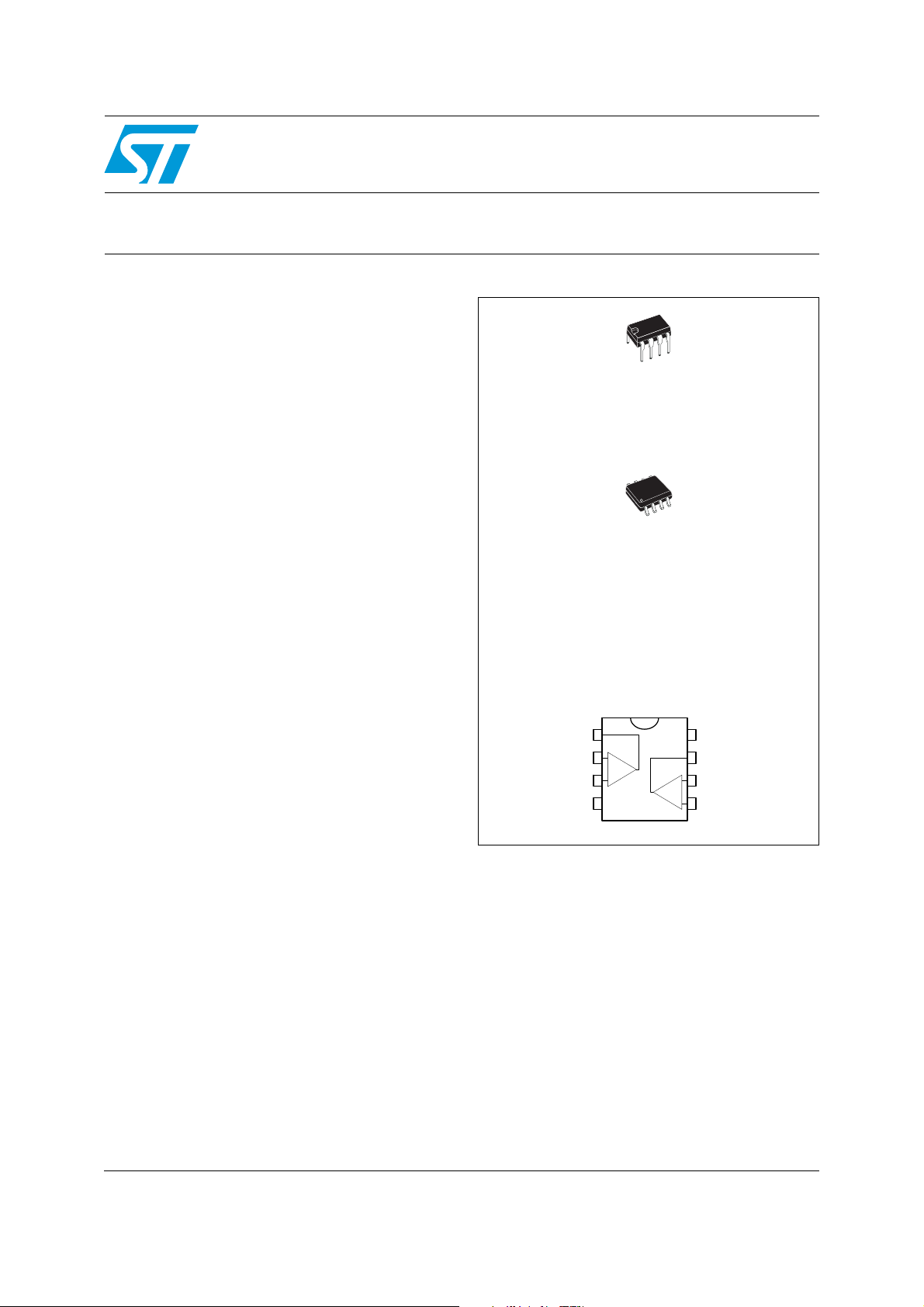
LM833
Low noise dual operational amplifier
N
DIP8
(Plastic package)
■ Audio systems
■ Preamplification, filtering
Description
The LM833 is a monolithic dual operational
amplifier particularly well-suited to audio
applications.
It offers low voltage noise (4.5 nV/√Hz) and high
frequency performances (15 MHz gain bandwidth
product, 7 V/µs slew rate).
In addition, the LM833 has a very low distortion
(0.002%) and excellent phase/gain margins.
Inverting input 1
Non-inverting input 1
D
SO-8
(Plastic micropackage)
Pin connections (top view)
-
+
V
8
CC
Output 2
7
6
Inverting input 2
Non-inverting input 2
1
Output 1
2
-
+
3
45
-
V
CC
+
August 2009 Doc ID 2169 Rev 3 1/12
www.st.com
12
Absolute maximum ratings LM833
1 Absolute maximum ratings
Table 1. Key parameters and their absolute maximum ratings
Symbol Parameter Value Unit
V
CC
V
id
V
Supply voltage ±18 or +36 V
Differential input voltage
Input voltage
i
Input current
(1)
(1)
(2)
: Vin driven negative
5 mA in DC or 50 mA in
±30 V
±15 V
AC (duty cycle = 10%,
I
in
Input current
(3)
: Vin driven positive above
AMR value
T=1s)
0.4
mA
Output short-circuit duration Infinite s
T
T
stg
Ptot
ESD
1. Either or both input voltages must not exceed the magnitude of Vcc+ or Vcc-.
2. This input current only exists when the voltage at any of the input leads is driven negative. It is due to the
collector-base junction of the input PNP transistor becoming forward-biased and thereby acting as input
diode clamp. In addition to this diode action, there is NPN parasitic action on the IC chip. This transistor
action can cause the output voltages of the Op-amps to go to the V
overdrive) for the time during which an input is driven negative.
This is not destructive and normal output is restored for input voltages above -0.3 V.
3. The junction base/substrate of the input PNP transistor polarized in reverse must be protected by a resistor
in series with the inputs to limit the input current to 400 µA max (R = (Vin - 36 V)/400 µA).
4. Power dissipation must be considered to ensure maximum junction temperature (Tj) is not exceeded.
5. Human body model: 100 pF discharged through a 1.5 kΩ resistor between two pins of the device, done for
all couples of pin combinations with other pins floating.
6. Machine model: a 200 pF capacitor is charged to the specified voltage, then discharged directly between
two pins of the device with no external series resistor (internal resistor < 5 Ω), done for all couples of pin
combinations with other pins floating.
7. Charged device model: all pins plus package are charged together to the specified voltage and then
discharged directly to the ground.
Junction temperature +150 °C
j
Storage temperature -65 to +150 °C
Maximum power dissipation
HBM: human body model
MM: machine model
(5)
(6)
CDM: charged device model
(4)
(7)
CC
500 mW
2kV
200 V
1.5 kV
voltage level (or to ground for a large
Table 2. Operating conditions
Symbol Parameter Value Unit
T
V
CC
oper
Supply voltage ±2.5 to ±15 V
Operating free-air temperature range -40 to 105 °C
2/12 Doc ID 2169 Rev 3
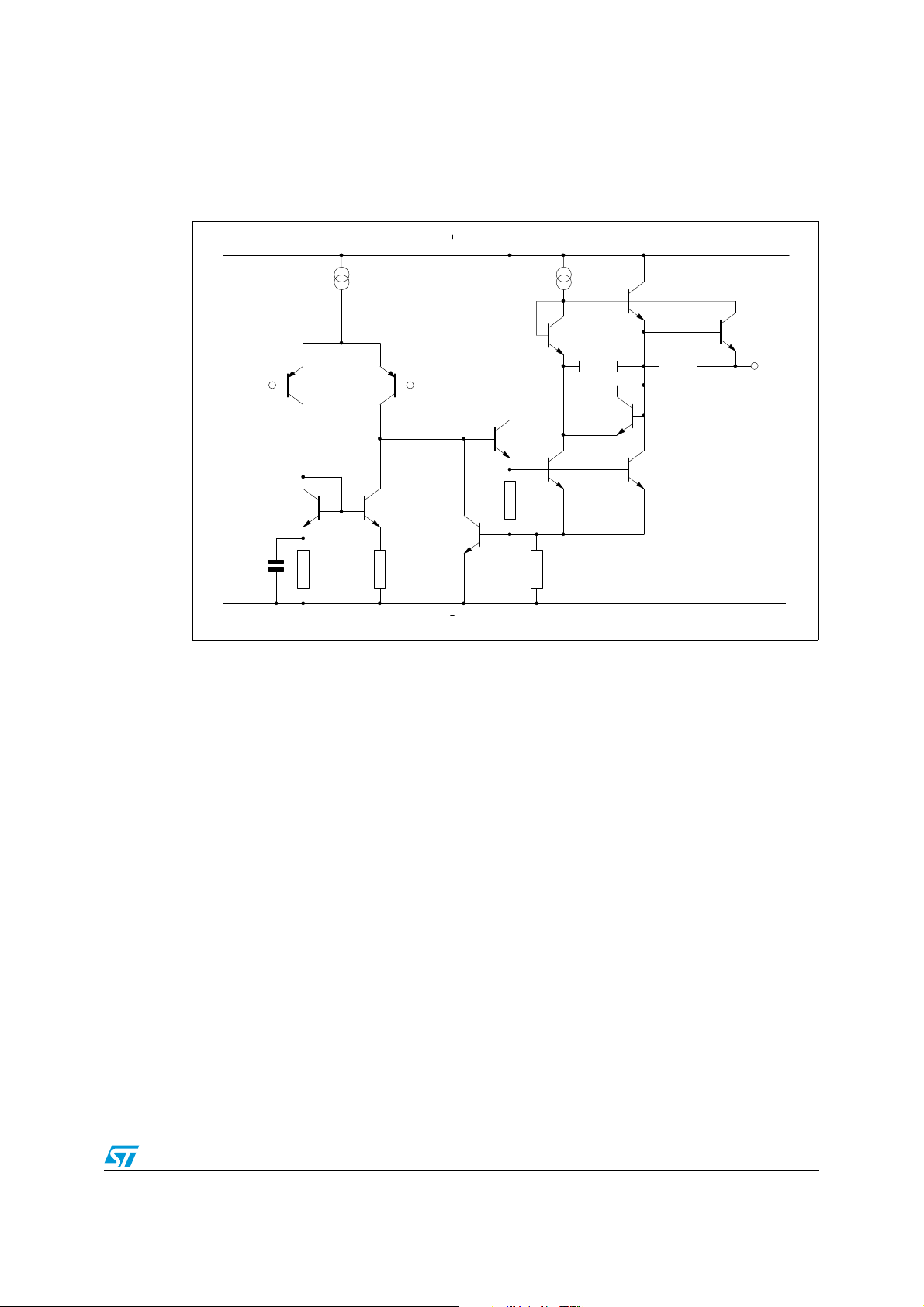
LM833 Typical application schematics
2 Typical application schematics
Figure 1. Schematic diagram (1/2 LM833)
V
CC
Inverting
Input
Non-inverting
Input
V
CC
Output
Doc ID 2169 Rev 3 3/12
Electrical characteristics LM833
3 Electrical characteristics
Table 3. V
Symbol Parameter Min. Typ. Max. Unit
= +15 V, V
CC+
= -15 V, T
CC-
= 25° C (unless otherwise specified)
amb
V
DV
V
A
Input offset voltage (Rs = 10 Ω, Vo = 0 V, Vic = 0 V)
io
Input offset voltage drift
I
io
I
ib
icm
io
vd
= 10 Ω, Vo = 0 V, T
R
s
min.
≤ T
amb
≤ T
max.
Input offset current (Vo = 0 V, Vic = 0 V)
Input bias current (Vo = 0 V, Vic = 0 V)
Input common mode voltage range ±12 ±14 V
Large signal voltage gain (RL = 2 kΩ, Vo = ±10 V)
0.3 5 mV
2
25 200 nA
300 1000 nA
90 100 dB
Output voltage swing (Vid = ±1 V)
±V
CMR
SVR
I
CC
SR
GBP
= 2.0 kΩ
R
opp
L
RL = 2.0 kΩ
= 10 kΩ
R
L
RL = 10 kΩ
Common-mode rejection ratio (V
Supply voltage rejection ratio
(V
CC+/VCC-
= +15 V/-15 V to +5 V/-5 V)
Supply current (Vo = 0 V, all amplifiers)
Slew rate (V
= -10 V to +10 V, RL = 2 kΩ, AV = +1)
i
Gain bandwidth product
(R
= 2 kΩ, CL = 100 pF, f = 100 kHz)
L
= ±13 V)
ic
101213.7
-14
-10
13.9
-14.4
-12
80 100 dB
80 105 dB
48 mA
57 V/µs
10 15 MHz
B Unity gain bandwidth (open loop) 9 MHz
µV/°C
V
φm
e
i
THD
V
O1/VO2
FPB
Phase margin (R
Equivalent input noise voltage (RS = 100 Ω, f = 1 kHz)
n
Equivalent input noise current (f = 1 kHz) 0.5
n
Total harmonic distortion
= 2 kΩ, f = 20 Hz to 20 kHz, Vo = 3 V
(R
L
Channel separation (f = 20 Hz to 20 kHz) 120 dB
Full power bandwidth (Vo = 27 Vpp, RL = 2 kΩ, THD ≤ 1%)
= 2 kΩ)
L
4/12 Doc ID 2169 Rev 3
, AV = +1)
rms
60 Degrees
nV
4.5
------------
pA
------------
0.002 %
120 kHz
Hz
Hz

LM833 Electrical characteristics
)
Figure 2. Total supply current vs. supply
voltage
5
4.5
4
3.5
3
2.5
2
1.5
Total Supply Current (mA)
1
0.5
0
0 5 10 15 20 25 30
Supply Voltage (V)
Figure 4. Equivalent input noise voltage vs.
frequency
VCC = ±15V, G = 100
= 100, T
R
s
amb
= 25°C
Figure 3. Output voltage vs. supply voltage
15
10
5
Vid = ±1V
= 600Ω
0
-5
Output Voltage (V)
-10
-15
0 5 10 15
Supply Voltage (V)
R
L
Figure 5. Output short circuit current vs.
output voltage
50
40
30
20
10
0
-10
-20
Output Short Circuit Current (mA
-30
-40
0102030
VCC = 0/30V
T
amb
Output V oltage (V )
= 25°C
Figure 6. Output voltage vs. supply voltage Figure 7. THD+ noise vs. frequency
15
10
5
0
-5
Output Voltage (V)
-10
-15
0 5 10 15
Supply Voltage (V)
Vid = ±1V
= 2kΩ
R
L
Doc ID 2169 Rev 3 5/12
1
0.1
0.01
THD+Noise (%)
0.001
0.01 0.1 1 10 100
RL = 2kΩ, Vo = 3V
VCC = ±15V, Av = 1
Frequency (kHz)
rms

Electrical characteristics LM833
Figure 8. Voltage gain and phase vs.
frequency
50
40
30
gain
20
10
Gain (dB)
0
-10
RL = 2kΩ, CL = 100pF
= ±15V, G = -100
V
-20
CC
-30
10 100 1000 10000 100000
Frequency (kHz)
phase
Figure 9. THD + noise vs. Vout
180
120
60
0
-60
-120
Phase (Deg)
1.000
0.100
0.010
THD+Noise (%)
0.001
12345678910
RL = 2kΩ, f = 1kHz
V
= ±15V, Av = 10
CC
Vout (Vrms)
6/12 Doc ID 2169 Rev 3

LM833 Package information
4 Package information
In order to meet environmental requirements, ST offers these devices in different grades of
ECOPACK
specifications, grade definitions and product status are available at: www.st.com.
ECOPACK
®
packages, depending on their level of environmental compliance. ECOPACK®
®
is an ST trademark.
Doc ID 2169 Rev 3 7/12

Package information LM833
4.1 DIP8 package information
Figure 10. DIP8 package mechanical drawing
Table 4. DIP8 package mechanical data
Dimensions
Ref.
Min. Typ. Max. Min. Typ. Max.
A5.330.210
A1 0.38 0.015
A2 2.92 3.30 4.95 0.115 0.130 0.195
b 0.36 0.46 0.56 0.014 0.018 0.022
b2 1.14 1.52 1.78 0.045 0.060 0.070
c 0.20 0.25 0.36 0.008 0.010 0.014
D 9.02 9.27 10.16 0.355 0.365 0.400
E 7.62 7.87 8.26 0.300 0.310 0.325
E1 6.10 6.35 7.11 0.240 0.250 0.280
e 2.54 0.100
eA 7.62 0.300
eB 10.92 0.430
L 2.92 3.30 3.81 0.115 0.130 0.150
Millimeters Inches
8/12 Doc ID 2169 Rev 3

LM833 Package information
4.2 SO-8 package information
Figure 11. SO-8 package mechanical drawing
Table 5. SO-8 package mechanical data
Dimensions
Ref.
Min. Typ. Max. Min. Typ. Max.
A1.750.069
A1 0.10 0.25 0.004 0.010
A2 1.25 0.049
b 0.28 0.48 0.011 0.019
c 0.17 0.23 0.007 0.010
D 4.80 4.90 5.00 0.189 0.193 0.197
E 5.80 6.00 6.20 0.228 0.236 0.244
E1 3.80 3.90 4.00 0.150 0.154 0.157
e 1.27 0.050
h 0.25 0.50 0.010 0.020
L 0.40 1.27 0.016 0.050
L1 1.04 0.040
k 0 8° 1° 8°
Millimeters Inches
ccc 0.10 0.004
Doc ID 2169 Rev 3 9/12

Ordering information LM833
5 Ordering information
Table 6. Order codes
Part number
LM833N
LM833D/DT SO-8 Tube or tape & reel 833
Temperature
range
-40, +105° C
Package Packing Marking
DIP8 Tube LM833N
10/12 Doc ID 2169 Rev 3

LM833 Revision History
6 Revision History
Table 7. Document revision history
Date Revision Changes
01-Nov-2001 1 Initial release.
01-Jul-2005 2
20-Aug-2009 3
PPAP references inserted in the datasheet seeTable on page 1.
ESD protection inserted in Table 1 on page 2.
Document reformatted.
Minor text changes.
Updated packages in Chapter 4: Package information.
Removed automotive grade versions (LM833YD/DT) from
Chapter 5: Ordering information
Doc ID 2169 Rev 3 11/12

LM833
Please Read Carefully:
Information in this document is provided solely in connection with ST products. STMicroelectronics NV and its subsidiaries (“ST”) reserve the
right to make changes, corrections, modifications or improvements, to this document, and the products and services described herein at any
time, without notice.
All ST products are sold pursuant to ST’s terms and conditions of sale.
Purchasers are solely responsible for the choice, selection and use of the ST products and services described herein, and ST assumes no
liability whatsoever relating to the choice, selection or use of the ST products and services described herein.
No license, express or implied, by estoppel or otherwise, to any intellectual property rights is granted under this document. If any part of this
document refers to any third party products or services it shall not be deemed a license grant by ST for the use of such third party products
or services, or any intellectual property contained therein or considered as a warranty covering the use in any manner whatsoever of such
third party products or services or any intellectual property contained therein.
UNLESS OTHERWISE SET FORTH IN ST’S TERMS AND CONDITIONS OF SALE ST DISCLAIMS ANY EXPRESS OR IMPLIED
WARRANTY WITH RESPECT TO THE USE AND/OR SALE OF ST PRODUCTS INCLUDING WITHOUT LIMITATION IMPLIED
WARRANTIES OF MERCHANTABILITY, FITNESS FOR A PARTICULAR PURPOSE (AND THEIR EQUIVALENTS UNDER THE LAWS
OF ANY JURISDICTION), OR INFRINGEMENT OF ANY PATENT, COPYRIGHT OR OTHER INTELLECTUAL PROPERTY RIGHT.
UNLESS EXPRESSLY APPROVED IN WRITING BY AN AUTHORIZED ST REPRESENTATIVE, ST PRODUCTS ARE NOT
RECOMMENDED, AUTHORIZED OR WARRANTED FOR USE IN MILITARY, AIR CRAFT, SPACE, LIFE SAVING, OR LIFE SUSTAINING
APPLICATIONS, NOR IN PRODUCTS OR SYSTEMS WHERE FAILURE OR MALFUNCTION MAY RESULT IN PERSONAL INJURY,
DEATH, OR SEVERE PROPERTY OR ENVIRONMENTAL DAMAGE. ST PRODUCTS WHICH ARE NOT SPECIFIED AS "AUTOMOTIVE
GRADE" MAY ONLY BE USED IN AUTOMOTIVE APPLICATIONS AT USER’S OWN RISK.
Resale of ST products with provisions different from the statements and/or technical features set forth in this document shall immediately void
any warranty granted by ST for the ST product or service described herein and shall not create or extend in any manner whatsoever, any
liability of ST.
ST and the ST logo are trademarks or registered trademarks of ST in various countries.
Information in this document supersedes and replaces all information previously supplied.
The ST logo is a registered trademark of STMicroelectronics. All other names are the property of their respective owners.
© 2009 STMicroelectronics - All rights reserved
STMicroelectronics group of companies
Australia - Belgium - Brazil - Canada - China - Czech Republic - Finland - France - Germany - Hong Kong - India - Israel - Italy - Japan -
Malaysia - Malta - Morocco - Philippines - Singapore - Spain - Sweden - Switzerland - United Kingdom - United States of America
www.st.com
12/12 Doc ID 2169 Rev 3
 Loading...