How it Works
Log In / Sign Up
Buy Points
How it Works
FAQ
Contact Us
Questions and Suggestions
Users
Datasheet
Loading...
L
LM2903QDR
LM2903QP
LM2903V
3
LM2903VD
LM2903VDR2
LM2903VN
LM2903W
LM2903WDT
LM2903YPT
LM2904
9
LM2904A
2
LM2904ADMG
LM2904ADMR2G
LM2904ANG
LM2904AVQDR
LM2904AVQPWR
LM2904D
5
LM2904DG
LM2904DGKR
LM2904DMR2G
LM2904DP
LM2904DR
LM2904DR2
LM2904DR2G
LM2904D-ST
LM2904M
2
LM2904MWC
LM2904MX
2
LM2904N
7
LM2904NG
LM2904P
2
LM2904PS
LM2904PSR
LM2904PW
LM2904PWLE
LM2904PWR
LM2904-Q1
LM2904QD
LM2904QDR
2
LM2904QP
LM2904V
2
LM2904VD
LM2904VDG
LM2904VDMR2G
LM2904VDR2
LM2904VDR2G
LM2904VN
LM2904VNG
LM2904VQDR
LM2904VQPWR
LM2904W
LM2904WH
LM2907M-8
LM2907MX-8
LM2907N
LM2907N-8
LM2907N-NOPB
LM2917M
LM2917M-8
LM2917MX
LM2917MX-8
LM2917N
LM2917N-8
LM2924N
LM2925T
LM2926T
2
LM2927S
LM2927T
2
LM293
7
LM2930-5.0MDC
LM2930-5.0MWC
LM2930-8.0MWC
LM2930S-5.0
LM2930S-8.0
LM2930SX-5.0
LM2930SX-8.0
LM2930T-8.0
LM2931
4
LM2931A
LM2931ACD
LM2931ACD2T
LM2931ACD2TR4
LM2931ACDR2
LM2931ACT
LM2931ACT-5.0
LM2931ACTH
LM2931ACTV
LM2931AD
LM2931AD2T
LM2931AD2T-5.0
LM2931AD2T-5.0R4
LM2931AD33
LM2931AD-5.0
2
LM2931AD-5.0R2
LM2931ADT
LM2931ADT-1-5.0
LM2931ADT33
LM2931ADT50
2
LM2931ADT-5.0RK
LM2931AM-5.0
2
Loading...
Loading...
Nothing found
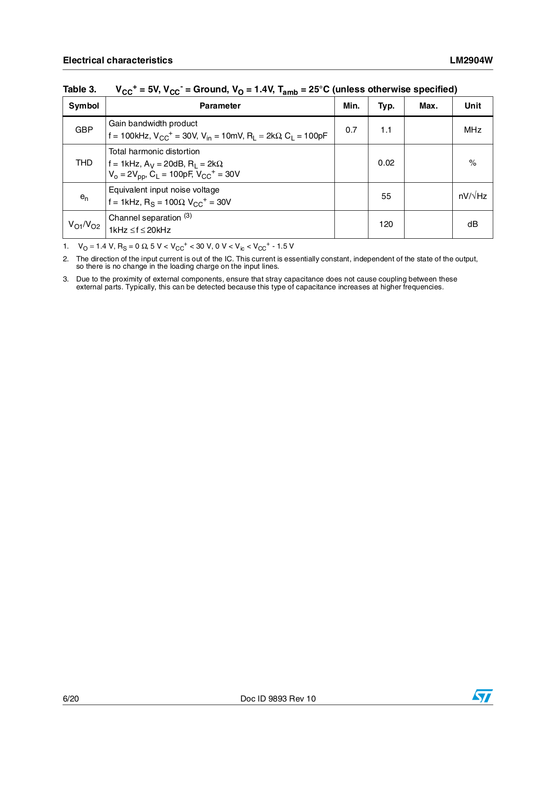
LM2904W
Datasheet (ST)
20 pgs
432.87 Kb
0
Table of contents
Loading...
Datasheet LM2904W Datasheet (ST)
...
Datasheet Datasheet (ST)
Download
Specifications and Main Features
Frequently Asked Questions
User Manual
Download
Loading...
+
hidden pages
Unhide
You need points to download manuals.
1 point = 1 manual.
You can buy points or you can get point for every manual you upload.
Buy points
Upload your manuals
 Loading...

")