

ST LM124, LM224, LM324 Operation Manual
Low power quad operational amplifiers
Features
■ Wide gain bandwidth: 1.3 MHz
■ Input common-mode voltage range includes
ground
■ Large voltage gain: 100 dB
■ Very low supply current per amplifier: 375 µA
■ Low input bias current: 20 nA
■ Low input offset voltage: 5 mV max.
■ Low input offset current: 2 nA
■ Wide power supply range:
– Single supply: +3 V to +30 V
■ Dual supplies: ±1.5 V to ±15 V
Description
LM124, LM224, LM324
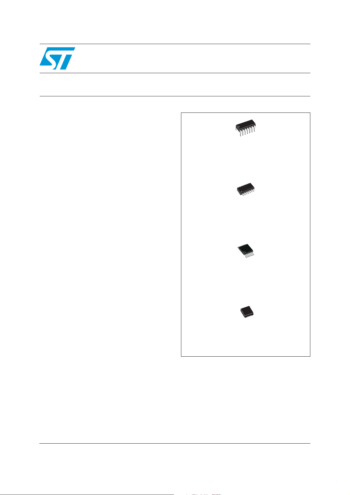
N
DIP14
(Plastic package)
D
SO-14
(Plastic micropackage)
The LM124, LM224 and LM324 consist of four
independent, high gain, internally frequencycompensated operational amplifiers. They
operate from a single power supply over a wide
range of voltages. Operation from split power
supplies is also possible and the low power
supply current drain is independent of the
magnitude of the power supply voltage.
P
TSSOP-14
(Thin shrink small outline package)
Q
QFN16 3x3
(Plastic micropackage)
June 2011 Doc ID 2156 Rev 7 1/19
www.st.com
19
Pin and schematic diagram LM124, LM224, LM324
1 Pin and schematic diagram
Figure 1. Pin connections (top view)
Output 1
Inverting Input 1
Non-inverting Input 1
V
CC
Non-inverting Input 2
Inverting Input 2
Output 2
IN1+
IN1+
VCC+
VCC+
IN2+
NC
NC
1
2
-
+
3
+
4
5
+
-
6
-
+
+
-
7
OUT1
OUT4
OUT1
IN1-
IN1-
16
16
1
1
2
2
3
3
4
5
IN2-
OUT4
14
15
14
15
6
7
OUT3
OUT2
14
13
12
11
10
9
8
IN4-
IN4-
13
13
12
12
11
11
10
10
9
8
IN3-
Output 4
Inverting Input 4
Non-inverting Input 4
-
V
CC
Non-inverting Input 3
Inverting Input 3
Output 3
IN4+
IN4+
VCC-
VCC-
NC
NC
IN3+
Figure 2. Schematic diagram (1/4 LM124)
2/19 Doc ID 2156 Rev 7
LM124, LM224, LM324 Absolute maximum ratings
2 Absolute maximum ratings
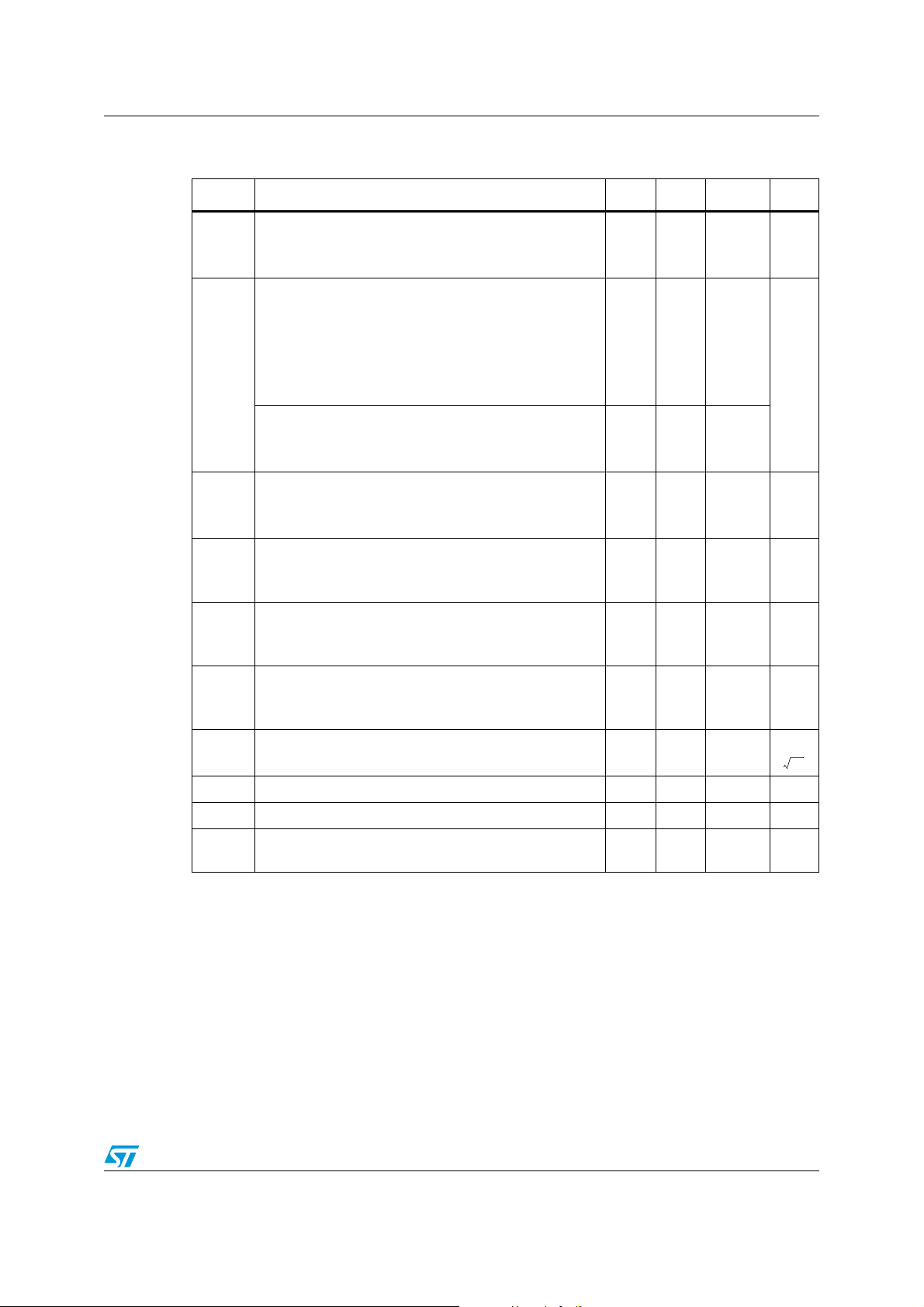
Table 1. Absolute maximum ratings
Symbol Parameter LM124 LM224 LM324 Unit
V
T
T
R
Supply voltage ±16 or 32 V
CC
V
Input voltage
in
Differential input voltage
V
id
Output short-circuit duration
Input current
I
Input current
in
AMR value
Operating free-air temperature range -55 to +125 -40 to +105 0 to +70 °C
oper
Storage temperature range -65 to +150 °C
stg
T
Maximum junction temperature 150 °C
j
Thermal resistance junction to ambient
SO14
TSSOP14
thja
DIP14
QFN16 3x3
(1)
(2)
(3)
(4)
: Vin driven negative
(5)
: Vin driven positive above
-0.3 to 32 V
32 V
Infinite
5 mA in DC or 50 mA in AC (duty cycle = 10%, T=1s)
0.4
(6)
103
100
83
45
mA
°C/W
Thermal resistance junction to case
SO14
R
thjc
TSSOP14
DIP14
QFN16
HBM: human body model
ESD
CDM: charged device model
1. Either or both input voltages must not exceed the magnitude of V
are with respect to ground terminal.
2. Differential voltages are the non-inverting input terminal with respect to the inverting input terminal.
3. Short-circuits from the output to V
approximately 40 mA independent of the magnitude of V
circuits on all amplifiers.
4. This input current only exists when the voltage at any of the input leads is driven negative. It is due to the collector-base
junction of the input PNP transistor becoming forward-biased and thereby acting as input diode clamp. In addition to this
diode action, there is NPN parasitic action on the IC chip. This transistor action can cause the output voltages of the opamps to go to the V
This is not destructive and normal output is restored for input voltages above -0.3 V.
5. The junction base/substrate of the input PNP transistor polarized in reverse must be protected by a resistor in series with
the inputs to limit the input current to 400 µA max (R = (Vin - 32 V)/400 µA).
6. Short-circuits can cause excessive heating. Destructive dissipation can result from simultaneous short-circuits on all
amplifiers. These are typical values given for a single layer board (except for TSSOP, a two-layer board).
7. Human body model, 100 pF discharged through a 1.5 kΩ resistor into pin of device.
8. Machine model ESD: a 200 pF capacitor is charged to the specified voltage, then discharged directly into the IC with no
external series resistor (internal resistor < 5 Ω), into pin-to-pin of device.
9. Charged device model: all pins plus package are charged together to the specified voltage and then discharged directly to
ground.
voltage level (or to ground for a large overdrive) for the time during which an input is driven negative.
CC
(7)
(8)
(9)
+
-
or V
CC
can cause excessive heating if VCC > 15 V. The maximum output current is
CC
. Destructive dissipation can result from simultaneous short-
CC
. All voltage values, except differential voltages
CC
31
32
33
14
250
150
1500
°C/W
VMM: machine model
Doc ID 2156 Rev 7 3/19
Electrical characteristics LM124, LM224, LM324
3 Electrical characteristics
Table 2. V
+
= +5 V, V
CC
-
= ground, Vo = 1.4 V, T
CC
= +25° C (unless otherwise
amb
specified)
Symbol Parameter Min. Typ. Max. Unit
≤ T
≤ T
≤ T
≤ T
(3)
≤ T
≤ T
max
max
max
(2)
max
max
max
max
max
(1)
≤ 10 kΩ)
s
≤ 10 kΩ)
s
25
230
20 150
5025100
6565110
0.7
1.5
0.8
1.5
0
0
70
80 dB
60
7
7
9
100
300
1.2
3
1.2
3
VCC -1.5
-2
V
CC
V/mV
V
I
io
I
ib
A
vd
SVR
I
CC
V
icm
CMR
I
source
Input offset voltage
T
= +25° C
amb
LM124-LM224
io
LM324
T
min
≤ T
amb
≤ T
LM124-LM224
LM324
Input offset current
T
= +25° C
amb
T
≤ T
min
amb
Input bias current
T
= +25° C
amb
T
≤ T
min
amb
Large signal voltage gain
+
= +15 V, RL = 2 kΩ, Vo = 1.4 V to 11.4 V
V
CC
= +25° C
T
amb
T
≤ T
min
amb
Supply voltage rejection ratio (R
+
V
= 5 V to 30 V
CC
= +25° C
T
amb
T
≤ T
min
amb
Supply current, all Amp, no load
= +25° C
T
amb
VCC = +5 V
V
= +30 V
CC
≤ T
T
min
amb
≤ T
VCC = +5 V
V
= +30 V
CC
Input common mode voltage range
= +30 V
V
CC
T
= +25° C
amb
T
≤ T
min
amb
Common mode rejection ratio (R
T
= +25° C
amb
T
≤ T
min
amb
Output current source (Vid = +1 V)
= +15 V, Vo = +2 V 20 40 70 mA
V
CC
mV
nA
nA
dB
mA
V
4/19 Doc ID 2156 Rev 7
LM124, LM224, LM324 Electrical characteristics
Table 2. V
+
= +5 V, V
CC
-
= ground, Vo = 1.4 V, T
CC
= +25° C (unless otherwise
amb
specified) (continued)
Symbol Parameter Min. Typ. Max. Unit
Output sink current (Vid = -1 V)
I
sink
V
V
SR
VCC = +15 V, Vo = +2 V
V
= +15 V, Vo = +0.2 V
CC
High level output voltage
= +30 V
V
CC
T
= +25° C, RL = 2 kΩ
amb
T
≤ T
≤ T
amb
max
= +25° C, RL = 10 kΩ
≤ T
≤ T
amb
max
= +25°C
≤ T
≤ T
amb
max
OH
min
T
amb
T
min
= +5 V, RL = 2 kΩ
V
CC
T
amb
T
min
Low level output voltage (RL = 10 kΩ)
= +25°C
OL
T
T
amb
min
≤ T
amb
≤ T
max
Slew rate
= 15 V, Vi = 0.5 to 3 V, RL = 2 kΩ, CL = 100 pF,
V
CC
unity gain
10
12
26
26
27
27
3.5
20
50
27
28
3
52020mV
0.4 V/µs
mA
µA
V
Gain bandwidth product
GBP
= 30 V, f = 100 kHz, V
V
CC
= 100 pF
C
L
= 10 mV, RL = 2 kΩ,
in
1.3 MHz
Total harmonic distortion
THD
f = 1 kHz, A
= 20 dB, RL = 2 kΩ, Vo = 2 Vpp,
v
0.015 %
CL = 100 pF, VCC = 30 V
Equivalent input noise voltage
e
n
f = 1 kHz, R
DV
DI
V
o1/Vo2
1. Vo = 1.4 V, Rs = 0 Ω, 5 V < V
2. The direction of the input current is out of the IC. This current is essentially constant, independent of the
3. The input common-mode voltage of either input signal voltage should not be allowed to go negative by
4. Due to the proximity of the external components, ensure that stray capacitance between these external
Input offset voltage drift 7 30 µV/°C
io
Input offset current drift 10 200 pA/°C
io
Channel separation
1 kHz ≤ f ≤ 20 kHZ
state of the output so there is no change in the load on the input lines.
more than 0. V. The upper end of the common-mode voltage range is V
can go to +32 V without damage.
parts does not cause coupling. Coupling can be detected because this type of capacitance increases at
higher frequencies.
= 100 Ω, VCC = 30 V
s
(4)
+
< 30 V, 0 < Vic < V
CC
CC
+
- 1.5 V.
+
- 1.5 V, but either or both inputs
CC
40
120 dB
nV
-----------Hz
Doc ID 2156 Rev 7 5/19
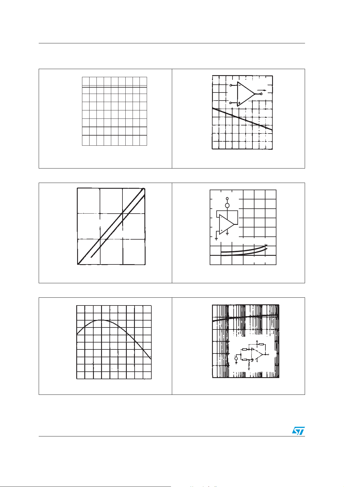
Electrical characteristics LM124, LM224, LM324
Figure 3. Input bias current vs. ambient
Figure 4. Current limiting
temperature
IB (nA)
24
21
18
15
12
9
6
3
0
-55-35-15 5
25
Ambient temperature (°C)
45
6585105 125
90
80
70
60
50
40
30
Input current (mA)
20
10
0
-55
-15
-35
5
Temperature (°C)
25
Figure 5. Input voltage range Figure 6. Supply current
15
10
5
Input voltage (V)
Negative
Positive
4
3
2
1
Supply current (mA)
mA
V
CC
I
D
Tamb = 0°C to +125°C
IO+
45 65 85105
125
Tamb = -55°C
051015
Powe r supply voltage (V)
0
10
20 30
Positive supply voltage (V)
Figure 7. Gain bandwidth product Figure 8. Common mode rejection ratio
GBP (MHz)
1.35
1.30
1.25
1.2
1.15
1.1
1.05
0.95
Gain bandwidth product (MHz)
0.9
1
-55
-15
-35
5
Ambient temperature (°C)
45 65 85105
25
125
120
100
80
60
40
20
Common-mode rejection ratio (dB)
0
100
+7.5 V
100 Ω
100 Ω
e
I
100 kΩ
10k 100k
1k
Frequency (Hz)
100 kΩ
+7.5 V
e
O
1M
6/19 Doc ID 2156 Rev 7
 Loading...