

Low current 1.2 to 37V adjustable voltage regulator
Features
■ Output voltage range: 1.2 to 37V
■ Output current in excess of 100 mA
■ Line regulation typ. 0.01%
■ Load regulation typ. 0.1%
■ Thermal overload protection
■ Short circuit protection
■ Output transition safe area compensation
■ Floating operation for high voltage applications
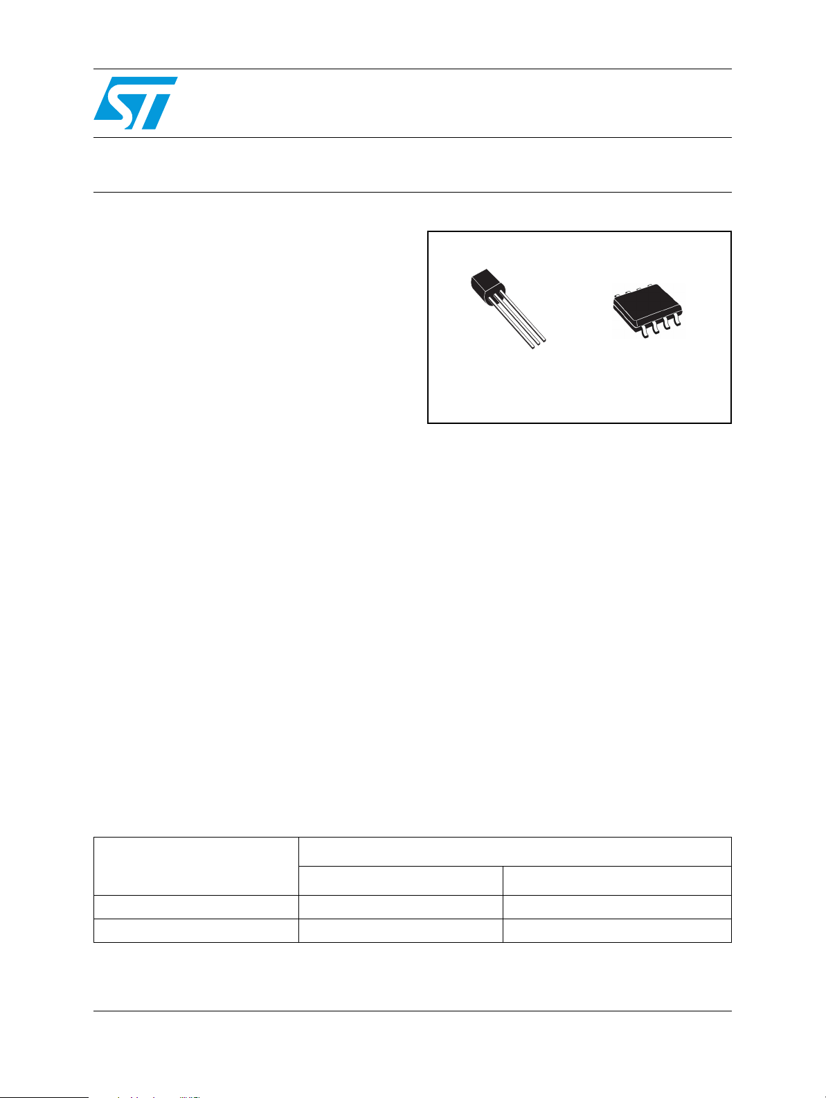
TO-92
LM217L
LM317L
SO-8
Description
The LM217L/LM317L are monolithic integrated
circuit in SO-8 and TO-92 packages intended for
use as positive adjustable voltage regulators.
They are designed to supply until 100 mA of load
current with an output voltage adjustable over a
1.2 to 37V range.
Order codes
Part numbers
SO-8 (Tape & reel) TO-92 (BAG)
The nominal output voltage is selected by means
of only a resistive divider, making the device
exceptionally easy to use and eliminating the
stocking of many fixed regulators.
Packages
(1)
LM217L LM217LD13TR LM217LZ
LM317L LM317LD13TR LM317LZ
1. Available in tape & reel with the suffix "-TR" and in Ammopak with the suffix "-AP". Please note that in these cases pins are
shaped according to tape & reel specifications
May 2007 Rev. 4 1/18
www.st.com
18

LM217L/LM317L
Contents
1 Diagram . . . . . . . . . . . . . . . . . . . . . . . . . . . . . . . . . . . . . . . . . . . . . . . . . . . 3
2 Pin configuration . . . . . . . . . . . . . . . . . . . . . . . . . . . . . . . . . . . . . . . . . . . 4
3 Maximum ratings . . . . . . . . . . . . . . . . . . . . . . . . . . . . . . . . . . . . . . . . . . . . 5
4 Electrical characteristics . . . . . . . . . . . . . . . . . . . . . . . . . . . . . . . . . . . . . 6
5 Typical performance . . . . . . . . . . . . . . . . . . . . . . . . . . . . . . . . . . . . . . . . . 8
6 Application information . . . . . . . . . . . . . . . . . . . . . . . . . . . . . . . . . . . . . . 9
7 Application circuits . . . . . . . . . . . . . . . . . . . . . . . . . . . . . . . . . . . . . . . . . 10
8 Package mechanical data . . . . . . . . . . . . . . . . . . . . . . . . . . . . . . . . . . . . 12
9 Revision history . . . . . . . . . . . . . . . . . . . . . . . . . . . . . . . . . . . . . . . . . . . 17
2/18
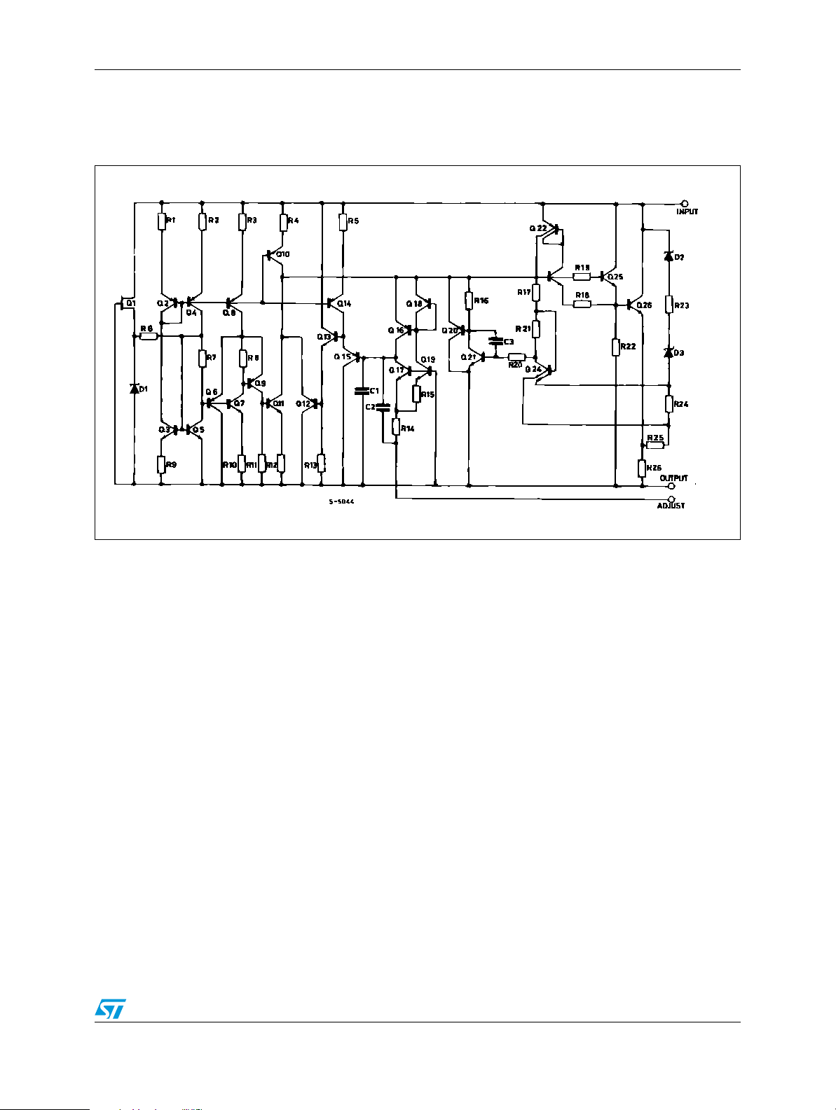
LM217L/LM317L Diagram
1 Diagram
Figure 1. Schematic diagram
3/18
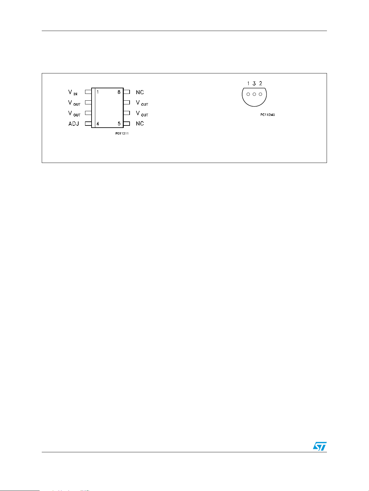
Pin configuration LM217L/LM317L
2 Pin configuration
Figure 2. Pin connections (top view for SO-8, bottom view for TO-92)
PIN 1 = ADJUST
PIN 2 = IN
PIN 3 = OUT
SO-8
TO-92
4/18
LM217L/LM317L Maximum ratings
3 Maximum ratings
Table 1. Absolute maximum ratings
Symbol Parameter Value Unit
V
T
T
I-VO
P
OP
STG
Input-output differential voltage 40 V
Power dissipation Internally Limited mW
D
Operating junction temperature range
Storage temperature range -55 to 150 °C
Figure 3. Test circuit
for LM217L -40 to 125
°C
for LM317L 0 to 125
5/18
Electrical characteristics LM217L/LM317L
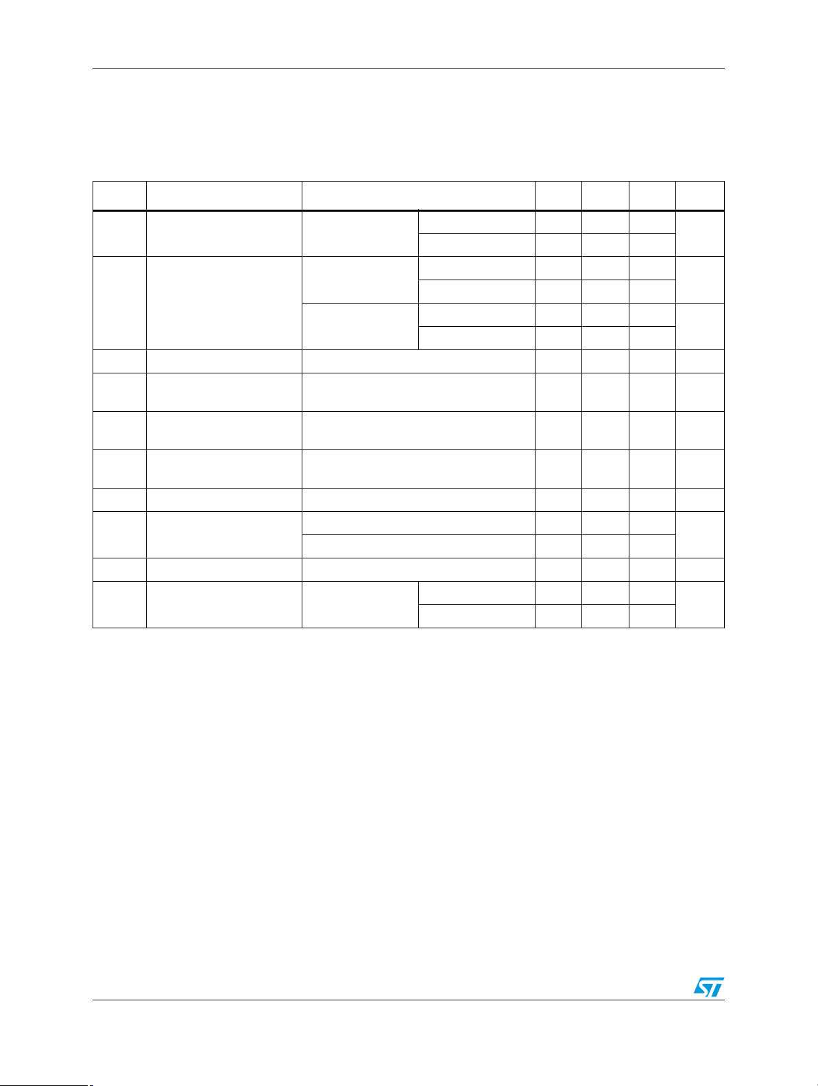
4 Electrical characteristics
Table 2. Electrical characteristics of LM217L (refer to the test circuits, TJ = - 40 to 125°C,
V
- VO = 5 V, IO = 40 mA, unless otherwise specified)
I
Symbol Parameter Test conditions Min. Typ. Max. Unit
= 25°C 0.01 0.02
T
J
0.02 0.05
= 25°C 5 15
T
J
20 50
= 25°C 0.1 0.3
T
J
0.3 1
0.2 5 µA
1.2 1.25 1.3 V
%/V
mV
%
ΔI
V
ΔV
ΔV
I
ADJ
- VO = 3 to 40 V
V
Line regulation
O
I
< 20 mA
I
L
VO ≤ 5 V
IO = 5 to 100 mA
Load regulation
O
≥ 5 V
V
O
= 5 to 100 mA
I
O
Adjustment pin current 50 100 µA
- VO = 3 to 40 V, IO = 5 to 100 mA
V
Adjustment pin current
ADJ
Reference voltage
REF
I
< 625 mW
P
d
- VO = 3 to 40 V, IO = 10 to 500 mA
V
I
Pd < 625 mW
ΔVO/V
I
O(min)
Output voltage
O
temperature stability
Minimum load current VI - VO = 40 V 3.5 5 mA
VI - VO = 3 to 13 V 100 200
I
O(max)
Maximum output current
- VO = 40 V 50
V
I
eN Output noise voltage B = 10 Hz to 10 KHz, T
TJ = 25°C
SVR Supply voltage rejection
1. C
is connected between adjust pin and ground.
ADJ
(1)
f = 120 Hz
0.7 %
= 25°C 0.003 %
J
= 0 65
C
ADJ
= 10 µF 66 80
C
ADJ
mA
dB
6/18

LM217L/LM317L Electrical characteristics
Table 3. Electrical characteristics of LM317L (refer to the test circuits, TJ = 0 to 125°C,
V
- VO = 5 V, IO = 40 mA, unless otherwise specified)
I
Symbol Parameter Test conditions Min. Typ. Max. Unit
= 25°C 0.01 0.04
T
ΔVOLine regulation
ΔV
I
ΔI
V
Load regulation
O
Adjustment pin current 50 100 µA
ADJ
Adjustment pin current
ADJ
Reference voltage
REF
- VO = 3 to 40 V
V
I
< 20 mA
I
L
VO ≤ 5 V
IO = 5 to 100 mA
≥ 5 V
V
O
= 5 to 100 mA
I
O
- VO = 3 to 40 V, IO = 5 to 100 mA
V
I
< 625 mW
P
d
- VO = 3 to 40 V, IO = 5 to 100 mA
V
I
Pd < 625 mW
J
0.02 0.07
= 25°C 5 25
T
J
20 70
= 25°C 0.1 0.5
T
J
0.3 1.5
0.2 5 µA
1.2 1.25 1.3 V
%/V
mV
%
ΔVO/V
I
O(min)
Output voltage
O
temperature stability
Minimum load current VI - VO = 40 V 3.5 5 mA
VI - VO = 3 to 13 V 100 200
I
O(max)
Maximum output current
- VO = 40 V 50
V
I
eN Output noise voltage B = 10 Hz to 10 KHz, T
TJ = 25°C
SVR Supply voltage rejection
1. C
is connected between adjust pin and ground.
ADJ
(1)
f = 120 Hz
0.7 %
= 25°C 0.003 %
J
= 0 65
C
ADJ
= 10 µF 66 80
C
ADJ
mA
dB
7/18

Typical performance LM217L/LM317L
5 Typical performance
Figure 4. Current limit Figure 5. Minimum operating current
8/18

LM217L/LM317L Application information
6 Application information
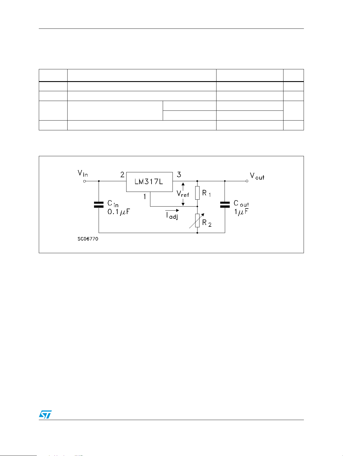
The LM317L provides an internal reference voltage of 1.25V between the output and
adjustments terminals. This is used to set a constant current flow across an external resistor
divider (see Figure 4.), giving an output voltage V
V
O
= V
(1 + R2/R1) + I
REF
ADJ R2
The device was designed to minimize the term I
constant with line and load changes. Usually, the error term I
obtain the previous requirement, all the regulator quiescent current is returned to the output
terminal, imposing a minimum load current condition. If the load is insufficient, the output
voltage will rise.
Since the LM317L is a floating regulator and "sees" only the input-to-output differential
voltage, supplies of very high voltage with respect to ground can be regulated as long as the
maximum input-to-output differential is not exceeded. Furthermore, programmable regulator
are easily obtainable and, by connecting a fixed resistor between the adjustment and output,
the device can be used as a precision current regulator. In order to optimize the load
regulation, the current set resistor R
(see Figure 4.) should be tied as close as possible to
1
the regulator, while the ground terminal of R
provide remote ground sensing.
of:
O
(100µA max) and to maintain it very
ADJ
should be near the ground of the load to
2
× R2 can be neglected. To
ADJ
9/18

Application circuits LM217L/LM317L
7 Application circuits
Figure 6. Basic adjustable regulator
Figure 7. Voltage regulator with protection diodes
Figure 8. Slow Turn-on 15V Regulator
10/18

LM217L/LM317L Application circuits
Figure 9. Current regulator
IO=V
REF/R1 + IADJ
Figure 10. 5V Electronic shut-down regulator
Figure 11. Digitally selected outputs
= 1.25V/R
1
(R2 = sets maximum VO)
11/18

Package mechanical data LM217L/LM317L
8 Package mechanical data
In order to meet environmental requirements, ST offers these devices in ECOPACK®
packages. These packages have a Lead-free second level interconnect. The category of
second Level Interconnect is marked on the package and on the inner box label, in
compliance with JEDEC Standard JESD97. The maximum ratings related to soldering
conditions are also marked on the inner box label. ECOPACK is an ST trademark.
ECOPACK specifications are available at: www.st.com.
12/18

LM217L/LM317L Package mechanical data
SO-8 MECHANICAL DATA
DIM.
A 1.35 1.75 0.053 0.069
A1 0.10 0.25 0.04 0.010
A2 1.10 1.65 0.043 0.065
B 0.33 0.51 0.013 0.020
C 0.19 0.25 0.007 0.010
D 4.80 5.00 0.189 0.197
E 3.80 4.00 0.150 0.157
e 1.27 0.050
H 5.80 6.20 0.228 0.244
h 0.25 0.50 0.010 0.020
L 0.40 1.27 0.016 0.050
k ˚ (max.)
ddd 0.1 0.04
MIN. TYP MAX. MIN. TYP. MAX.
mm. inch
8
0016023/C
13/18

Package mechanical data LM217L/LM317L
TO-92 MECHANICAL DATA
mm. mils
DIM.
MIN. TYP MAX. MIN. TYP. MAX.
A 4.32 4.95 170.1 194.9
b 0.36 0.51 14.2 20.1
D 4.45 4.95 175.2 194.9
E 3.30 3.94 129.9 155.1
e 2.41 2.67 94.9 105.1
e1 1.14 1.40 44.9 55.1
L 12.7 15.49 500.0 609.8
R 2.16 2.41 85.0 94.9
S1 0.92 1.52 36.2 59.8
W 0.41 0.56 16.1 22.0
α 5° 5°
14/18
0102782/D

LM217L/LM317L Package mechanical data
Tape & Reel SO-8 MECHANICAL DATA
mm. inch
DIM.
MIN. TYP MAX. MIN. TYP. MAX.
A 330 12.992
C 12.8 13.2 0.504 0.519
D 20.2 0.795
N 60 2.362
T 22.4 0.882
Ao 8.1 8.5 0.319 0.335
Bo 5.5 5.9 0.216 0.232
Ko 2.1 2.3 0.082 0.090
Po 3.9 4.1 0.153 0.161
P 7.9 8.1 0.311 0.319
15/18

Package mechanical data LM217L/LM317L
Tape & Reel for TO-92 MECHANICAL DATA
DIM.
MIN. TYP MAX. MIN. TYP. MAX.
mm. inch
A1 4.80 0.189
T 3.80 0.150
T1 1.60 0.063
T2 2.30 0.091
d 0.48 0.019
P0 12.5 12.9 0.492 0.508
P2 5.65 7.05 0.222 0.278
F1, F2 2.44 2.54 2.94 0.096 0.100 0.116
delta H ±2 0.079
W 17.5 18.00 19.0 0.689 0.709 0.748
W0 5.7 6.3 0.224 0.248
W1 8.5 9.25 0.335 0.364
W2 0.50 0.20
H 18.50 18.70 0.728 0.726
H0 15.50 16.50 0.610 0.650
H1 25.00 0.984
D0 3.8 4.2 0.150 0.165
t 0.90 0.035
L1 3 0.118
delta P ±1 0.039
u 50 1.968
Φ1 360 14.173
Φ2 30 1.181
H1
delta P
A1
delta H
H
H0
L
d
W2
T
T2
T1
16/18
Φ1
Φ2
Pull-out direction
l1
W
W0
W1
F1
F2
P2
P0
D0
t
u
DRAWING NOT IN SCALE

LM217L/LM317L Revision history
9 Revision history
Table 4. Revision history
Date Revision Changes
16-Mar-2005 2 Add Tape & reel for TO-92.
23-Dec-2005 3 Mistake on ordering table in header.
18-May-2007 4 Order codes has been updated and the document has been reformatted.
17/18

LM217L/LM317L
Please Read Carefully:
Information in this document is provided solely in connection with ST products. STMicroelectronics NV and its subsidiaries (“ST”) reserve the
right to make changes, corrections, modifications or improvements, to this document, and the products and services described herein at any
time, without notice.
All ST products are sold pursuant to ST’s terms and conditions of sale.
Purchasers are solely responsible for the choice, selection and use of the ST products and services described herein, and ST assumes no
liability whatsoever relating to the choice, selection or use of the ST products and services described herein.
No license, express or implied, by estoppel or otherwise, to any intellectual property rights is granted under this document. If any part of this
document refers to any third party products or services it shall not be deemed a license grant by ST for the use of such third party products
or services, or any intellectual property contained therein or considered as a warranty covering the use in any manner whatsoever of such
third party products or services or any intellectual property contained therein.
UNLESS OTHERWISE SET FORTH IN ST’S TERMS AND CONDITIONS OF SALE ST DISCLAIMS ANY EXPRESS OR IMPLIED
WARRANTY WITH RESPECT TO THE USE AND/OR SALE OF ST PRODUCTS INCLUDING WITHOUT LIMITATION IMPLIED
WARRANTIES OF MERCHANTABILITY, FITNESS FOR A PARTICULAR PURPOSE (AND THEIR EQUIVALENTS UNDER THE LAWS
OF ANY JURISDICTION), OR INFRINGEMENT OF ANY PATENT, COPYRIGHT OR OTHER INTELLECTUAL PROPERTY RIGHT.
UNLESS EXPRESSLY APPROVED IN WRITING BY AN AUTHORIZED ST REPRESENTATIVE, ST PRODUCTS ARE NOT
RECOMMENDED, AUTHORIZED OR WARRANTED FOR USE IN MILITARY, AIR CRAFT, SPACE, LIFE SAVING, OR LIFE SUSTAINING
APPLICATIONS, NOR IN PRODUCTS OR SYSTEMS WHERE FAILURE OR MALFUNCTION MAY RESULT IN PERSONAL INJURY,
DEATH, OR SEVERE PROPERTY OR ENVIRONMENTAL DAMAGE. ST PRODUCTS WHICH ARE NOT SPECIFIED AS "AUTOMOTIVE
GRADE" MAY ONLY BE USED IN AUTOMOTIVE APPLICATIONS AT USER’S OWN RISK.
Resale of ST products with provisions different from the statements and/or technical features set forth in this document shall immediately void
any warranty granted by ST for the ST product or service described herein and shall not create or extend in any manner whatsoever, any
liability of ST.
ST and the ST logo are trademarks or registered trademarks of ST in various countries.
Information in this document supersedes and replaces all information previously supplied.
The ST logo is a registered trademark of STMicroelectronics. All other names are the property of their respective owners.
© 2007 STMicroelectronics - All rights reserved
STMicroelectronics group of companies
Australia - Belgium - Brazil - Canada - China - Czech Republic - Finland - France - Germany - Hong Kong - India - Israel - Italy - Japan -
Malaysia - Malta - Morocco - Singapore - Spain - Sweden - Switzerland - United Kingdom - United States of America
www.st.com
18/18
 Loading...