

现货库存、技术资料、百科信息、热点资讯,精彩尽在鼎好!
■ Wide single-supply voltage range or dual
supplies: +2V to +36V or ±1V to ±18V
■ Very low supply current (0.4mA) independent
of supply voltage (1mW/comparator at +5V)
■ Low input bias current: 25nA typ.
■ Low input offset current: ±5nA typ.
■ Low input offset voltage: ±1mV typ.
■ Input common-mode voltage range includes
ground
■ Low output saturation voltage: 250mV typ. (Io =
4mA)
■ Differential input voltage range equal to the
supply voltage
■ TTL, DTL, ECL, MOS, CMOS compatible
outputs
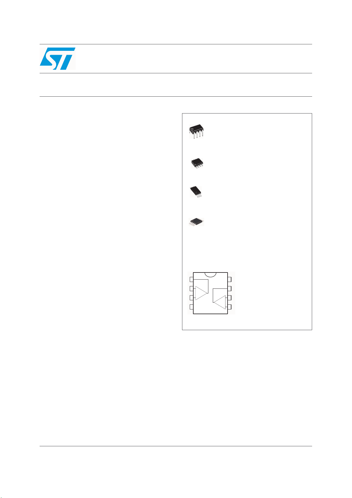
LM193, LM193A, LM293,
LM293A, LM393, LM393A
Low Power Dual Voltage Comparators
N
DIP8
(Plastic Package)
D
SO-8
(Plastic Micropackage)
P
TSSOP8
(Thin Shrink Small Outline Package)
S
Mini SO-8
(Plastic Micropackage)
Description
These devices consist of two independent low
voltage comparators designed specifically to
operate from a single supply over a wide range of
voltages. Operation from split power supplies is
also possible.
These comparators also have a unique
characteristic in that the input common-mode
voltage range includes ground even though
operated from a single power supply voltage.
Pin connections (top view)
1 - Output 1
1
2
-
+
3
45
2 - Inverting input 1
8
3 - Non-inverting input 1
7
4 - V
5 - Non-inverting input 2
6
-
6 - Inverting input 2
+
7 - Output 2
8 - V
CC
CC
-
+
February 2006 Rev. 6 1/15
www.st.com
15
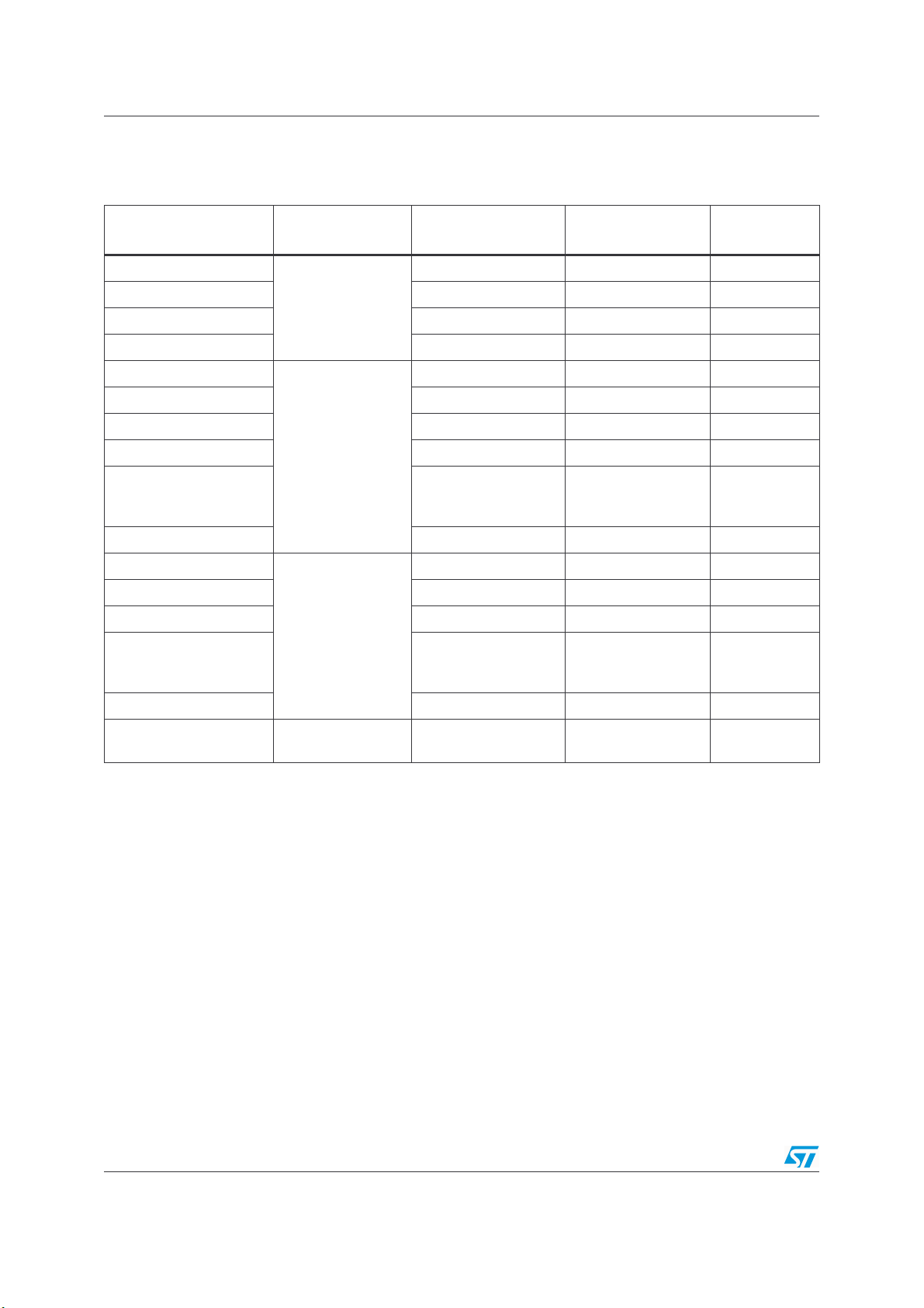
Order Codes LM193, LM193A, LM293, LM293A, LM393, LM393A
1 Order Codes
Part Number
LM193AD/LM193ADT
LM193AN DIP8 Tube
LM193D/LM193DT SO-8 Tube or Tape & Reel
LM193N DIP8 Tube
LM293AD/LM293ADT
LM293AN DIP8 Tube
LM293D/LM293DT SO-8 Tube or Tape & Reel
LM293N DIP8 Tube
LM293PT
LM293ST Mini SO-8 Tape & Reel
LM393AD/LM393ADT
LM393D/LM393DT SO-8 Tube or Tape & Reel
LM393N DIP8 Tube
LM393PT
Temperature
Range
-55°C, +125°C
-40°C, +105°C
0°C, +70°C
Package Packing Marking
SO-8 Tube or Tape & Reel
SO-8 Tube or Tape & Reel
TSSOP8
(Thin Shrink Outline
Package)
SO-8 Tube or Tape & Reel
TSSOP8
(Thin Shrink Outline
Package)
Tape & Reel
Tape & Reel
LM393ST Mini SO-8 Tape & Reel
LM393YDT/YD -40°C, +125°C
SO-8 (automotive
grade level)
Tube or Tape & Reel
2/15
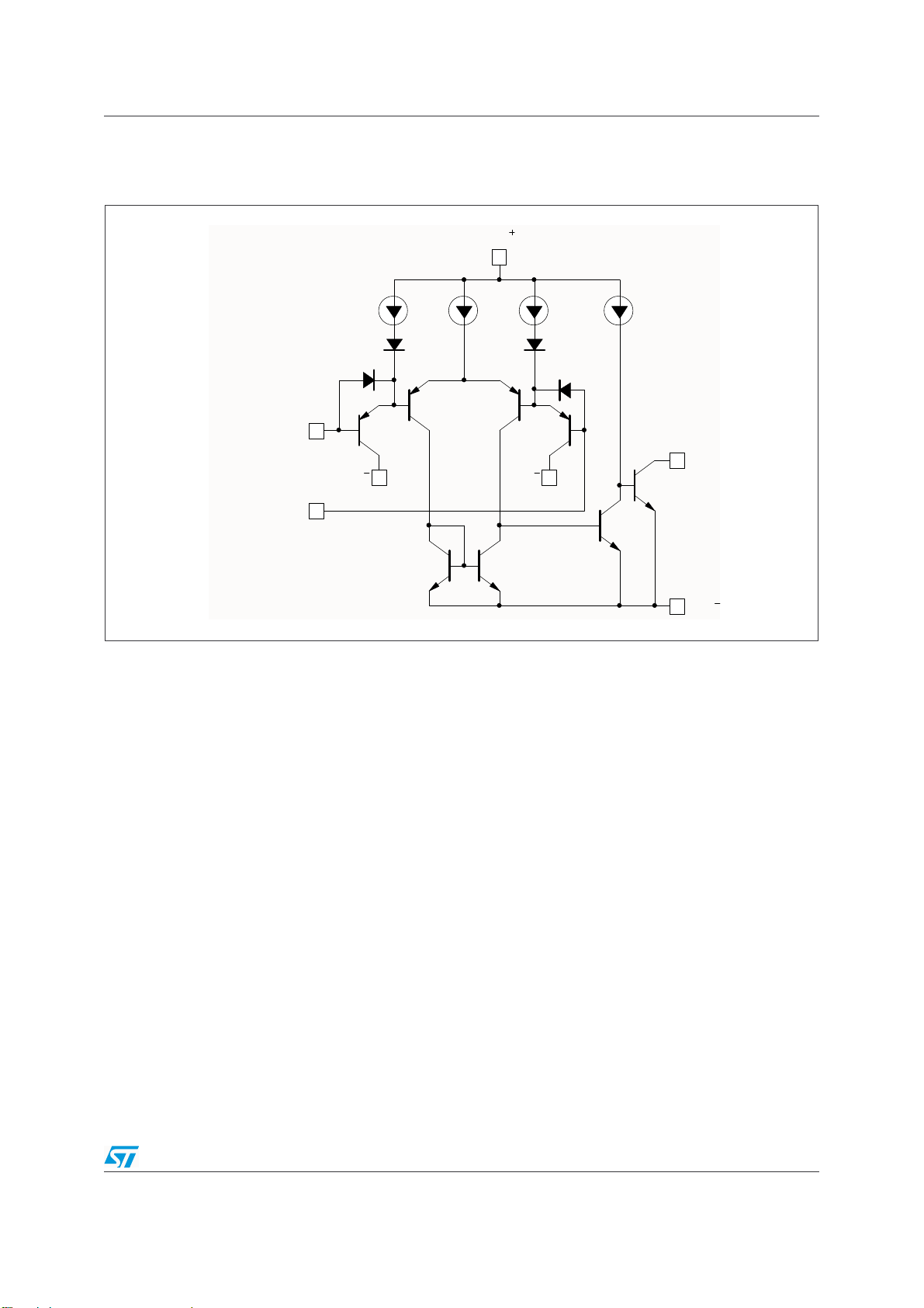
LM193, LM193A, LM293, LM293A, LM393, LM393A Schematic Diagram (1/2 LM193)
Non-inverting
Input
Inverting
Input
3.5µA 100µA 3.5µA 100µA
CC
V
CC
V
CC
V
CC
V
O
V
2 Schematic Diagram (1/2 LM193)
3/15
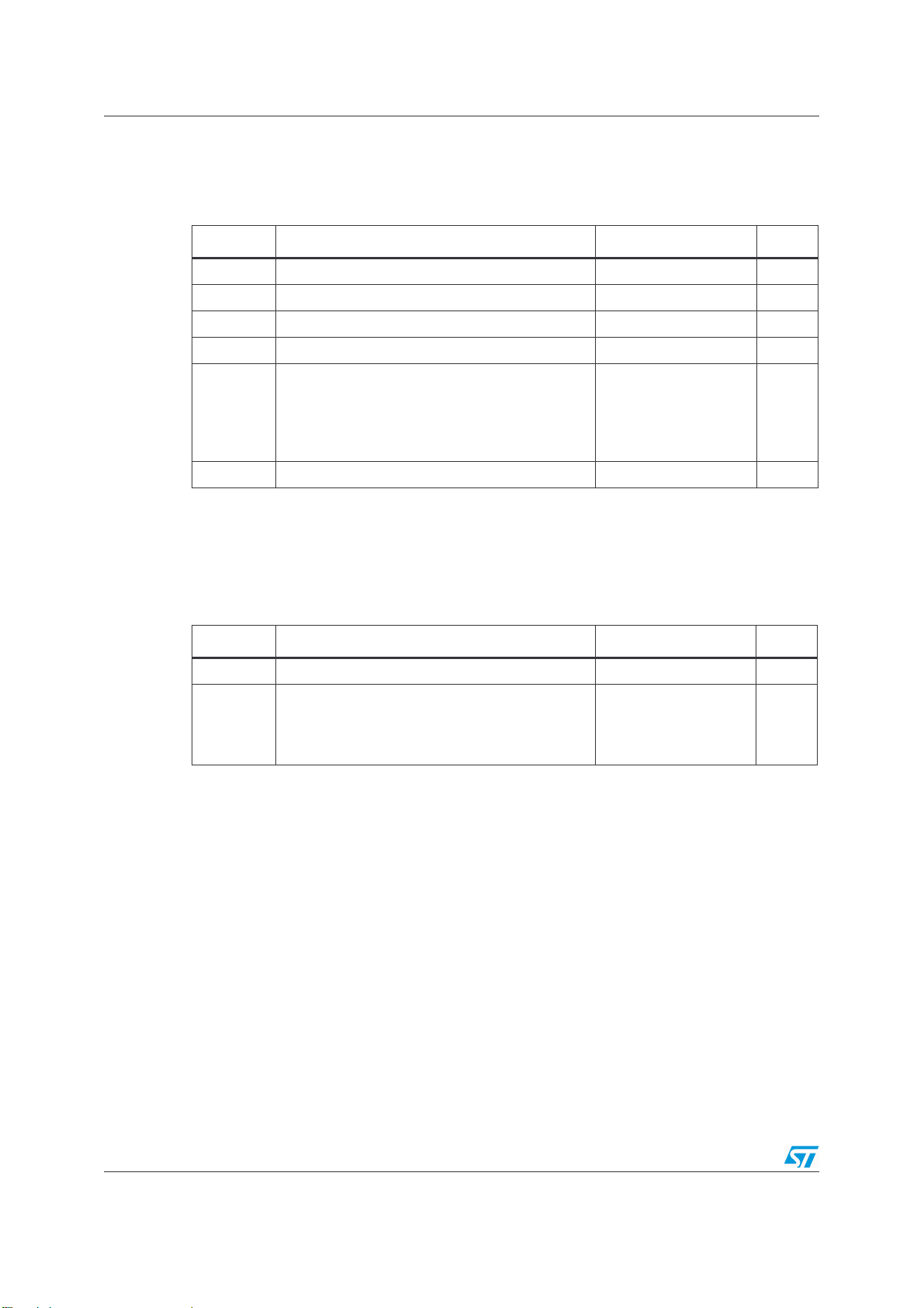
Absolute Maximum Ratings LM193, LM193A, LM293, LM293A, LM393, LM393A
3 Absolute Maximum Ratings
Table 1. Key parameters and their absolute maximum ratings
Symbol Parameter Value Unit
V
CC
V
Supply Voltage ±18 or 36 V
Differential Input Voltage ±36 V
id
Vi Input Voltage -0.3 to +36 V
Output Short-circuit to Ground - note
Power Dissipation
(2)
DIP-8
P
d
SO-8
TSSOP8
Mini SO-8
T
stg
1. Short-circuits from the output to V
maximum output current is approximately 20mA independent of the magnitude of V
2. Pd is calculated with T
R
thja
R
thja
R
thja
R
thja
Table 2. Operating conditions
Storage Temperature Range -65 to +150 °C
+
can cause excessive heating and eventual destruction. The
CC
= +25°C, Tj = +150°C and
= 100°C/W for DIP8 package
= 175°C/W for SO-8 package
= 200°C/W for TSSOP8 package
= 215°C/W for Mini SO-8 package
amb
(1)
Infinite
1250
710
625
580
CC
+
.
Symbol Parameter Value Unit
V
icm
Common Mode Input Voltage Range 0 to V
+
-1.5 V
CC
Operating Free-Air Temperature range
T
oper
LM193, A
LM293, A
LM393, A
-55 to +125
-40 to +105
0 to +70
mW
°C
4/15
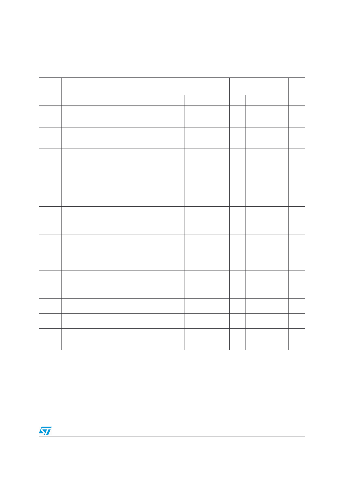
LM193, LM193A, LM293, LM293A, LM393, LM393A Electrical Characteristics
4 Electrical Characteristics
Table 3. V
+
= +5V, V
CC
Symbol Parameter
CC
-
= 0V, T
= +25°C (unless otherwise specified)
amb
LM193A - LM293A
LM393A
LM193- LM293
LM393
Unit
Min. Typ. Max. Min Typ. Max.
Input Offset Voltage - note
V
T
T
amb
min
= +25°C
≤ T
amb
io
≤ T
max
(1)
12
159mV
4
Input Offset Current
T
T
amb
min
= +25°C
≤ T
amb
≤ T
max
I
io
Input Bias Current (I+ or I-) - note
T
I
ib
A
vd
= +25°C
amb
T
≤ T
min
Large Signal Voltage Gain
V
CC
≤ T
amb
= 15V, RL = 15kΩ, Vo = 1V to 11V 50 200 50 200
max
(2)
325
100
25 100
300
550
150
25 250
400
V/mV
Supply Current (all comparators)
I
V
CC
V
icm
V
id
= +5V, no load
CC
V
= +30V, no load
CC
Input Common Mode Voltage Range - note
V
= 30V
CC
T
= +25°C
amb
T
≤ T
amb
≤ T
max
(4)
min
Differential Input Voltage -note
(3)
0.4
1
0
0
1
2.5
+
V
-1.5
CC
+
V
-2
CC
+
V
CC
0.4
1
0
0
1
2.5
+
-1.5
V
CC
+
V
-2
CC
+
V
CC
Low Level Output Voltage
V
= -1V, I
V
I
OH
I
SINK
tre
OL
id
T
= +25°C
amb
T
≤ T
min
High Level Output Current (Vid = 1V)
V
= Vo = 30V
CC
T
= +25°C
amb
T
≤ T
min
Output Sink Current
V
= 1V, Vo = 1.5V 6 16 6 16
id
Response Time - note
R
= 5.1kΩ connected to V
L
Large Signal Response Time
trel
R
= 5.1kΩ connected to V
L
V
= +1.4v 300 300
(ref)
1. At output switch point, Vo ≈ 1.4V, Rs = 0 with V
1.5V).
2. The direction of the input current is out of the IC due to the PNP input stage. This current is essentially constant,
independent of the state of the output, so no loading charge exists on the reference of input lines.
3. The input common-mode voltage of either input signal voltage should not be allowed to go negative by more than 0.3V. The
upper end of the common-mode voltage range is V
4. The response time specified is for a 100mV input step with 5mV overdrive. For larger overdrive signals 300ns can be
obtained.
5. Positive excursions of input voltage may exceed the power supply level. As long as the other voltage remains within the
common-mode range, the comparator will provide a proper output state. The low input voltage state must not be less than -
0.3V (or 0.3V bellow the negative power supply, if used).
amb
amb
sink
≤ T
≤ T
= 4mA
max
max
(5)
CC
CC
+
+,
el = TTL,
250 400
250 400
700
0.1
0.1
1
1.3 1.3
+
from 5V to 30V, and over the full common-mode range (0V to V
CC
+
-1.5V, but either or both inputs can go to +30V without damage.
CC
700
1
CC
+
-
nA
nA
mA
V
mV
nA
µA
mA
µs
ns
5/15

Electrical Characteristics LM193, LM193A, LM293, LM293A, LM393, LM393A
Figure 1. Supply current vs. supply voltage Figure 2. Input current vs. supply voltage
1
T
=-55°C
amb
T
T
amb
amb
T
amb
= +25°C
0.8
0.6
0.4
T
= +125°C
amb
0.2
SUPPLY CURRENT (mA)
0
10 20 30 40
R
SUPPLY VOLTAGE (V)
Figure 3. Output saturation voltage vs.
frequency
1
10
Out of saturation
Out of saturation
0
10
T
= +125°C
amb
T
=-55°C
amb
T
=+25°C
amb
10
-1
10
0
10
1
OUTPUT SINK CURRENT (mA)
SATURATION VOLTAGE (V)
10
10
10
-1
-2
-3
10
-2
=0°C
=+70°C
=
10
80
V=0V
i
60
40
R=10
i
T
amb
9
Ω
=0°C
T
=+25°C
amb
T
amb
= -55°C
20
T
= +125°C
INPUTCURRENT(nA)
amb
T
0
10 20 30 40
SUPPLY VOLTAGE (V)
Figure 4. Response time for various input
overdrives - negative transition
6
5
4
3
2
1
0
0
INPUT VOLTAGE (mV)
-50
OUTPUT VOLTAGE (V)
-100
2
Input overdrive : 5mV
20mV
100mV
T
amb
0 0.5 1 1.5 2
TIME (
s)
µ
amb
e
I
=+25°C
=+70°C
5V
5.1k
e
o
Ω
Figure 5. Response time for various input
overdrives - positive transition
6
1
INPUT VOLTAGE (mV)
OUTPUT VOLTAGE (V)
6/15
pIn ut overdrive : 100mV
5
4
3
2
1
20mV
0
00
T
=+25°C
50
amb
0
0 0.5 1 1.5 2
TIME (
µ
5mV
s)
5V
Ω
5.1k
e
I
e
o

LM193, LM193A, LM293, LM293A, LM393, LM393A Electrical Characteristics
4.1 Typical applications
Figure 6. Basic comparator Figure 7. Driving TTL
VCC=5V
15k
Ω
+V
-V
(ref)
(ref)
1/2
LM193
V
O
Figure 8. Low frequency op-amp Figure 9. Driving CMOS
(e = 0V for e = 0V)
o
~
e
1k
I
1/2
LM193
I
100k
W
A = 100
V
W
5V
15k
0.5mF
W
2N 2222
e
o
+V
-V
(ref)
(ref)
+V
-V
1/2
LM193
(ref)
1/2
LM193
(ref)
5V
5V
10k
W
100k
&
&
W
&
Figure 10. Low frequency op-amp Figure 11. Transducer amplifier
10k
5V
W
1/2
LM193
20M
3k
W
W
5V
W
15k
1/2
1k
LM193
e
I
W
100k
e
0.5mF
o
W
A = 100
V
~
Magnetic pick-up
10k
W
7/15
e
o

Electrical Characteristics LM193, LM193A, LM293, LM293A, LM393, LM393A
Figure 12. Low frequency op-amp with offset
adjust
5V
Offset Adjust
R2
R
s
~
e
I
R
1M
I
W
100k
W
1k
W
1M
15k
1/2
LM193
0.5mF
R1
100k
W
5V
W
2N 2222
W
Figure 13. Zero crossing detector
(single power supply)
100k
5.1k
5.1k
e
I
e
o
W
W
1N4148
5V
W
10k
100k
W
1/2
LM193
20M
W
W
Figure 14. Limit comparator Figure 15. Crystal controlled oscillator
(12V)
high
V
CC
10k
1/2
LM193
W
Lamp
2R
V
(ref)
S
R
S
200k
0.1mF
V
=15V
CC
W
100k
1/2
LM193
2k
W
W
V
CC
0
e
o
5.1k
W
~
e
I
1/2
V
low
2R
(ref)
LM193
S
2N 2222
Figure 16. Split-supply applications - zero
crossing detector
15V
W
5.1k
1/2
LM193
~
e
I
e
o
15V
f = 100kHz
W
200k
Figure 17. Comparator with a negative
reference
15V
5.1k
1/2
LM193
~
e
I
5V
15V
W
e
o
8/15

LM193, LM193A, LM293, LM293A, LM393, LM393A Electrical Characteristics
Figure 18. Two-decade high-frequency VCO
Frequency control
voltage input
v
control
100k
W
50k
W
V
CC
+250mV
700 Hz f 100kHz
0.1mF
20k
W
=+30V
V
o
control
20k
1/2
LM193
W
+50V
500pF
V
1/2
LM193
CC
W
3k
5.1k
0.01mF
100k
CC
W
3k
V
W
W
1/2
LM193
V
/2
CC
V
/2
CC
Output 1
Output 2
9/15

Package Mechanical Data LM193, LM193A, LM293, LM293A, LM393, LM393A
5 Package Mechanical Data
In order to meet environmental requirements, ST offers these devices in ECOPACK®
packages. These packages have a Lead-free second level interconnect. The category of
second level interconnect is marked on the package and on the inner box label, in
compliance with JEDEC Standard JESD97. The maximum ratings related to soldering
conditions are also marked on the inner box label. ECOPACK is an ST trademark.
ECOPACK specifications are available at: www.st.com
5.1 DIP8 package
Plastic DIP-8 MECHANICAL DATA
.
DIM.
A 3.3 0.130
a1 0.7 0.028
B 1.39 1.65 0.055 0.065
B1 0.91 1.04 0.036 0.041
b 0.5 0.020
b1 0.38 0.5 0.015 0.020
D 9.8 0.386
E 8.8 0.346
e 2.54 0.100
e3 7.62 0.300
e4 7.62 0.300
F 7.1 0.280
I 4.8 0.189
L 3.3 0.130
Z 0.44 1.6 0.017 0.063
MIN. TYP MAX. MIN. TYP. MAX.
mm. inch
10/15
P001F

LM193, LM193A, LM293, LM293A, LM393, LM393A Package Mechanical Data
5.2 SO8 package
SO-8 MECHANICAL DATA
DIM.
A 1.35 1.75 0.053 0.069
A1 0.10 0.25 0.04 0.010
A2 1.10 1.65 0.043 0.065
B 0.33 0.51 0.013 0.020
C 0.19 0.25 0.007 0.010
D 4.80 5.00 0.189 0.197
E 3.80 4.00 0.150 0.157
e 1.27 0.050
H 5.80 6.20 0.228 0.244
h 0.25 0.50 0.010 0.020
L 0.40 1.27 0.016 0.050
k ˚ (max.)
ddd 0.1 0.04
MIN. TYP MAX. MIN. TYP. MAX.
mm. inch
8
0016023/C
11/15

Package Mechanical Data LM193, LM193A, LM293, LM293A, LM393, LM393A
5.3 TSSOP8 package
TSSOP8 MECHANICAL DATA
DIM.
A 1.2 0.047
A1 0.05 0.15 0.002 0.006
A2 0.80 1.00 1.05 0.031 0 .039 0.041
b 0.19 0.30 0.007 0.012
c 0 .09 0.20 0.004 0.008
D 2.90 3.00 3.10 0.114 0 .118 0.122
E 6.20 6.40 6.60 0.244 0 .252 0.26 0
E1 4.30 4.40 4.50 0.169 0 .173 0.177
e 0.65 0.0256
K0˚ 8˚0˚ 8˚
L 0.45 0.60 0.75 0.01 8 0.024 0.030
L1 1 0.039
MIN. TYP MAX. MIN. TYP. MAX.
mm. inch
12/15
0079397/D

LM193, LM193A, LM293, LM293A, LM393, LM393A Package Mechanical Data
5.4 MiniSO8 package
13/15

Revision History LM193, LM193A, LM293, LM293A, LM393, LM393A
6 Revision History
Table 4. Document revision history
Date Revision Changes
July 2002 1 First Release
Jan. 2005 2 Class A of the product included in the datasheet.
May 2005 3
July 2005 4
Nov. 2005 5
Feb. 2006 6 Unit error for Vol parameter see
PPAP references inserted in the datasheet see
page 2
.
Modification on PPAP references - Errors on part numbers see
Table 1 on page 2
Modification on
40/+105°C instead of -40/+125°C.
.
Table 3 on page 5
Table 1 on
. LM293,A must be -
Table 3 on page 5
.
14/15

LM193, LM193A, LM293, LM293A, LM393, LM393A Revision History
y
y
Please Read Carefully:
Informatio n in this document is provided solely in connection with ST products. STMicroelectronics NV and its subsidiaries (“ST”) reserve the
right to make changes, corrections, modifications or improvements, to this document, and the products and services described herein at an
time, without notice.
All ST products are sold pu rsuant to ST’s terms and conditions of sale.
Purchasers are solely responsible for the choice, selection and use of the ST products and services described herein, and ST assumes no
liability whatsoever relating to the choice, selection or use of the ST products and services described herein.
No license, express or implied, by estoppel or otherwise, to any intellectual property rights is granted under this document. If any part of this
document refers to any third party products or services it shall not be deemed a license grant by ST for the use of such third party products
or services, or any intellectual property contained therein or considered as a warranty covering the use in any manner whatsoever of such
third party products or services or any intellectual property contained therein.
UNLESS OTHERWISE SET FORTH IN ST’S TERMS AND CONDITIONS OF SALE ST DISCLAIMS ANY EXPRESS OR IMPLIED
WARRANTY WITH RESPECT TO THE USE AND/OR SALE OF ST PRODUCTS INCLUDING WITHOUT LIMITATION IMPLIED
WARRANTIES OF MERCHANTABILITY, FITNESS FOR A PARTICULAR PURPOSE (AND THEIR EQUIVALENTS UNDER THE LAWS
OF ANY JURISDICTION), OR INFRINGEMENT OF ANY PATENT, COPYRIGHT OR OTHER INTELLECTUAL PROPERTY RIGHT.
UNLESS EXPRESSLY APPROVED IN WRITING BY AN AUTHORIZE REPRESENTATIVE OF ST, ST PRODUCTS ARE NOT DESIGNED,
AUTHORIZED OR WARRANTED FOR USE IN MILITARY, AIR CRAFT, SPACE, LIFE SAVING, OR LIFE SUSTAINING APPLICATIONS,
NOR IN PRODUCTS OR SYSTEMS, WHERE FAILURE OR MALFUNCTION MAY RESULT IN PERSONAL INJURY, DEATH, OR
SEVERE PROPERTY OR ENVIRONMENTAL DAMAGE.
Resale of ST products with provisions different from the statements and/or technical features set forth in this document shall immediately void
any warranty granted by ST for the ST product or service described herein and shall not create or extend in any manner whatsoever, an
liability of ST.
ST and the ST logo are trademarks or registered trademarks of ST in various countries.
Information in this document supersedes and replaces all information previously supplied.
The ST logo is a registered trademark of STMicroelectronics. All other names are the property of their respective owners.
© 2006 STMicroelectronics - All rights reserved
STMicroelectronics group of companies
Australia - Belgium - Brazil - Canada - China - Czech Republic - Finland - France - Germany - Hong Kong - India - Israel - Italy - Japan -
Malaysia - Malta - Morocco - Singapore - Spain - Sweden - Switzerland - United Kingdom - United States of America
www.st.com
15/15
 Loading...