

LM148
LM248
LM348
FOUR UA741
QUAD BIPOLAR OPERATIONAL AMPLIFIERS
■ LOW SUPPLY CURRENT: 0.53mA/AMPLI-
FIER
■ CLASS AB OUTPUT STAGE: NO CROSS
OVER DIST ORTION
■ PIN COMPATIBLE WITH LM124
■ LOW INPUT OFFSET VOLTAGE: 1mV
■ LOW INPUT OFFSET CURRENT: 2nA
■ LOW INPUT BIAS CURRENT : 30nA
■ GAIN BANDWIDTH PRODUCT: 1.3MHz
■ HIGH DEGREE OF IS OLATION BETWEEN
AMPLIFIERS: 120dB
■ OVERLOAD PROT ECTION FOR INPUTS
AND OUTPUTS
DESCRIPTION
The LM148 consists of four independent, high
gain internally compensated, low power operational amplifiers which have been designed to provide functional characteristics identical to those of
the familiar UA741 operat ional amplifier. In addition the total supply current for all four amplifiers is
compatible to the supply current of a single UA741
type op amp. Other features inclu de inpu t of fset
current and input bias current which are much less
than those of a standard UA741. Also, excellent
isolation between amplifiers has been achieved by
independently biasing each amplifier and using
layout techniques qhich minimize thermal coupling.
The LM148 can be used anywhere multiple
UA741 type amplifiers are being used and in applications where amplifier matching or high packaing
density is required.
ORDER CODE
Part
Number
Temperature
Range
LM148 -55°C, +125°C
LM248 -40°C, +105°C
LM348 0°C, +70°C
Example : LM348D
Package
ND
••
••
••
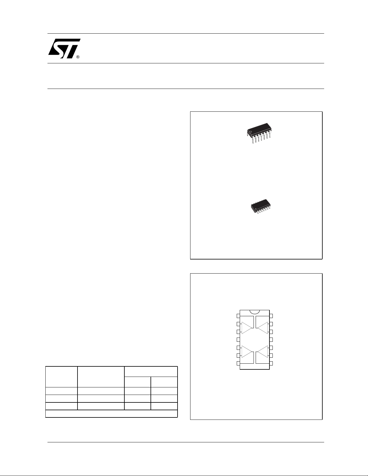
N
DIP14
(Plastic Package)
D
(Plastic Micropackage)
PIN CONNECTIONS (top view)
1
Output 1
V
CC
Output 2
2
3
+
4
5
6
7
Inverting Input 1
Non-inverting Input 1
Non-inverting Input 2
Inverting Input 2
SO14
14
13
-
+
+
-
-
+
12
11
10
+
9
8
Output 4
Inverting Input 4
Non-inverting Input 4
-
V
CC
Non-inverting Input 3
Inverting Input 3
Output 3
N = Dual in Line Package (DIP)
D = Small Outline Package (SO) - also available i n Tape & Reel (DT)
March 2002
1/5
LM148-LM248-LM348
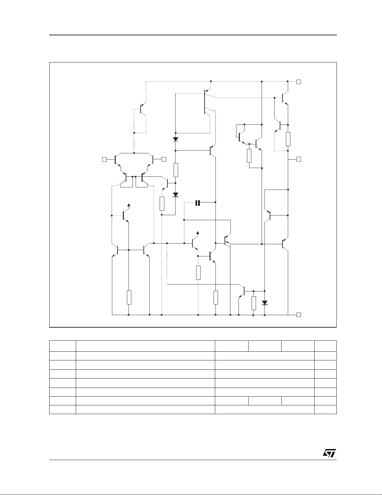
SCHEMATIC DIAGRAM
Non-inverting input
Inverting
input
Vcc+
25W
Output
350kW
Vcc+
2.5kW
60kW
7.4pF
Vcc+
60W
340W
36kW
Vcc-
ABSOLUTE MAXIMUM RATINGS
Symbol Parameter LM148 LM248 LM348 Unit
V
P
T
T
1. For supply voltage less than maximum value, the absolute maximum input voltage is equal to the supply voltage.
2. Any of the amplifier outputs can be shorted to ground indefinitly; however more than one should not be simultaneously shorted as the maximum
Supply voltage ±22 V
CC
V
Input Voltage
i
V
Differential Input Voltage ±44 V
id
Output Short-circuit Duration
Power Dissipation 500 mW
tot
Operating Free-air Temperature Range -55 to +125 -40 to +105 0 to +70 °C
oper
Storage Temperature Range -65 to +150 °C
stg
junction will be exceeded.
1)
2)
±22 V
Infinite
2/5

LM148-LM248-LM348
ELECTRICAL CHARACTERISTICS
V
= ±15V, T
CC
Symbol Parameter Min. Typ. Max. Unit
Input Offset Voltage (Rs ≤ 10kΩ)
V
io
Input Offset Current
I
io
Input Bias Current
I
ib
Large Signal Voltage Gain (Vo = ±10V, RL = 2k
A
vd
Supply Voltage Rejection Ratio (R
SVR
Supply Current, all Amp, no load
I
cc
Input Common Mode Voltage Range
V
icm
Common Mode Rejection Ratio (R
CMR
Output Short-circuit Current
I
os
Output Voltage Swing
±V
opp
Slew Rate (V
SR
Rsie Time (VI = ±10V, RL = 10kΩ, CL = 100pF, unity Gain)
t
r
Overshoot (VI = ±10V, RL = 10kΩ, CL = 100pF, unity Gain)
K
OV
R
Input Resistance 0.8 2.5 M
I
GBP
THD
V
o1/Vo2
Gain Bandwith Product (V
f =100kHz)
Total Harmonic Distortion (f = 1kHz, A
C
L
Equivalent Input Noise Voltage (f = 1kHz, Rs = 100
e
n
Channel Separation 120 dB
= 25°C (unless otherwise specified)
amb
T
T
T
T
T
T
amb
min
amb
min
amb
min
= 25°C
≤ T
amb
= 25°C
≤ T
amb
= 25°C
≤ T
amb
≤ T
≤ T
≤ T
max
max
max
15
22575nA
30 100
Ω)
T
= 25°C
amb
T
≤ T
≤ T
amb
max
≤ 10kΩ)
s
= 25°C
≤ T
≤ T
amb
max
= 25°C
≤ T
≤ T
amb
max
= 25°C
≤ T
≤ T
amb
max
≤ 10kΩ)
s
= 25°C
≤ T
≤ T
amb
max
= 25°C
= 25°C RL ≤ 10k
≤ T
≤ T
amb
max
= ±10V, RL = 10kΩ, CL = 100pF, unity Gain)
I
T
T
T
T
T
T
T
T
min
amb
min
amb
min
amb
min
T
T
T
amb
min
amb
min
amb
R
≤ 2k
L
RL ≤ 10k
≤ 2k
R
L
Ω
Ω
Ω
Ω
50
160 V/mV
25
77
100 dB
77
2.1 3.6
±12
±12
70
110 dB
70
10 25 35
12
10
13
12 V
12
10
0.25 0.5 V/µs
0.3 µs
5%
= 10 mV, RL = 10kΩ, CL = 100pF
I
0.7 1.3
= 20dB, RL = 10k
v
Ω
= 100pF, Vo = 2Vpp) 0.08
Ω
40
6
300
4.8
MHz
----------- -
mV
nA
mA
mA
Ω
%
nV
Hz
3/5

LM148-LM248-LM348
PACKAGE MECHANICAL DATA
14 PINS - PLASTIC PACKAGE
Dimensions
Min. Typ. Max. Min. Typ. Max.
a1 0.51 0.020
B 1.39 1.65 0.055 0.065
b 0.5 0.020
b1 0.25 0.010
D 20 0.787
E 8.5 0.335
e 2.54 0.100
e3 15.24 0.600
F 7.1 0.280
i 5.1 0.201
L 3.3 0.130
Z 1.27 2.54 0.050 0.100
Millimeters Inches
4/5

PACKAGE MECHANICAL DATA
14 PINS - PLASTIC MICROPACKAGE (SO)
a2
LG
A
LM148-LM248-LM348
C
c1
b
e3
D
14
e
s
a1
b1
E
M
8
F
1
Dimensions
A 1.75 0.069
a1 0.1 0.2 0.004 0.008
a2 1.6 0.063
b 0.35 0.46 0.014 0.018
b1 0.19 0.25 0.007 0.010
C 0.5 0.020
c1 45° (typ.)
D (1) 8.55 8.75 0.336 0.344
E 5.8 6.2 0.228 0.244
e 1.27 0.050
e3 7.62 0.300
F (1) 3.8 4.0 0.150 0.157
G 4.6 5.3 0.181 0.208
L 0.5 1.27 0.020 0.050
M 0.68 0.027
S 8° (max.)
Note : (1) D and F do not i nclude mold flash or protrusions - Mold flash or protrusions shall not exceed 0.15mm (.066 inc) ONLY FOR DATA BOOK.
Information furnished is bel ieved to be accurate and reliable. However, STMicroe lectronics assumes no responsibility for the
consequences of use of such information nor for any infringement of patents or other rights of third parties which may result from
its use. No li cense is granted by implication or otherwise unde r any patent or patent rights of STMicroelectronics. Specifications
mentioned in this publication ar e subject to change without notice. This publication supersedes and replaces all information
previously supplied. S TMicroelectronics products are not authorized for use as critica l components in life suppo rt devices or
systems without express written approval of STMicroelectronics.
Min. Typ. Max. Min. Typ. Max.
Millimeters Inches
© The ST logo is a registered trademark of STMicroelectronics
7
© 2002 STM icroelectronics - Pr i n ted in Italy - A ll Rights Res er ved
STMicr o el ectronics GROUP OF COMPANI ES
Australi a - Brazil - Canada - Chin a - F i nl and - France - Germany - Hong Kong - Ind i a - Is rael - Italy - Japan - Malay sia
Malta - Mor occo - Singapore - Spain - Sweden - Switzerland - United Kingdom - Unit ed States
© http://www.st.com
5/5
 Loading...