

I
set
Vcc+Vcc
-– 0.6V–
R
set
-----------------------------------------------------=
LM146
LM246
LM346
PROGRAMMABLE
QUAD BIPOLAR OPERATIONAL AMPLIFIER
■ PROGR AMMAB L E ELECTRICAL CHARA C-
TERISTICS
■ LOW SUPPLY CURRENT (250µA/amplifier)
■ GAIN-BANDWITH PRODUCT : 1MHz
■ LARGE DC VOLT AGE GAIN : 120dB
■ LOW NOISE VOLTAGE : 28nV/√Hz
■ WIDE POWER SUPPLY RANGE / ±1.5V to
±22V
■ CLASSE AB OUTPUT STAGE. NO
CROSS-OVER DISTORTION
■ OVERLOAD PROT ECTION FOR INPUTS
AND OUTPUTS
DESCRIPTION
The LM346 consists of four independent, high
gain, internally compensated, low power programmable amplifiers. Two external resistors (R
low the user to program the gain-bandwith product, slew rate, supply current, input bias current,
input offset current and input noise. For example
the user can trade-off supply current for bandwith
or optimize noise figure for a given s ource resistance. In a similar way other amplifier characteristics can be tailored to the application.
Except for the two programming pins at the end of
the package the LM346 pin out is the same as the
LM324 and LM348.
set
) al-
N
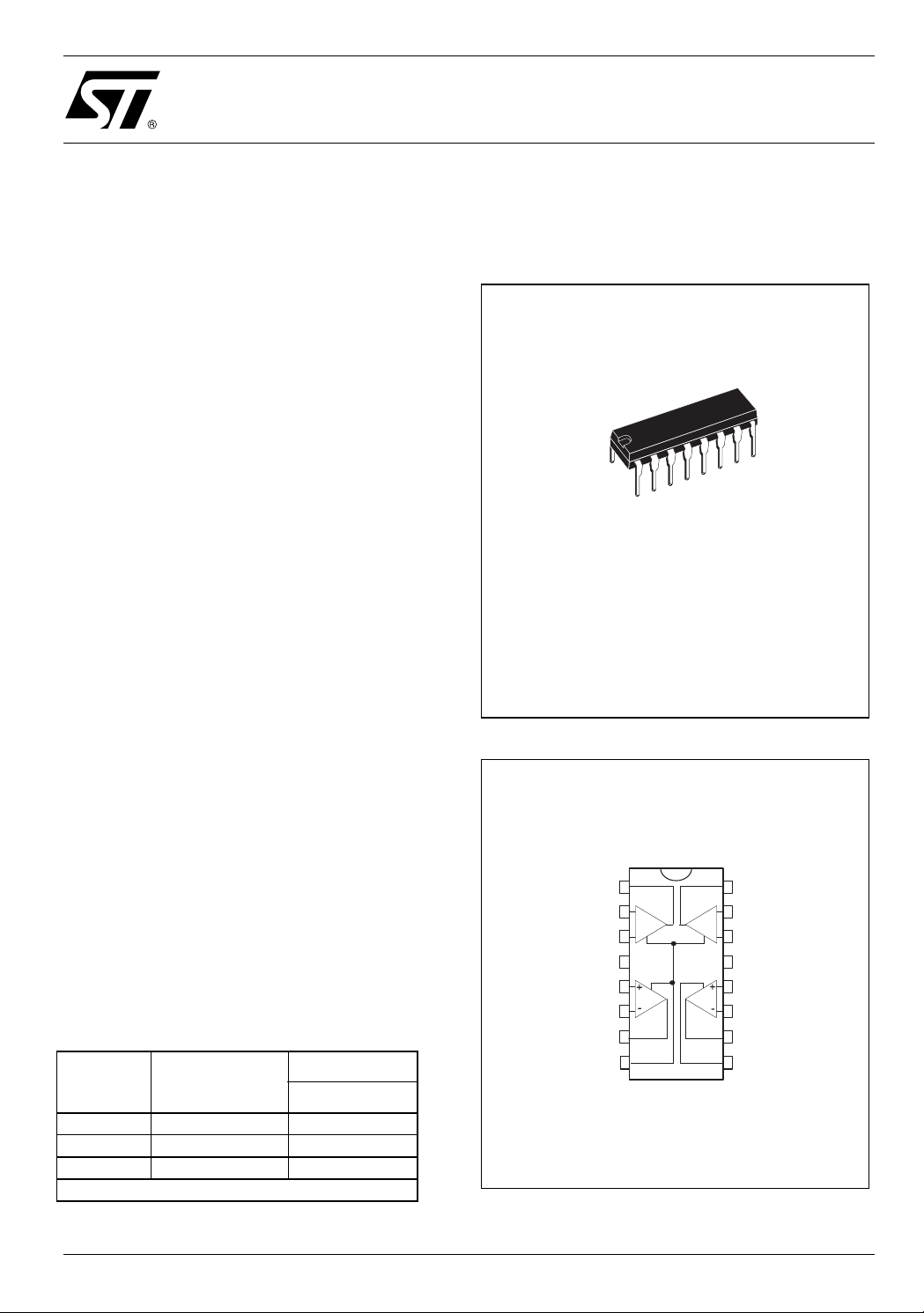
DIP16
(Plastic Package)
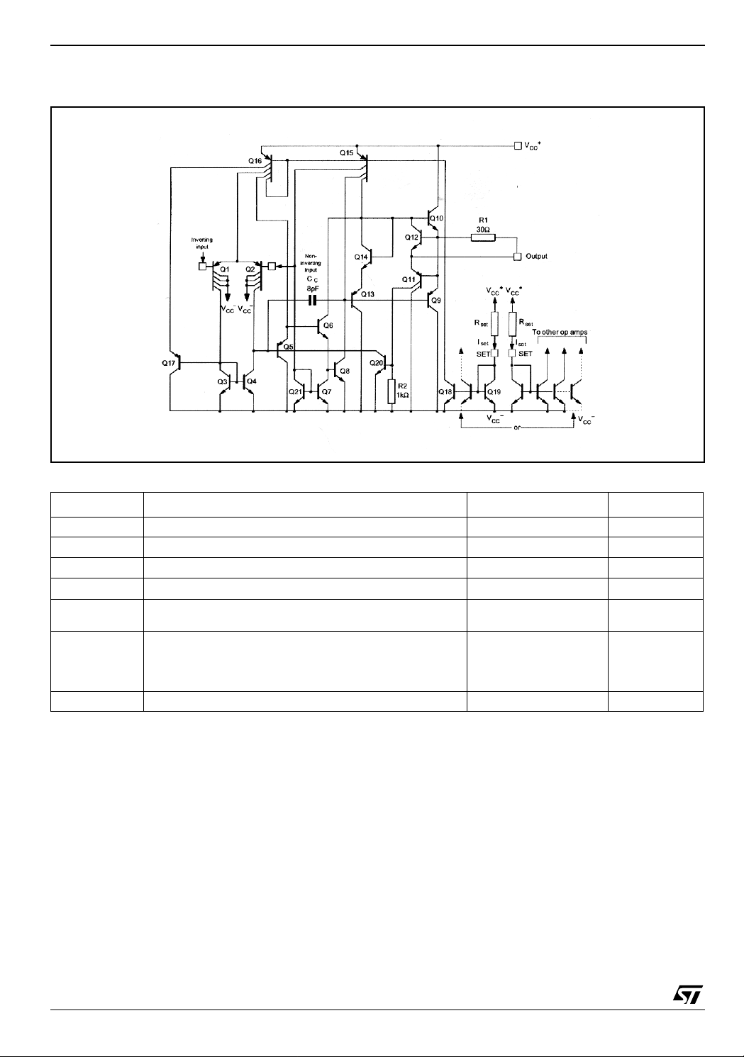
PIN CONNECTIONS (top view)
PROGRAMMING EQUATIONS :
Total supply current = 1mA (I
Gain bandwith product = 1MHz (I
Slew rate = 0.5V/µs (I
= 10µΑ)
set
Input bias current ≈30nA (I
I
= current into pi n 8 and pi n 9 (see schematic
set
set
= 10µΑ)
set
= 10µA)
= 10µA)
set
diagram)
ORDER CODE
Part
Number
Temperature
Range
LM146 -55°C, +125°C
LM246 -40°C, +105°C
LM346 0°C, +70°C
Example : LM246N
N = Dual in Line Package (DIP))
April 2003
Package
N
•
•
•
Output 1
Inverting Input 1
Non-inverting input 1
V
CC
Non-inverting Input 2
Inverting Input 2
Output 2
Set
Output 4
-
+
16
Inverting Input 4
15
Non-inverting input 4
14
-
13
V
CC
No n-inv erting in pu t 3
12
Inverting input 3
11
Output 3
10
Set
9
1
2
-
+
3
+
4
5
6
7
8
1/4
LM146-LM246-LM346
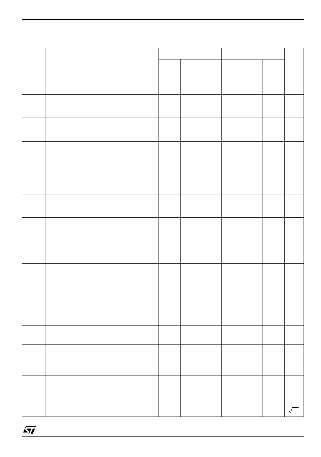
SCHEMATIC DIAGRAM (1/4 LM146)
ABSOLUTE MAXIMUM RATINGS
Symbol Parameter Value Unit
V
CC
V
i
V
id
P
tot
T
oper
T
stg
1. For supply voltage less than ±15V, the absolute maximum input voltage is equal to the supply voltage.
2. Any of the amplifier outputs can be shorted to ground indefinitly; however more than one should not be simultaneously shorted as the maximum
junction will be exceeded.
Supply voltage ±22 V
l Input Voltage
1)
±15 V
Differential Input Voltage ±30 V
Output Short-circu it Duration
2)
Power Dissipation 500
Infinite
mW
Opearting Free-air Temperature Range
LM146
LM246
LM346
-55 to +125
40 to +105
0 to +70-
°C
Storage Temperature Range -65 to +150 °C
2/4
ELECTRICAL CHARACTERISTICS
+
= ±15V, I
V
CC
Symbol Parameter
Input Offset Voltage (Rs ≤ 10kΩ)
V
io
Input Offset Current
I
io
Input Bias Current
I
ib
Large Signal Voltage Gain
A
vd
Supply Voltage Rejection Ratio (R
SVR
Supply Current, all Amp, no load
I
cc
Input Common Mode Voltage Range
V
icm
Common Mode Rejection Ratio (R
CMR
Output Short-circuit Current
I
os
Output Voltage Swing (RL ≤ 10kΩ)
±V
opp
Slew Rate (V
SR
unity Gain)
R
Input Resistance 1 1 M
I
C
Input Capacitance 2 2 pF
I
V
o1/Vo2
Channel Separation (RL = 10kΩ, Vo = 12Vpp)
Gain Bandwith Product
GBP
(V
f =100kHz)
Total Harmonic Distortion
THD
(f = 1kHz, A
C
Equivalent Input Noise Voltage
e
n
(f = 1kHz, R
= 10µA, T
set
T
= 25°C
amb
T
≤ T
min
amb
T
= 25°C
amb
T
≤ T
min
amb
T
= 25°C
amb
T
≤ T
min
amb
= ±10V, RL = 10k
(V
o
T
= 25°C
amb
T
≤ T
min
amb
T
= 25°C
amb
T
≤ T
min
amb
= 25°C
T
amb
T
≤ T
min
amb
= 25°C
T
amb
T
≤ T
min
amb
T
= 25°C
amb
T
≤ T
min
amb
= 25°C
T
amb
T
≤ T
min
amb
T
= 25°C
amb
T
≤ T
min
amb
= ±10V, RL = 10kΩ, CL = 100pF,
I
= 10 mV, RL = 10kΩ, CL = 100pF
I
= 20dB, RL = 10k
= 100pF, Vo = 2Vpp) 0.015 0.015
L
v
= 100
s
= +25°C (unless otherwise specified)
amb
≤ T
max
≤ T
max
≤ T
max
Ω)
≤ T
max
≤ T
max
≤ T
max
≤ T
max
≤ T
max
≤ T
max
≤ T
max
Ω
Ω
≤ 10kΩ)
s
≤ 10kΩ)
s
LM146-LM246-LM346
LM146 LM246 - LM346
Min. Typ. Max. Min. Typ. Max.
0.5 3
5
220
25
30 100
100
100501000 50251000
80
80
110 80
80
12
2
±13.5
±13.5
80
70
10
4
12
12
110 80
20 30
14 12
±13.5
±13.5
70
10
35
12
0.3 0.5 0.3 0.5
120 120 dB
0.8 1 0.5 1
28 28
4
0.5 5
2 100
100
30 250
250
110
12
110
20 30
35
14
6
V/mV
2
Unit
mV
nA
nA
dB
mA
dB
mA
V
V/µs
MHz
%
nV
----------- Hz
Ω
3/4
LM146-LM246-LM346
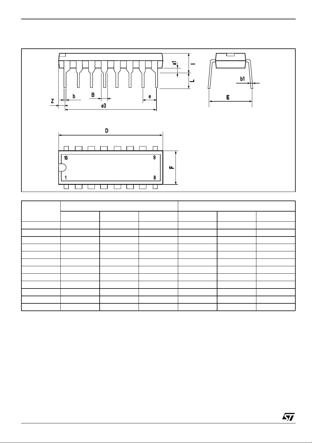
PACKAGE MECHANICAL DATA
16 PINS - PLASTIC PACKAGE
Dim.
Millimeters Inches
Min. Typ. Max. Min. Typ. Max.
a1 0.51 0.020
B 0.77 1.65 0.030 0.065
b 0.5 0.020
b1 0.25 0.010
D 20 0.787
E 8.5 0.335
e 2.54 0.100
e3 17.78 0.700
F 7.1 0.280
i 5.1 0.201
L 3.3 0.130
Z 1.27 0.050
Information furnished is bel ieved to be accurate and reliable. However, STMicroelec tronics assumes no responsibility for the
consequences of use of such information nor for any infringement of patents or other rights of third parties which may result from
its use. No li cense is granted by implication or otherwise under any patent or patent rights of STMicroelectronics. Specifications
mentioned in this publica tion are subject to change without notice. Thi s publication supersedes and replaces all information
previously supplied. STMicroelectronics products are not authorized for use as critical components in life support devices or
systems without express written approval of STMicroelectronics.
The ST logo is a registered trademark of STMicroelectronics
4/4
© 2003 STMicroelectronics - All Rights Reserved
STMicroelectronics GROUP OF COMPA NI ES
Australi a - Brazil - China - Finland - France - Germany - Hong Kong - India - Italy - Japan - M alaysia - Ma lta - Morocco
Singapo re - Spain - Sweden - Switzerl and - United Kingdom
http://www.st.com
 Loading...