


Three-terminal 5 A adjustable voltage regulators
Features
■ Guaranteed 7 A peak output current
■ Guaranteed 5 A output current
■ Adjustable output down to 1.2 V
■ Line regulation typically 0.005 %/V
■ Load regulation typically 0.1 %
■ Guaranteed thermal regulation
■ Current limit constant with temperature
■ Standard 3-lead transistor package
Description
The LM138, LM238, LM338 are adjustable 3terminal positive voltage regulators capable of
supplying in excess of 5 A over a 1.2 V to 32 V
output range. They are exceptionally easy to use
and require only 2 resistors to set the output
voltage. Careful circuit design has resulted in
outstanding load and line regulation comparable
to many commercial power supplies. The LM138
family is supplied in a standard 3-lead transistor
package.
A unique feature of the LM138 family is time-dependent current limiting. The current limit circuitry
allows peak currents of up to 12 A to be drawn
from the regulator for short periods of time. This
allows the LM138 to be used with heavy transient
loads and speeds start-up under full-load
conditions. Under sustained loading conditions,
the current limit decreases to a safe value
protecting the regulator. Also included on the chip
are thermal overload protection and safe area
protection for the power transistor. Overload
LM138 - LM238 - LM338
TO-3
protection remains functional even if the
adjustment pin is accidentally disconnected.
Normally, no capacitors are needed unless the
device is situated far from the input filter
capacitors in which case an input bypass is
needed. An optional output capacitor can be
added to improve transient response. The
adjustment terminal can be bypassed to
achieve.very high ripple rejection ratios which are
difficult to achieve with standard 3-terminal
regulators.
Besides replacing fixed regulators or discrete
designs, the LM238 is useful in a wide variety of
other applications. Since the regulator is "floating"
and sees only the input-to-output differential
voltage, supplies of several hundred volts can be
regulated as long as the maximum input to input
differential is not exceeded.
The LM138, LM238, LM338 are packaged in
standard steel TO-3 transistor package. The
LM138 is rated for operation from - 55 °C to
150 °C, the LM238 from - 25 °C to 150 °C and the
LM338 from 0 °C to 125 °C.
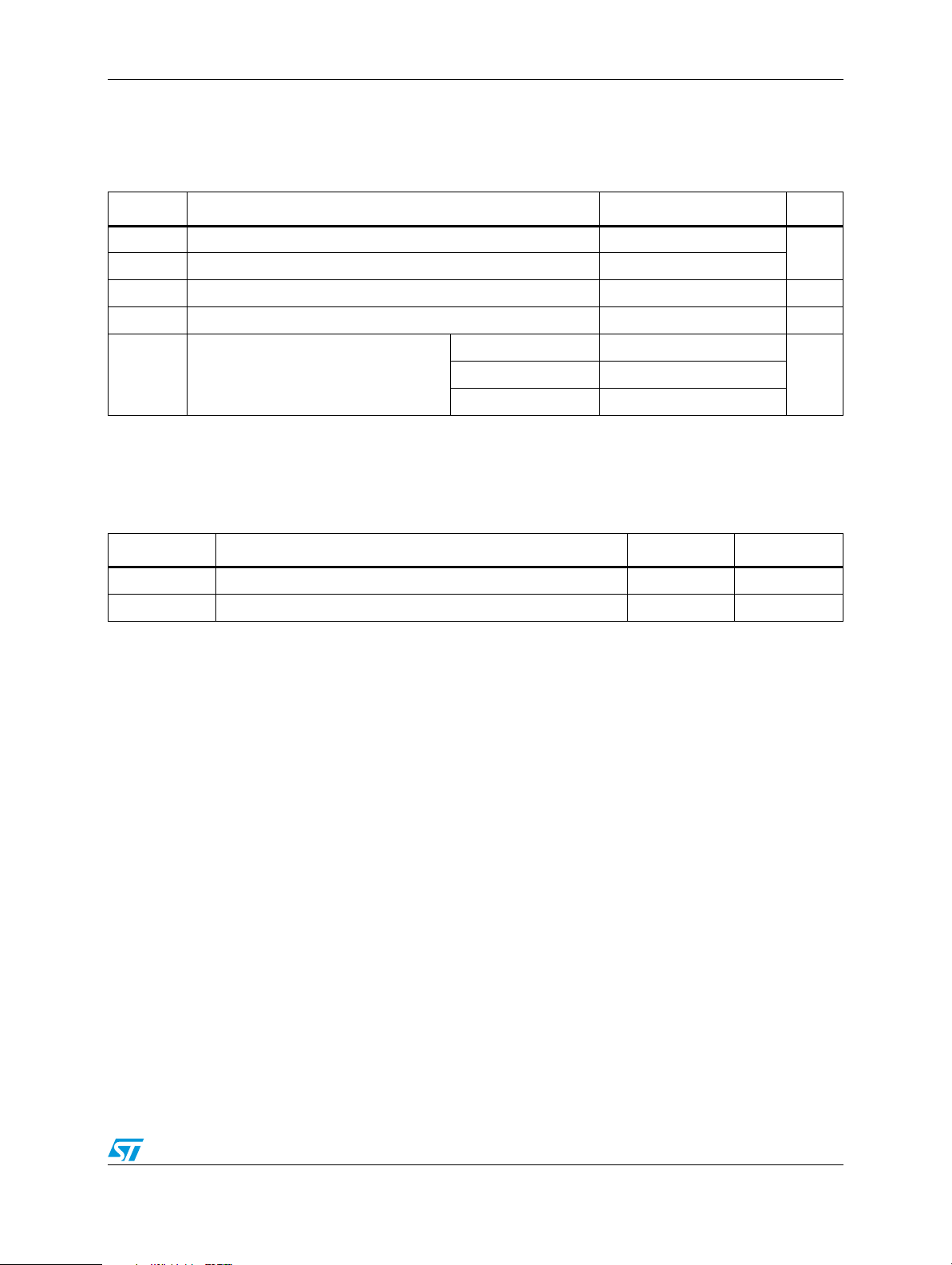
Table 1. Device summary
Part numbers Order codes Temperature range
LM138 LM138K -55 °C to 150 °C
LM238 LM238K -25 °C to 150 °C
LM338 LM338K 0 °C to 125 °C
April 2008 Rev 2 1/23
www.st.com
23

Contents LM138 - LM238 - LM338
Contents
1 Diagram . . . . . . . . . . . . . . . . . . . . . . . . . . . . . . . . . . . . . . . . . . . . . . . . . . . 3
2 Pin configuration . . . . . . . . . . . . . . . . . . . . . . . . . . . . . . . . . . . . . . . . . . . 4
3 Maximum ratings . . . . . . . . . . . . . . . . . . . . . . . . . . . . . . . . . . . . . . . . . . . 5
4 Electrical characteristics . . . . . . . . . . . . . . . . . . . . . . . . . . . . . . . . . . . . . 6
5 Typical characteristics . . . . . . . . . . . . . . . . . . . . . . . . . . . . . . . . . . . . . . . 8
6 Typical application . . . . . . . . . . . . . . . . . . . . . . . . . . . . . . . . . . . . . . . . . 12
7 Application hints . . . . . . . . . . . . . . . . . . . . . . . . . . . . . . . . . . . . . . . . . . . 13
7.1 External capacitors . . . . . . . . . . . . . . . . . . . . . . . . . . . . . . . . . . . . . . . . . . 13
7.2 Load regulation . . . . . . . . . . . . . . . . . . . . . . . . . . . . . . . . . . . . . . . . . . . . 14
7.3 Protection diodes . . . . . . . . . . . . . . . . . . . . . . . . . . . . . . . . . . . . . . . . . . . 14
8 Package mechanical data . . . . . . . . . . . . . . . . . . . . . . . . . . . . . . . . . . . . 20
9 Revision history . . . . . . . . . . . . . . . . . . . . . . . . . . . . . . . . . . . . . . . . . . . 22
2/23
LM138 - LM238 - LM338 Diagram
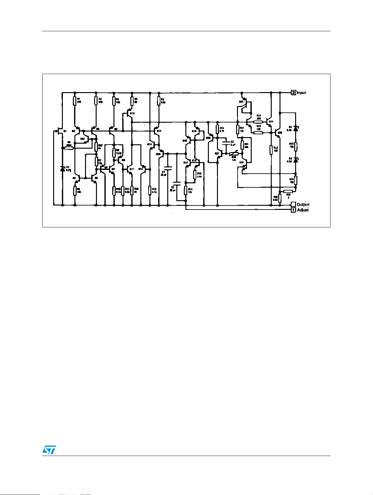
1 Diagram
Figure 1. Schematic diagram
3/23
Pin configuration LM138 - LM238 - LM338
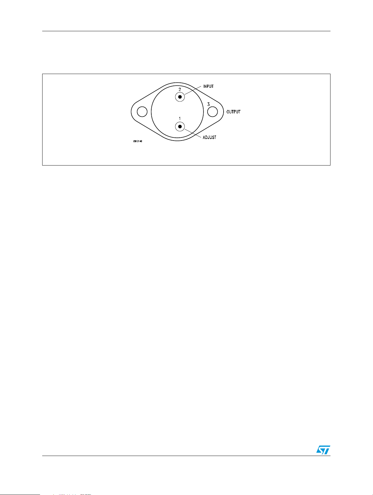
2 Pin configuration
Figure 2. Pin connections (top view)
TO-3
4/23
LM138 - LM238 - LM338 Maximum ratings
3 Maximum ratings
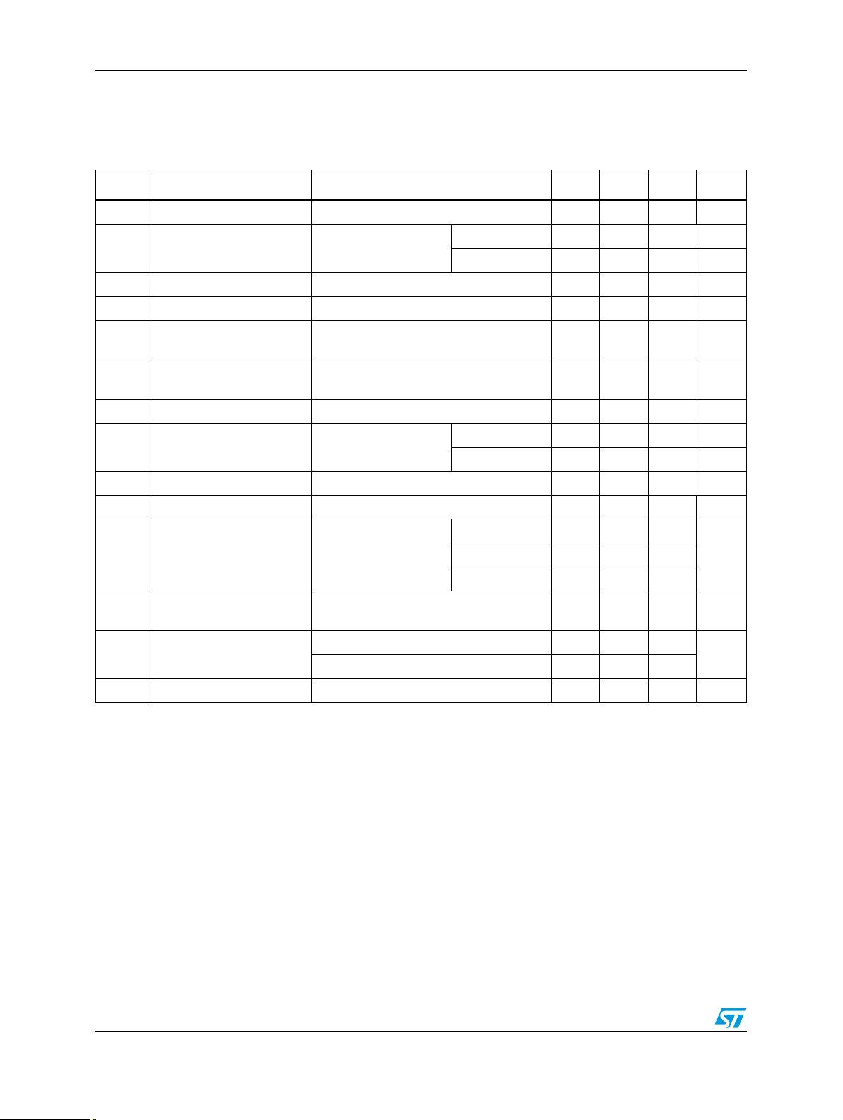
Table 2. Absolute maximum ratings
Symbol Parameter Value Unit
V
- VOInput-output voltage differential 35
I
T
T
P
D
STG
LEAD
Power dissipation Internally limited
Storage temperature range -65 to 150 °C
Lead temperature (Soldering, 10 seconds) 300 °C
LM138 -55 to 150
V
T
OP
Operating junction temperature range
°CLM238 -25 to 125
LM338 0 to 125
Note: Absolute maximum ratings are those values beyond which damage to the device may occur.
Functional operation under these condition is not implied.
Table 3. Thermal data
Symbol Parameter Value Unit
R
R
thJC
thJA
Thermal resistance junction-case 1.4 °C/W
Thermal resistance junction-ambient 35 °C/W
5/23
Electrical characteristics LM138 - LM238 - LM338
4 Electrical characteristics
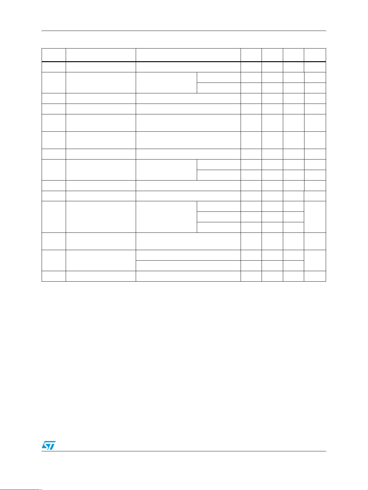
Table 4. Electrical characteristics for LM138/LM238
(1)
Symbol Parameter Test conditions Min. Typ. Max. Unit
K
Line regulation
VI
K
Load regulation
VO
(2)
(2)
TA = 25°C, VI - VO = 3 to 35 V 0.005 0.01 %/V
≤ 5 V 5 15 mV
V
TA = 25°C
= 10 mA to 5 A
I
O
O
V
≥ 5 V 0.1 0.3 %
O
Thermal regulation Pulse = 20 ms 0.002 0.01 %/W
I
ΔI
V
K
K
I
O(MIN)
Adjustment pin current 45 100 µA
ADJ
Adjustment pin current
ADJ
change
Reference voltage
REF
Line regulation
K
VI
Load regulation
VO
Temperature stability TJ = T
VT
(2)
(2)
= 10 mA to 5 A, VI - VO = 3 to 35 V 0.2 5 µA
I
L
- VO = 3 to 35 V, IO = 10 mA to 5 A
V
I
P ≤ 50 W
1.19 1.24 1.29 V
VI - VO = 3 to 35 V 0.02 0.04 %/V
V
≤ 5 V 20 30 mV
IO = 10 mA to 5 A
to T
MIN
MAX
O
V
≥ 5 V 0.3 0.6 %
O
1%
Minimum load current VI - VO ≤ 35 V 3.5 5 mA
DC 5 8
I
O(MAX)
V
R
K
1. (T
2. Regulation is measured at constant junction temperature. Changes in output voltage due to heating effects are taken into
Current limit VI - VO ≤ 10 V
- VO = 30 V 1
V
I
RMS output noise (% of
NO
VO)
Ripple rejection ratio
VF
Long term stability TA = 125°C 0.3 1 %
VH
= -55 to 150 °C for LM138, TJ = -25 to 150 °C for LM238, VI - VO = 5 V, IO = 2.5 A. Although power dissipation is
J
internally limited, these specifications apply to power dissipation up to 50 W, unless otherwise specified)
account separately by thermal rejection.
= 25°C, f = 10 Hz to 10 kHz 0.003 %
T
a
V
= 10 V, f = 120 Hz 60
O
= 10 µF 60 75
C
ADJ
A0.5 ms Peak 7 12
dB
6/23
LM138 - LM238 - LM338 Electrical characteristics
Table 5. Electrical characteristics for LM338
(1)
Symbol Parameter Test conditions Min. Typ. Max. Unit
K
Line regulation
VI
K
Load regulation
VO
(2)
(2)
TA = 25°C, VI - VO = 3 to 35 V 0.005 0.03 %/V
≤ 5 V 5 25 mV
V
TA = 25°C
= 10 mA to 5 A
I
O
O
V
≥ 5 V 0.1 0.5 %
O
Thermal regulation Pulse = 20 ms 0.002 0.02 %/W
I
ΔI
V
K
K
I
O(MIN)
Adjustment pin current 45 100 µA
ADJ
Adjustment pin current
ADJ
change
Reference voltage
REF
Line regulation
K
VI
Load regulation
VO
Temperature stability TJ = T
VT
(2)
(2)
= 10 mA to 5 A, VI - VO = 3 to 35 V 0.2 5 µA
I
L
- VO = 3 to 35 V, IO = 10 mA to 5 A
V
I
P ≤ 50 W
1.19 1.24 1.29 V
VI - VO = 3 to 35 V 0.02 0.06 %/V
V
≤ 5 V 20 50 mV
IO = 10 mA to 5 A
to T
MIN
MAX
O
V
≥ 5 V 0.3 1 %
O
1%
Minimum load current VI - VO ≤ 35 V 3.5 10 mA
DC 5 8
I
O(MAX)
V
R
K
1. (TJ = 0 to150 °C, VI - VO = 5 V, IO = 2.5 A. Although power dissipation is internally limited, these specifications apply to
2. Regulation is measured at constant junction temperature. Changes in output voltage due to heating effects are taken into
Current limit VI - VO ≤ 10 V
- VO = 30 V 1
V
I
RMS output noise (% of
NO
VO)
Ripple rejection ratio
VF
Long term stability TA = 125°C 0.3 1 %
VH
power dissipation up to 50 W, unless otherwise specified)
account separately by thermal rejection.
= 25°C, f = 10 Hz to 10 kHz 0.003 %
T
a
V
= 10 V, f = 120 Hz 60
O
= 10 µF 60 75
C
ADJ
A0.5 ms Peak 7 12
dB
7/23

Typical characteristics LM138 - LM238 - LM338
5 Typical characteristics
Figure 3. Current limit Figure 4. Current limit
Figure 5. Current limit Figure 6. Load regulation
8/23

LM138 - LM238 - LM338 Typical characteristics
Figure 7. Dropout voltage Figure 8. Adjustment current
Figure 9. Temperature stability Figure 10. Output impedance
9/23

Typical characteristics LM138 - LM238 - LM338
Figure 11. Minimum operating current Figure 12. Ripple rejection
Figure 13. Ripple rejection Figure 14. Ripple rejection
10/23

LM138 - LM238 - LM338 Typical characteristics
Figure 15. Line transient response Figure 16. Load transient response
11/23

Typical application LM138 - LM238 - LM338
6 Typical application
Figure 17. 1.2 V to 25 V adjustable regulator
Needed if device is far from filter capacitors.
* Optional-improves transient response. Output capacitors in the range of 1mF to 100mF of aluminium or
tantalum electrolytic are commonly used to provide improved output impedance and rejection of transients
= 1.25 V (1 + R2/R1)
** V
O
= 240 Ω for LM138 and LM238
*** R
1
12/23

LM138 - LM238 - LM338 Application hints
7 Application hints
In operation, the LM338 develops a nominal 1.25 V reference voltage, V
output and adjustment terminal. The reference voltage is impressed across program resistor
R
and, since the voltage is constant, a constant current I1 then flows through the output set
1
resistor R
V
= V
O
, giving an output voltage of
2
(1+ R2/R1) + I
(REF)
Figure 18. Application circuit
ADJR2
, between the
(REF)
Since the 50 µA current from the adjustment terminal represents an error term, the LM338
was designed to minimize I
ADJ
this, all quiescent operating current is returned to the output establishing a minimum load
current requirement. If there is insufficient load on the output, the output will rise.
7.1 External capacitors
An input bypass capacitor is recommended. A 0.1 µF disc or 1 µF solid tantalum on the input
is suitable input by passing for almost all applications. The device is more sensitive to the
absence of input bypassing when adjustment or output capacitors are used by the above
values will eliminate the possibility of problems. The adjustment terminal can be bypassed
to ground on the LM338 to improve ripple rejection. This bypass capacitor prevents ripple
form being amplified as the output voltage is increased. With a 10 µF bypass capacitor 75
dB ripple rejection is obtainable at any output level. Increases over 20 µF do not appreciably
improve the ripple rejection at frequencies above 120 Hz. If the bypass capacitor is used, it
is sometimes necessary to include protection diodes to prevent the capacitor from
discharging through internal low current paths and damaging the device. In general, the best
type of capacitors to use are solid tantalum. Solid tantalum capacitors have low impedance
even at high frequencies. Depending upon capacitor construction, it takes about 25 µF in
aluminum electrolytic to equal 1 µF solid tantalum at high frequencies. Ceramic capacitors
are also good at high frequencies, but some types have a large decrease in capacitance at
frequencies around 0.5 MHz. For this reason, 0.01 µF disc may seem to work better than a
and make it very constant with line and load changes. To do
13/23

Application hints LM138 - LM238 - LM338
0.1 µF disc as a bypass. Although the LM338 is stable with no output capacitors, like any
feedback circuit, certain values of external capacitance can cause excessive ringing. This
occurs with values between 500 pF and 5000 pF. A 1 mF solid tantalum (or 25 µF aluminium
electrolytic) on the output swamps this effect and insures stability.
7.2 Load regulation
The LM338 is capable of providing extremely good load regulation but a few precautions are
needed to obtain maximum performance. The current set resistor connected between the
adjustment terminal and the output terminal (usually 240 Ω) should be tied directly to the
output of the regulator rather than near the load. This eliminates line drops from appearing
effectively in series with the reference and degrading regulation. For example, a 15 V
regulator with 0.05 Ω resistance between the regulator and load will have a load regulation
due to line resistance of 0.05 Ω x I
effective line resistance will be 0.05 Ω (1 + R
on page 8 shows the effect of resistance between the regulator and 140 Ω set resistor. With
the TO-3 package, it is easy to minimize the resistance from the case to the set resistor, by
using 2 separate leads to the case. The ground of R
load to provide remote ground sensing and improve load regulation.
. If the set resistor is connected near the load the
L
) or in this case, 11.5 times worse. Figure 4
2/R1
can be returned near the ground of the
2
7.3 Protection diodes
When external capacitors are used with any IC regulator it is sometimes necessary to add
protection diodes to prevent the capacitors from discharging through low current points into
the regulator. Most 20 µF capacitors have low enough internal series resistance to deliver
20 A spikes when shorted. Although the surge is short, there is enough energy to damage
parts of the IC. When an output capacitor is connected to a regulator and the input is
shorted, the output capacitor will discharge into the output of the regulator. The discharge
current depends on the value of the capacitor, the output voltage of the regulator, and the
rate of decrease of V
able to sustain 25 A surge with no problem. This is not true of other types of positive
regulators. For output capacitors of 100 µF or less at output of 15 V or less, there is no need
to use diodes.The bypass capacitor on the adjustment terminal can discharge through a low
current junction. Discharge occurs when either the input or output is shorted. Internal to the
LM338 is a 50 Ω resistor which limits the peak discharge current. No protection is needed
for output voltages of 25 V or less and 10 µF capacitance. Figure 5 on page 8 shows an
LM338 with protection diodes included for use with outputs greater than 25 V and high
values of output capacitance output capacitance an LM338 with protection diodes included
for use with outputs greater than 25 V and high values of output capacitance.
. In the LM338 this discharge path is through a large junction that is
I
14/23

LM138 - LM238 - LM338 Application hints
Figure 19. Regulator with line resistance in output lead
Figure 20. Regulator with protection diodes
15/23

Application hints LM138 - LM238 - LM338
Figure 21. 10 A regulator
* Minimum load - 100 mA
≥ 10 V
V
I
≥ 3 V
V
O
- VO ≥ 3.5 V
V
I
Figure 22. 5 A current regulator
* Minimum load - 100 mA
≥ 10 V
V
I
≥ 3 V
V
O
16/23

LM138 - LM238 - LM338 Application hints
Figure 23. 15 A regulator
* Minimum load - 100mA
≥ 10 V
V
I
≥ 3 V
V
O
- VO ≥ 4V
V
I
17/23

Application hints LM138 - LM238 - LM338
Figure 24. 5 V logic regulator with electronic shutdown
* R1 = 240 Ω for LM138 or LM238
= 720 Ω for LM138 or LM238
* R
2
** Minimum load - 100 mA
Figure 25. Tracking pre-regulator
= 240 Ω for LM138 or LM238
* R
1
= 720 Ω for LM138 or LM238
* R
2
* * Minimum output = 1.2 V
18/23

LM138 - LM238 - LM338 Application hints
Figure 26. Slow turn-on 15 V regulator
* R1 = 240 Ω for LM138 or LM238
= 2.7 kΩ for LM138 or LM238
* R
2
19/23

Package mechanical data LM138 - LM238 - LM338
8 Package mechanical data
In order to meet environmental requirements, ST offers these devices in ECOPACK®
packages. These packages have a lead-free second level interconnect. The category of
second Level Interconnect is marked on the package and on the inner box label, in
compliance with JEDEC Standard JESD97. The maximum ratings related to soldering
conditions are also marked on the inner box label. ECOPACK is an ST trademark.
ECOPACK specifications are available at: www.st.com.
20/23

LM138 - LM238 - LM338 Package mechanical data
TO-3 mechanical data
Dim.
A 11.85 0.466
B0.96 1.05 1.10 0.037 0.041 0.043
C 1.70 0.066
D 8.7 0.342
E 20.0 0.787
G 10.9 0.429
N 16.9 0.665
P 26.2 1.031
R 3.88 4.09 0.152 0.161
U 39.5 1.555
V 30.10 1.185
Min. Typ. Max. Min. Typ. Max.
mm. inch.
P
A
G
U
V
N
O
B
D
C
E
R
P003C/C
21/23

Revision history LM138 - LM238 - LM338
9 Revision history
Table 6. Document revision history
Date Revision Changes
16-Apr-2003 1 First release.
11-Apr-2008 2 Added: Table 1 on page 1.
22/23

LM138 - LM238 - LM338
Please Read Carefully:
Information in this document is provided solely in connection with ST products. STMicroelectronics NV and its subsidiaries (“ST”) reserve the
right to make changes, corrections, modifications or improvements, to this document, and the products and services described herein at any
time, without notice.
All ST products are sold pursuant to ST’s terms and conditions of sale.
Purchasers are solely responsible for the choice, selection and use of the ST products and services described herein, and ST assumes no
liability whatsoever relating to the choice, selection or use of the ST products and services described herein.
No license, express or implied, by estoppel or otherwise, to any intellectual property rights is granted under this document. If any part of this
document refers to any third party products or services it shall not be deemed a license grant by ST for the use of such third party products
or services, or any intellectual property contained therein or considered as a warranty covering the use in any manner whatsoever of such
third party products or services or any intellectual property contained therein.
UNLESS OTHERWISE SET FORTH IN ST’S TERMS AND CONDITIONS OF SALE ST DISCLAIMS ANY EXPRESS OR IMPLIED
WARRANTY WITH RESPECT TO THE USE AND/OR SALE OF ST PRODUCTS INCLUDING WITHOUT LIMITATION IMPLIED
WARRANTIES OF MERCHANTABILITY, FITNESS FOR A PARTICULAR PURPOSE (AND THEIR EQUIVALENTS UNDER THE LAWS
OF ANY JURISDICTION), OR INFRINGEMENT OF ANY PATENT, COPYRIGHT OR OTHER INTELLECTUAL PROPERTY RIGHT.
UNLESS EXPRESSLY APPROVED IN WRITING BY AN AUTHORIZED ST REPRESENTATIVE, ST PRODUCTS ARE NOT
RECOMMENDED, AUTHORIZED OR WARRANTED FOR USE IN MILITARY, AIR CRAFT, SPACE, LIFE SAVING, OR LIFE SUSTAINING
APPLICATIONS, NOR IN PRODUCTS OR SYSTEMS WHERE FAILURE OR MALFUNCTION MAY RESULT IN PERSONAL INJURY,
DEATH, OR SEVERE PROPERTY OR ENVIRONMENTAL DAMAGE. ST PRODUCTS WHICH ARE NOT SPECIFIED AS "AUTOMOTIVE
GRADE" MAY ONLY BE USED IN AUTOMOTIVE APPLICATIONS AT USER’S OWN RISK.
Resale of ST products with provisions different from the statements and/or technical features set forth in this document shall immediately void
any warranty granted by ST for the ST product or service described herein and shall not create or extend in any manner whatsoever, any
liability of ST.
ST and the ST logo are trademarks or registered trademarks of ST in various countries.
Information in this document supersedes and replaces all information previously supplied.
The ST logo is a registered trademark of STMicroelectronics. All other names are the property of their respective owners.
© 2008 STMicroelectronics - All rights reserved
STMicroelectronics group of companies
Australia - Belgium - Brazil - Canada - China - Czech Republic - Finland - France - Germany - Hong Kong - India - Israel - Italy - Japan -
Malaysia - Malta - Morocco - Singapore - Spain - Sweden - Switzerland - United Kingdom - United States of America
www.st.com
23/23
 Loading...