

Features
LM137
LM337
Three-terminal adjustable negative voltage regulators
■ Output voltage adjustable down to V
■
1.5 A guaranteed output current
■ 0.3%/V typical load regulation
■ 0.01%/V typical line regulation
■ Current limit constant with temperature
■ Ripple rejection: 77 dB
■ Standard 3-lead transistor packages
■ Excellent thermal regulation: 0.002%/V
■ 50 ppm/°C temperature coefficient
REF
Description
The LM137 series are adjustable 3-terminal
negative voltage regulators capable of supplying
in excess -1.5 A over a -1.2 to -37 V output
voltage range. They are exceptionally easy to use
and require only two external resistors to set the
output voltage. Further, both line and load
regulation are better than standard fixed
regulators. Also, LM137 regulators are supplied in
standard transistor packages which are easily
mounted and handled. In addition to higher
performance than fixed regulators, the LM137
series offer full overload protection available only
in integrated circuits. Included on the chip are
current limit, thermal overload protection and safe
area protection. All overload protection circuitry
remains fully functional even if the adjustment
terminal is disconnected.
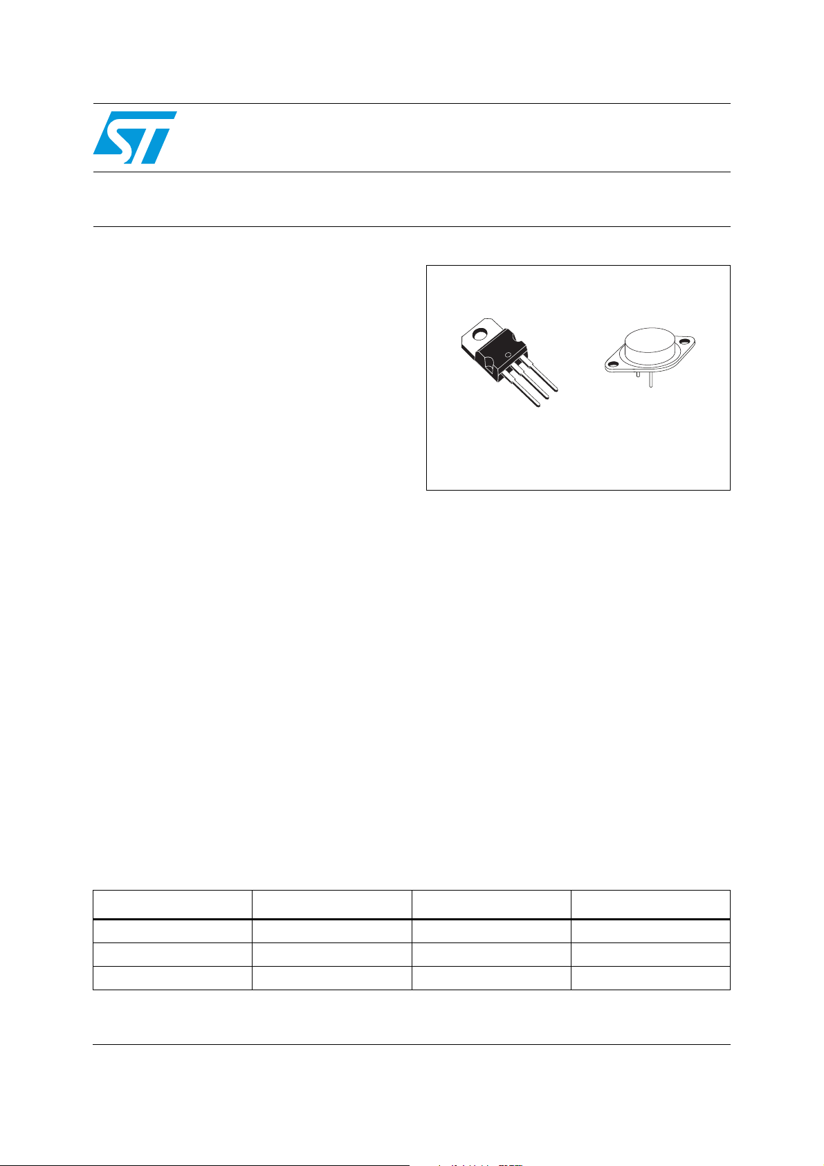
TO-220
TO-3
Table 1. Device summary
Part numbers Order codes Packages Temperature range
LM137 LM137K TO-3 - 55 °C to 150 °C
LM337 LM337K TO-3 0 °C to 125 °C
LM337 LM337SP TO-220 0 °C to 125 °C
October 2011 Doc ID 2167 Rev 4 1/18
www.st.com
18

Contents LM137, LM337
Contents
1 Diagram . . . . . . . . . . . . . . . . . . . . . . . . . . . . . . . . . . . . . . . . . . . . . . . . . . . 3
2 Pin configuration . . . . . . . . . . . . . . . . . . . . . . . . . . . . . . . . . . . . . . . . . . . . 4
3 Maximum ratings . . . . . . . . . . . . . . . . . . . . . . . . . . . . . . . . . . . . . . . . . . . . 5
4 Electrical characteristics . . . . . . . . . . . . . . . . . . . . . . . . . . . . . . . . . . . . . 6
5 Typical characteristics . . . . . . . . . . . . . . . . . . . . . . . . . . . . . . . . . . . . . . . 8
6 Thermal regulation . . . . . . . . . . . . . . . . . . . . . . . . . . . . . . . . . . . . . . . . . 10
7 Typical application . . . . . . . . . . . . . . . . . . . . . . . . . . . . . . . . . . . . . . . . . 11
8 Package mechanical data . . . . . . . . . . . . . . . . . . . . . . . . . . . . . . . . . . . . 14
9 Revision history . . . . . . . . . . . . . . . . . . . . . . . . . . . . . . . . . . . . . . . . . . . 17
2/18 Doc ID 2167 Rev 4
LM137, LM337 Diagram
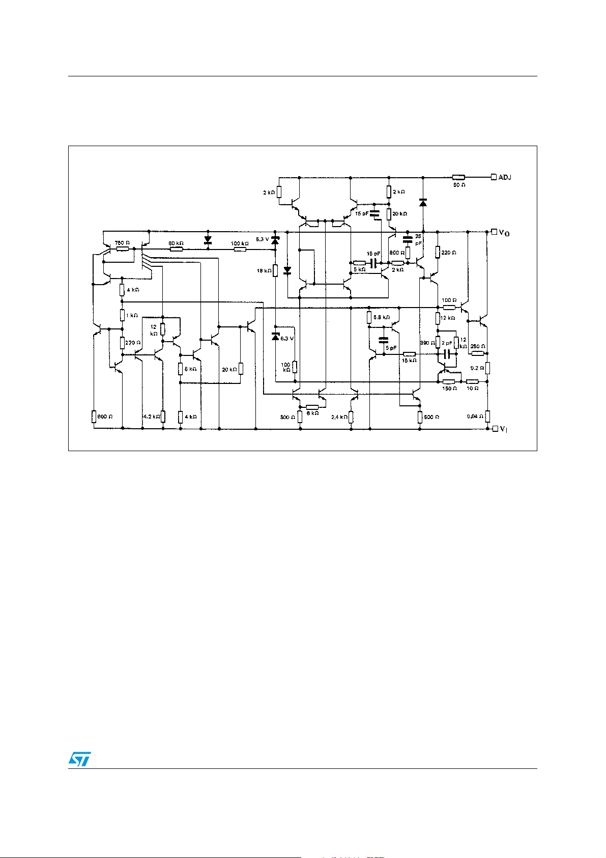
1 Diagram
Figure 1. Schematic diagram
Doc ID 2167 Rev 4 3/18
Pin configuration LM137, LM337
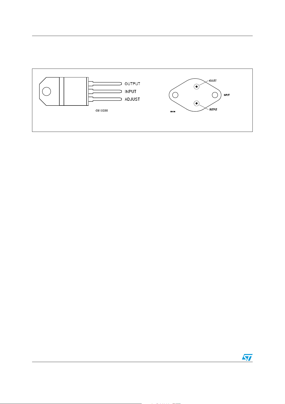
2 Pin configuration
Figure 2. Pin connections (top view)
TO-220
TO-3
4/18 Doc ID 2167 Rev 4
LM137, LM337 Maximum ratings
3 Maximum ratings
Table 2. Absolute maximum ratings
Symbol Parameter Value Unit
- VOInput output voltage differential 40 V
V
I
I
P
T
STG
T
OP
Note: Absolute maximum ratings are those values beyond which damage to the device may occur.
Table 3. Thermal data
Output current 1.5 A
O
Power dissipation Internally limited
D
Storage temperature range - 65 to 150 °C
Operating junction temperature range
LM137 - 55 to 150
LM337 0 to 125
Functional operation under these condition is not implied.
°C
Symbol Parameter TO-220 TO-3 Unit
R
R
thJC
thJA
Thermal resistance junction-case max. 3 4 °C/W
Thermal resistance junction-ambient max. 70 35 °C/W
Doc ID 2167 Rev 4 5/18
Electrical characteristics LM137, LM337
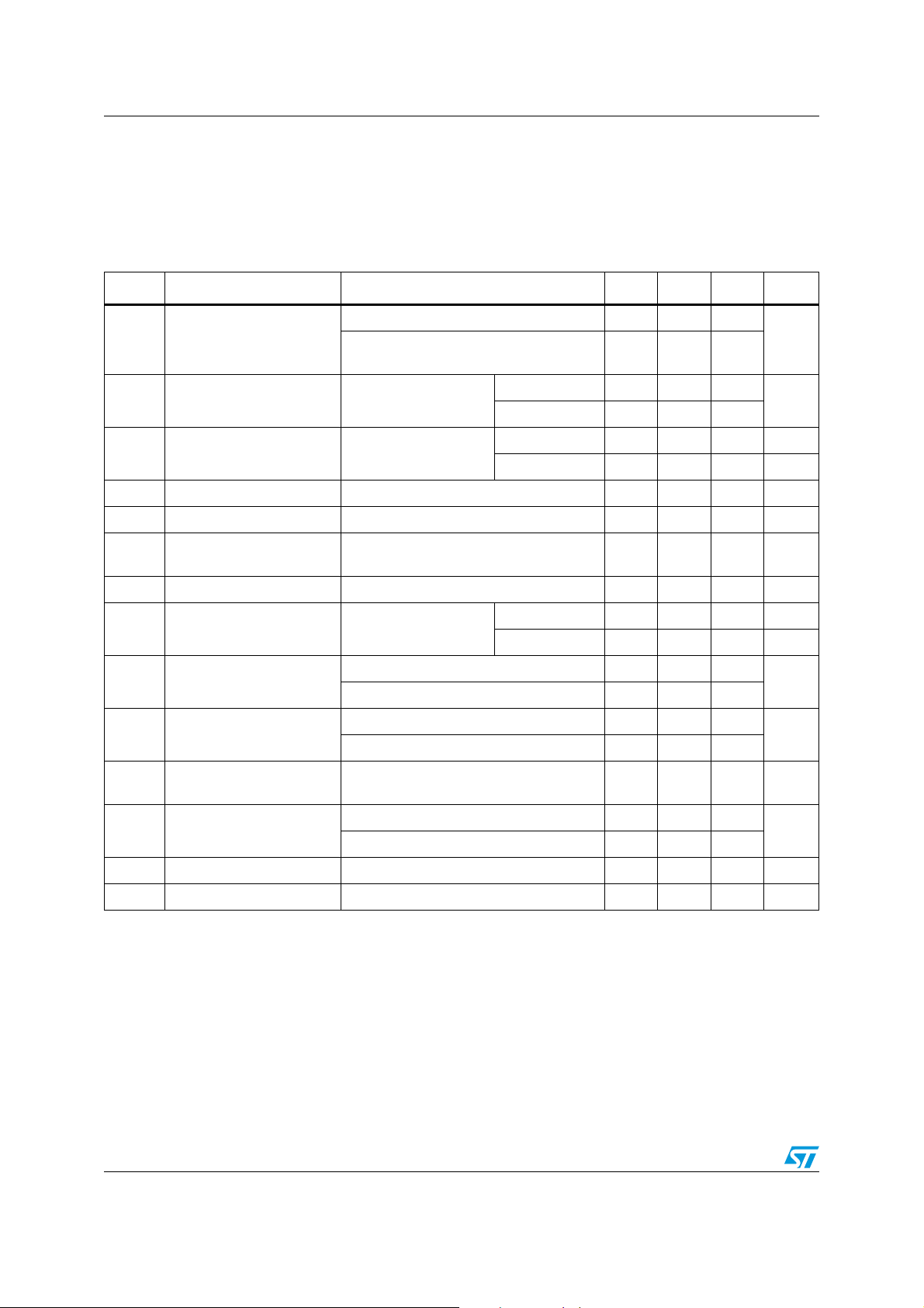
4 Electrical characteristics
TJ = -55 to 150 °C, VI - VO = 5 V, IO = 0.5 A unless otherwise specified.
Table 4. Electrical characteristics of LM137
Symbol Parameter Test conditions Min. Typ. Max. Unit
Ta = 25°C -1.225 -1.25 -1.275
V
K
I
ΔI
K
|I
O(min)
V
R
K
K
1. Regulation is measured at constant junction temperature, using pulse testing with a low duty cycle. Changes in output
Reference voltage
REF
K
VI
VO
Line regulation
Load regulation
(1)
(1)
Thermal regulation T
Adjustment pin current 65 100 µA
ADJ
Adjustment pin current
ADJ
change
K
VI
VO
Line regulation
Load regulation
(1)
(1)
| Minimum load current
I
Short circuit output current
OS
RMS output noise
NO
(% of V
Ripple rejection ratio
VF
Temperature stability 0.6 %
VT
Long term stability Ta = 125°C, 1000 H 0.3 1 %
VH
voltage due to heating effects are covered under the specification for thermal regulation.
)
O
|V
- VO| = 3 to 40 V, TJ = T
I
|IO| = 10mA to |I
O(max)
| P ≤ P
Ta = 25°C
- VO| = 3 to 40 V
|V
I
Ta = 25°C
|IO| = 10mA to |I
= 25°C, pulse 10 ms 0.002 0.02 %/W
a
O(max)
|
Ta = 25°C, |IO| = 10 mA to |I
|VI - VO| = 3 to 40 V
to T
min
max
max
-1.2 -1.25 -1.3
IO = 0.1 A 0.01 0.02
= 20 mA 0.01 0.02
I
O
| ≤ 5 V 15 25 mV
|V
O
| ≥ 5 V 0.3 0.5 %
|V
O
|
O(max)
25µA
|VI - VO| = 3 to 40 V 0.02 0.05 %/V
|VO| ≤ 5 V 20 50 mV
|IO| = 10mA to |I
|V
- VO| ≤ 40 V 2.5 5
I
- VO| ≤ 10 V 1.2 3
|V
I
|V
- VO| ≤ 15 V 1.5 2.2
I
- VO| = 40 V, TJ =25°C 0.24 0.4
|V
I
= 25°C, f = 10 Hz to 10 kHz 0.003 %
T
a
V
= -10 V, f = 120 Hz 60
O
= 10 µF 66 77
C
ADJ
O(max)
|
| ≥ 5 V 0.3 1 %
|V
O
V
%/V
mA
A
dB
= 0 to 150 °C unless otherwise specified.
T
J
6/18 Doc ID 2167 Rev 4

LM137, LM337 Electrical characteristics
Table 5. Electrical characteristics of LM337
Symbol Parameter Test conditions Min. Typ. Max. Unit
Ta = 25°C -1.213 -1.25 -1.287
V
K
I
ΔI
K
|I
O(min)
V
R
K
K
1. Regulation is measured at constant junction temperature, using pulse testing with a low duty cycle. Changes in output
Reference voltage
REF
K
VI
VO
Line regulation
Load regulation
(1)
(1)
Thermal regulation T
Adjustment pin current 65 100 µA
ADJ
Adjustment pin current
ADJ
change
K
VI
VO
Line regulation
Load regulation
(1)
(1)
| Minimum load current
I
Short circuit output current
OS
RMS output noise
NO
(% of VO)
Ripple rejection ratio
VF
Temperature stability 0.6 %
VT
Long term stability Ta = 125°C, 1000 H 0.3 1 %
VH
voltage due to heating effects are covered under the specification for thermal regulation.
|V
- VO| = 3 to 40 V, TJ = T
I
|IO| = 10mA to |I
O(max)
|, P ≤ P
Ta = 25°C
- VO| = 3 to 40 V
|V
I
Ta = 25°C
|IO| = 10mA to |I
= 25°C, pulse 10 ms 0.003 0.04 %/W
a
O(max)
|
Ta = 25°C, |IO| = 10 mA to |I
- VO| = 3 to 40 V
|V
I
to T
min
max
max
-1.2 -1.25 -1.3
IO = 0.1 A 0.01 0.04
= 20 mA 0.01 0.04
I
O
| ≤ 5 V 15 50 mV
|V
O
| ≥ 5 V 0.3 1 %
|V
O
|
O(max)
25µA
|VI - VO| = 3 to 40 V 0.02 0.07 %/V
|VO| ≤ 5 V 20 70 mV
|IO| = 10mA to |I
|V
- VO| ≤ 40 V 2.5 10
I
- VO| ≤ 10 V 1.5 6
|V
I
|V
- VO| ≤ 15 V 1.5 2.2
I
- VO| = 40 V, TJ =2 5°C 0.15 0.4
|V
I
= 25°C, f = 10 Hz to 10 kHz 0.003 %
T
a
V
= -10 V, f = 120 Hz 60
O
= 10 µF 66 77
C
ADJ
O(max)
|
| ≥ 5 V 0.3 1.5 %
|V
O
V
%/V
mA
A
dB
Doc ID 2167 Rev 4 7/18

Typical characteristics LM137, LM337
5 Typical characteristics
Figure 3. Load regulation Figure 4. Current limit
Figure 5. Adjustment current Figure 6. Dropout voltage
Figure 7. Temperature stability Figure 8. Minimum operating current
8/18 Doc ID 2167 Rev 4

LM137, LM337 Typical characteristics
Figure 9. Ripple rejection vs. output voltage Figure 10. Ripple rejection vs. frequency
Figure 11. Ripple rejection vs. output current Figure 12. Output impedance
Figure 13. Line transient response Figure 14. Load transient response
Doc ID 2167 Rev 4 9/18

Thermal regulation LM137, LM337
6 Thermal regulation
When power is dissipated in an IC, a temperature gradient occurs across the IC chip
affecting the individual IC circuit components. With an IC regulator, this gradient can be
especially severe since power dissipation is large.
Thermal regulation is the effect of these temperature gradients on output voltage (in
percentage output change) per watt of power change in a specified time. Thermal regulation
error is independent of electrical regulation or temperature coefficient, and occurs within 5
ms to 50 ms after a change in power dissipation. Thermal regulation depends on IC layout
as well as electrical design. The thermal regulation of a voltage regulator is defined as the
percentage change of V
The LM137 specification is 0.02%/W max. In Figure 1, a typical LM337’s output drifts only 3
mV for 0.03% of V
thus well inside the specification limit of 0.02%/W x 10 W = 0.2% max. When the 10 W pulse
is ended the thermal regulation again shows a 3 mV step as the LM137 chip cools off. Note
that the load regulation error of about 8 mV (0.08%) is additional to the thermal regulation
error.
In Figure 2, when the 10 W pulse is applied for 100 ms, the output drifts only slightly beyond
the drift in the first 10 ms and the thermal error stays well within 0.1% (10 mV).
O
, per watt, within the first 10ms after a step of power, is applied.
O
= – 10 V) when a 10 W pulse is applied for 10 ms. This performance is
10/18 Doc ID 2167 Rev 4

LM137, LM337 Typical application
7 Typical application
Figure 15. Adjustable negative voltage regulator
* C1 = 1 µF solid tantalum or 10 µF aluminium electrolytic required for stability.
** C2 = 1 µF solid tantalum is required only if regulator is more than 10 cm from power supply filter capacitors
Figure 16. Adjustable lab voltage regulator
* The 10 µF capacitors are optimal to improve ripple rejection.
Doc ID 2167 Rev 4 11/18

Typical application LM137, LM337
Figure 17. Current regulator
Figure 18. Negative regulator with protection diodes
* When CL is larger than 20 µF, D1 protects the LM137 in case the input supply is shorted.
** When C2 is larger than 10 µF and V
shorted.
is larger than - 25 V, D2 protects the LM137 in case the output is
O
12/18 Doc ID 2167 Rev 4

LM137, LM337 Typical application
Figure 19. - 5.2 V regulator with electronic shutdown
1. Minimum output = - 1.3 V when control input is low.
Figure 20. Current regulator
(1)
Doc ID 2167 Rev 4 13/18

Package mechanical data LM137, LM337
8 Package mechanical data
In order to meet environmental requirements, ST offers these devices in different grades of
ECOPACK
specifications, grade definitions and product status are available at: www.st.com.
ECOPACK
®
packages, depending on their level of environmental compliance. ECOPACK®
®
is an ST trademark.
14/18 Doc ID 2167 Rev 4

LM137, LM337 Package mechanical data
TO-220 mechanical data
Dim.
A 4.40 4.60 0.173 0.181
C1.23 1.32 0.048 0.051
D 2.40 2.72 0.094 0.107
D1 1.27 0.050
E0.49 0.70 0.019 0.027
F 0.61 0.88 0.024 0.034
F1 1.14 1.70 0.044 0.067
F2 1.14 1.70 0.044 0.067
G4.95 5.15 0.194 0.203
G1 2.4 2.7 0.094 0.106
H2 10.0 10.40 0.393 0.409
L2 16.4 0.645
L4 13.0 14.0 0.511 0.551
L5 2.65 2.95 0.104 0.116
L6 15.25 15.75 0.600 0.620
L7 6.2 6.6 0.244 0.260
L93.5 3.93 0.13 7 0.154
DIA. 3.75 3.85 0.147 0.151
Min. Typ. Max. Min. Typ. Max.
mm. inch.
P011C
Doc ID 2167 Rev 4 15/18

Package mechanical data LM137, LM337
TO-3 mechanical data
Dim.
A 11.85 0.466
B0.96 1.05 1.10 0.037 0.041 0.043
C 1.70 0.066
D 8.7 0.342
E 20.0 0.787
G 10.9 0.429
N 16.9 0.665
P 26.2 1.031
R 3.88 4.09 0.152 0.161
U 39.5 1.555
V 30.10 1.185
Min. Typ. Max. Min. Typ. Max.
mm. inch.
P
A
G
U
V
N
O
B
D
C
E
R
P003C/C
16/18 Doc ID 2167 Rev 4

LM137, LM337 Revision history
9 Revision history
Table 6. Document revision history
Date Revision Changes
19-Jul-2004 1 First issue.
10-Jan-2005 2 Modified pin connection for TO-3.
17-Jul-2008 3 Added: Table 1 on page 1.
03-Oct-2011 4 Modified: Table 1 on page 1.
Doc ID 2167 Rev 4 17/18

LM137, LM337
Please Read Carefully:
Information in this document is provided solely in connection with ST products. STMicroelectronics NV and its subsidiaries (“ST”) reserve the
right to make changes, corrections, modifications or improvements, to this document, and the products and services described herein at any
time, without notice.
All ST products are sold pursuant to ST’s terms and conditions of sale.
Purchasers are solely responsible for the choice, selection and use of the ST products and services described herein, and ST assumes no
liability whatsoever relating to the choice, selection or use of the ST products and services described herein.
No license, express or implied, by estoppel or otherwise, to any intellectual property rights is granted under this document. If any part of this
document refers to any third party products or services it shall not be deemed a license grant by ST for the use of such third party products
or services, or any intellectual property contained therein or considered as a warranty covering the use in any manner whatsoever of such
third party products or services or any intellectual property contained therein.
UNLESS OTHERWISE SET FORTH IN ST’S TERMS AND CONDITIONS OF SALE ST DISCLAIMS ANY EXPRESS OR IMPLIED
WARRANTY WITH RESPECT TO THE USE AND/OR SALE OF ST PRODUCTS INCLUDING WITHOUT LIMITATION IMPLIED
WARRANTIES OF MERCHANTABILITY, FITNESS FOR A PARTICULAR PURPOSE (AND THEIR EQUIVALENTS UNDER THE LAWS
OF ANY JURISDICTION), OR INFRINGEMENT OF ANY PATENT, COPYRIGHT OR OTHER INTELLECTUAL PROPERTY RIGHT.
UNLESS EXPRESSLY APPROVED IN WRITING BY TWO AUTHORIZED ST REPRESENTATIVES, ST PRODUCTS ARE NOT
RECOMMENDED, AUTHORIZED OR WARRANTED FOR USE IN MILITARY, AIR CRAFT, SPACE, LIFE SAVING, OR LIFE SUSTAINING
APPLICATIONS, NOR IN PRODUCTS OR SYSTEMS WHERE FAILURE OR MALFUNCTION MAY RESULT IN PERSONAL INJURY,
DEATH, OR SEVERE PROPERTY OR ENVIRONMENTAL DAMAGE. ST PRODUCTS WHICH ARE NOT SPECIFIED AS "AUTOMOTIVE
GRADE" MAY ONLY BE USED IN AUTOMOTIVE APPLICATIONS AT USER’S OWN RISK.
Resale of ST products with provisions different from the statements and/or technical features set forth in this document shall immediately void
any warranty granted by ST for the ST product or service described herein and shall not create or extend in any manner whatsoever, any
liability of ST.
ST and the ST logo are trademarks or registered trademarks of ST in various countries.
Information in this document supersedes and replaces all information previously supplied.
The ST logo is a registered trademark of STMicroelectronics. All other names are the property of their respective owners.
© 2011 STMicroelectronics - All rights reserved
STMicroelectronics group of companies
Australia - Belgium - Brazil - Canada - China - Czech Republic - Finland - France - Germany - Hong Kong - India - Israel - Italy - Japan -
Malaysia - Malta - Morocco - Philippines - Singapore - Spain - Sweden - Switzerland - United Kingdom - United States of America
www.st.com
18/18 Doc ID 2167 Rev 4
 Loading...